

OXFORD OX16PCI952-TQFP-A Datasheet

Oxford Semiconductor Ltd.
Oxford Semiconductor 2001
A
OX16PCI952 DATA SHEET
Integrated High Performance Dual UARTs,
FEATURES
• Two 16C950 High performance UART channels
• IEEE1284 Compliant SPP/EPP/ECP parallel port
• Multi- function target PCI controller. Fully compliant to
PCI bus specification 2.2 and PCI Power Management
1.0.
• Function access to pre-configure each UART and the
parallel port, prior to handover to generic device
drivers.
• UARTs fully software compatible with 16C550- type
devices.
• Baud rates up to 15Mbps in asynchronous mode and
60Mbps in external 1x clock mode
• 128-byte deep FIFO per transmitter and receiv er
• Flexible clock prescaler from 1 to 31.875
• Automated in-band flow control using programmable
Xon/Xoff in both directions
DESCRIPTION
Parallel Port and 5.0v PCI interface
DS_B008A_00
• Automated out-of-band flow control using CTS#/RTS#
and/or DSR#/DTR#
• Arbitrary trigger levels for receiver and transmitter
FIFO interrupts and automatic in-band and out-ofband flow control
• Infra-red (IrDA) receiver and transmitter operation
• 5, 6, 7, 8 and 9-bits data framing
• Global Interrupt Status and readable FIFO levels to
facilitate implementation of efficient device drivers
• Detection of bad data in the receiver FIFO
• 2 multi-purpose IO pins which can be configured as
interrupt inputs or ‘wake-up’ pins (via local registers).
• Auto-detection of a range of optional MicrowireTM
compatible EEPROMs, to reconfigure device.
• Operation via IO or memory mapping.
• 5.0V operation
• 128 pin TQFP package
The OX16PCI952 is a single chip solution for PCI-based
serial and parallel expansion add-in cards. It is a dual
function device, offering IO or memory mapped access to
the two ultra-high performance OX16C950 UARTs and the
bi-directional parallel port. These functions are defined by
Function 0 and Function 1, respectively. Serial port cards
with 2 serial ports and a parallel port can be designed
without redefining any device parameters.
Each UART channel in the OX16PCI952, is the fastest
available PC-compatible UART, offering data rates up to
15Mbps and 128-byte deep transmitter and receiver FIFOs.
The deep FIFOs reduce CPU overhead and allow
utilisation of higher data rates. Each UART channel is
software compatible with the widely used industry-standard
16C550 devices and compatibles, as well as the
OX16C95x family of high performance UARTs. In addition
to increased performance and FIFO size, the UARTs also
provide the full set of OX16C95x enhanced features
including automated in-band flow control, readable FIFO
levels, etc.
The parallel port is an IEEE 1284 compliant SPP, EPP and
ECP parallel port that fully supports the existing Centronics
interface. For legacy applications, the PCI resources have
been arranged so that the parallel port can be located at
standard I/O addresses
A set of local registers is available to enhance device driver
efficiency and reduce interrupt latency. Each internal UART
has features such as shadowed FIFO fill levels, an interrupt
source register and Good-Data Status, readable in
consecutive DWORD registers and is visible to logical
function0 in both IO space and memory space. The local
registers also provide additional controls for each UART
and the parallel port, to customise the device for the endusers application.
The efficient 32-bit, 33MHz target-only interface is
compliant with the PCI bus specification version 2.2 and
version 1.0 of PCI Power Management Specification.
For full flexibility, all the default configuration register
values can be overwritten using an optional MicrowireTM
compatible serial EEPROM.
This EEPROM can also be used to provide function access
to pre-configure each UART into enhanced modes or preconfigure the parallel port, prior to any PCI configuration
accesses and before control is handed to generic device
drivers.
MicrowireTM is a trade mark of National Semiconductor.
25 Milton Park, Abingdon, Oxon, OX14 4SH, UK
Tel: +44 (0)1235 824900 Fax: +44(0)1235 821141
OX16PCI952 Datasheet rev 1.1 – June 2001
Part No. OX16PCI952-TQFP-

OXFORD SEMICONDUCTOR LTD.
OX16PCI952
CONTENTS
1 PERFORMANCE COMPARISON..................................................................................................4
1.1 IMPROVEMENTS OF THE OX16PCI952 OVER DISCRETE SOLUTIONS:.......................................................................4
2 BLOCK DIAGRAM.......................................................................................................................6
3 PIN INFORMATION .....................................................................................................................7
4 PIN DESCRIPTION......................................................................................................................8
5 CONFIGURATION & OPERATION............................................................................................. 13
6 PCI TARGET CONTROLLER ..................................................................................................... 14
6.1 OPERATION........................................................................................................................................................................14
6.2 CONFIGURATION SPACE.................................................................................................................................................15
6.3 ACCESSING FUNCTION 0 AND FUNCTION 1.................................................................................................................17
6.4 ACCESSING THE LOCAL CONFIGURATION REGISTERS............................................................................................19
6.5 PCI INTERRUPTS...............................................................................................................................................................24
6.6 POWER MANAGEMENT....................................................................................................................................................25
7 INTERNAL OX16C950 UART..................................................................................................... 28
7.1 OPERATION – MODE SELECTION...................................................................................................................................28
7.2 REGISTER DESCRIPTION TABLES .................................................................................................................................30
7.3 RESET CONFIGURATION .................................................................................................................................................34
7.4 TRANSMITTER AND RECEIVER FIFOS...........................................................................................................................35
7.5 LINE CONTROL & STATUS...............................................................................................................................................36
7.6 INTERRUPTS & SLEEP MODE .........................................................................................................................................38
7.7 MODEM INTERFACE.........................................................................................................................................................40
7.8 OTHER STANDARD REGISTERS.....................................................................................................................................41
7.9 AUTOMATIC FLOW CONTROL.........................................................................................................................................42
7.10 BAUD RATE GENERATION ...............................................................................................................................................44
7.11 ADDITIONAL FEATURES ..................................................................................................................................................46
8 BI-DIRECTIONAL PARALLEL PORT ..........................................................................................52
8.1 OPERATION AND MODE SELECTION.............................................................................................................................52
8.2 PARALLEL PORT INTERRUPT.........................................................................................................................................53
8.3 REGISTER DESCRIPTION.................................................................................................................................................54
9 SERIAL EEPROM SPECIFICATION ........................................................................................... 57
9.1 EEPROM DATA ORGANISATION.....................................................................................................................................57
10 OPERATING CONDITIONS..................................................................................................... 61
11 DC ELECTRICAL CHARACTERISTICS................................................................................... 62
11.1 5V STANDARD (NON-PCI) I/O BUFFERS.......................................................................................................................62
11.2 PCI I/O BUFFERS...............................................................................................................................................................62
12 AC ELECTRICAL CHARACTERISTICS................................................................................... 63
12.1 PCI I/O BUFFERS..............................................................................................................................................................63
12.2 SERIAL PORTS ..................................................................................................................................................................63
13 TIMING WAVEFORMS............................................................................................................ 64
14 PACKAGE INFORMATION..................................................................................................... 74
15 ORDERING INFORMATION.................................................................................................... 75
16 CONTACT DETAILS............................................................................................................... 76
DataSheet Revision 1.1 Page 2

OXFORD SEMICONDUCTOR LTD.
This page is intentionally left blank
OX16PCI952
DataSheet Revision 1.1 Page 3

OXFORD SEMICONDUCTOR LTD.
1 PERFORMANCE COMPARISON
Feature OX16PCI952 16C552 + PCI
Internal serial channels 2 0 0
Integral 1284 Compliant parallel port yes no no
Multi- function PCI device yes no no
Support for PCI Power Management yes no no
Zero wait-state read/write operation yes no no
No. of available external interrupt pins 2 2 2
DWORD access to UART Interrupt Source
Registers & FIFO Levels
Good-Data status yes no no
Full Plug and Play with external EEPROM yes yes yes
External 1x baud rate clock yes no no
Max baud rate in normal mode 15 Mbps 115 Kbps 1.5 Mbps
Max baud rate in 1x clock mode 60 Mbps n/a n/a
FIFO depth 128 16 64
Sleep mode yes no yes
Auto Xon/Xoff flow yes no yes
Auto CTS#/RTS# flow yes no yes
Auto DSR#/DTR# flow yes no no
No. of Rx interrupt thresholds 128 4 4
No. of Tx interrupt thresholds 128 1 4
No. of flow control thresholds 128 n/a 4
Transmitter empty interrupt yes no no
Readable status of flow control yes no no
Readable FIFO levels yes no no
Clock prescaler options 248 n/a 2
Rx/Tx disable yes no no
Software reset yes no no
Device ID yes no no
9-bit data frames yes no no
RS485 buffer enable yes no no
Infra-red (IrDA) yes no yes
16C652 + PCI
Bridge
yes no no
Bridge
OX16PCI952
Table 1: OX16PCI952 performance compared with PCI Bridge + generic UART/Parallel Port Combinations.
1.1 Improvements of the OX16PCI952 over discrete solutions:
Higher degree of integration:
The OX16PCI952 offers two internal ultra-high
performance 16C950 UARTs and one IEEE1284 compliant
bi-directional parallel port.
UART device driver efficiency is increased by using each
channel’s features such as the 128-byte deep transmitter &
receiver FIFOs, flexible clock options, automatic flow
control, programmable interrupt and flow control trigger
levels and readable FIFO levels. Data rates of each UART
is up to 60Mbps.
DataSheet Revision 1.1 Page 4
Improved access timing:
Access to the internal UARTs require zero or one PCI wait
states. A PCI read transaction from an internal UART can
complete within five PCI clock cycles and a write
transaction to an internal UART can complete within four
PCI clock cycles.
Reduces interrupt latency:
The OX16PCI952 offers shadowed FIFO levels and
Interrupt status registers of the internal UARTs, as well as
general device interrupt status, to reduce the device driver
interrupt latency.

OXFORD SEMICONDUCTOR LTD.
Power management:
Both functions of the OX16PCI952 comply with the PCI
Power Management Specification 1.0 and the PC98/99
Power Management specifications, by offering the
extended capabilities for Power Management and
supporting the power states D0, D2 and D3. This achieves
significant power savings by allowing device drivers to
power down the PCI functions and disable the UART
channels and the parallel port.
A ‘wake-up’ event (the ‘power management event’) is
requested via the PME# pin from either of the power states
D2 or D3. For the UART channels, this wake-up request is
generated through the UART line RI (for power state D3),
and any modem line and the Serial Data In (for power state
D2). For the parallel port, this wake-up request is
generated through the multi-purpose IO pins, MIO(1:0).
OX16PCI952
Optional EEPROM:
The OX16PCI952 can be reconfigured from an external
Microwire
in many applications as default values are provided for
typical applications. Features available via the use of the
EEPROM include redefining device ID’s and vendor/subvendor ID fields in the PCI header space, selectively
enabling/disabling interrupts, powerdown and wakeup
requests, and performing function access to pre-configure
the UARTs and the parallel port.
Multi-function device:
The OX16PCI952 is a multi -function device to enable users
to load individual device drivers for the internal serial ports
and the internal parallel port.
TM
based EEPROM. However, this is not required
DataSheet Revision 1.1 Page 5
OXFORD SEMICONDUCTOR LTD.
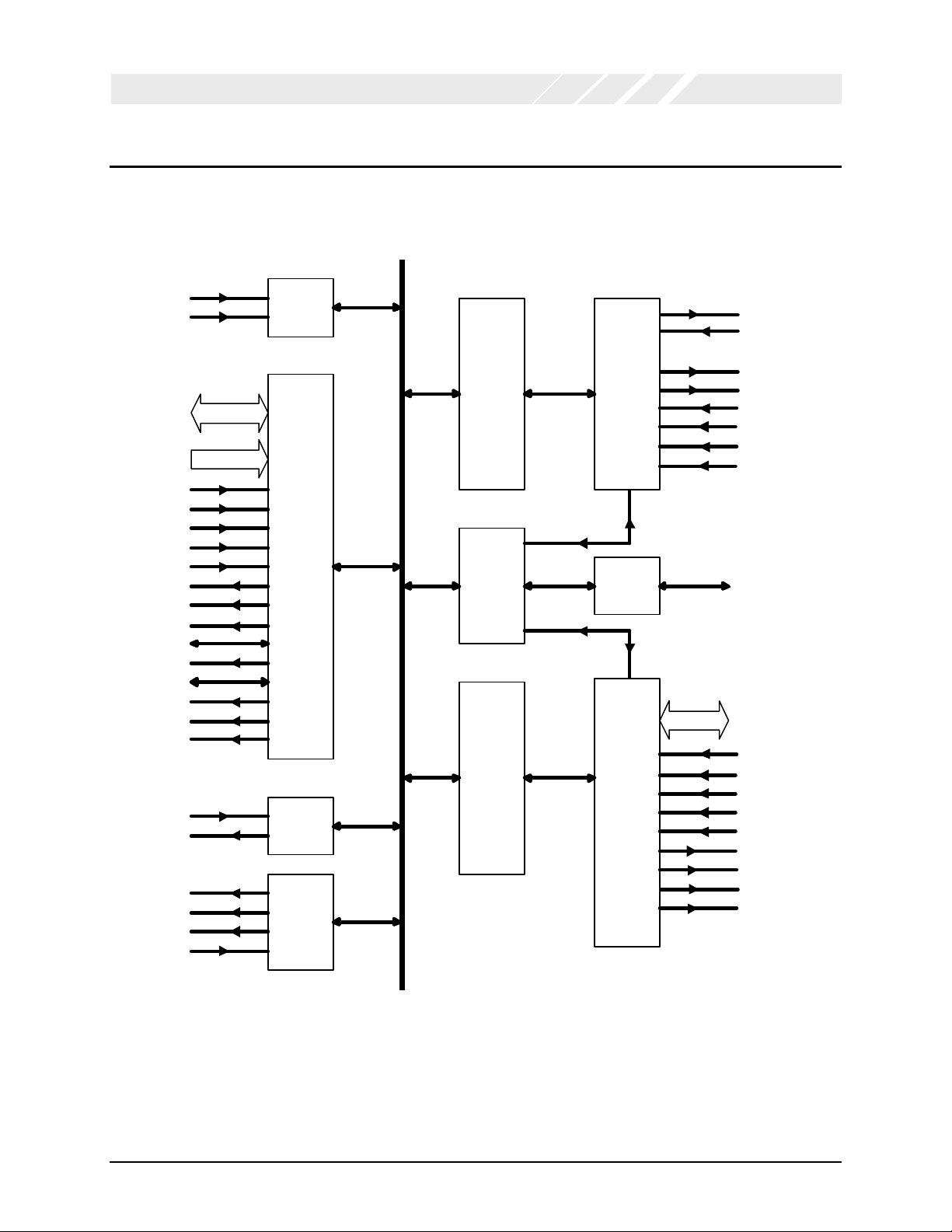
2 BLOCK DIAGRAM
OX16PCI952
Mode0
Fifosel
AD[31:0]
C/BE[3:0]
PCI Clk
RST#
IDSEL
FRAME#
IRDY#
TRDY#
STOP#
DEVSEL#
PAR
SERR#
PERR#
INTA#
INTB#
PME#
XTLI
XTLO
EE_DO
EE_CK
EE_CS
EE_DI
Config
Interface
PCI
Interface
Clock &
Baud Rate
Generator
EEPROM
Interface
Function 0
Interrupt
Logic
Function 1
Dual
UARTs
MIO logic
Parallel
Port
SOUT[1:0]
SIN[1:0]
RTS[1:0]
DTR[1:0]
CTS[1:0]
DSR[1:0]
DCD[1:0]
RI[1:0]
MIO[1:0]
PD[7:0]
ACK#
PE
BUSY
SLCT
ERR#
SLIN#
INIT#
AFD#
STB#
Internal Data/Control Bus
Figure 1: OX16PCI952 Block Diagram
DataSheet Revision 1.1 Page 6

OXFORD SEMICONDUCTOR LTD.
3 PIN INFORMATION
Package : 128 TQFP. (14mm x 14mm)
OX16PCI952
Z_DSR[1]
Z_CTS[1]
Z_DTR[1]
Z_RTS[1]
EXT_DATA_OUT[1]
GND
VDD
EXT_DATA_IN[0]
Z_RI[0]
Z_DCD[0]
Z_DSR[0]
Z_CTS[0]
Z_DTR[0]
Z_RTS[0]
EXT_DATA_OUT[0]
GND
Z_INTA
Z_INTB
Z_RESET
GND
PCI_CLK
VDD
GND
Z_PME
AD31
AD30
AD29
AD28
AD27
AD26
AD25
GND
Z_DCD[1]
96
97
100
110
EXT_DATA_IN[1]
Z_RI[1]
GND
GND
XTLI
XTLO
VDD
ACK
FIFOSEL
PE
BUSY
ERROR_N
SELCT
GND
INIT_N
SLIN_N
STB_N
AFD_N
VDD
PARALLEL DATA 1
PARALLEL DATA 0
GND
PARALLEL DATA 4
PARALLEL DATA 6
PARALLEL DATA 5
PARALLEL DATA 3
PARALLEL DATA 2
708090
PARALLEL DATA 7
OX16PCI952
120
128
1 32
VDD
AD24
IDSEL
Z_CBE3
AD23
AD22
10 20 30
GND
AD21
AD20
VDD
GND
AD19
AD18
AD17
AD16
Z_CBE2
Z_FRAME
Z_IRDY
GND
GND
VDD
GND
Z_TRDY
Z_DEVSEL
Z_STOP
Z_PERR
PAR
Z_SERR
GND
SEEPROM_SK
LOCAL_TRANS_EN
GND
65
SEEPROM_CS
64
SEEPROM_DO
SEEPROM_DI
GND
MULTI IO 1
60
MULTI IO 0
VDD
GND
MODE0
TEST
GND
GND
AD0
AD1
AD2
50
AD3
AD4
AD5
VDD
GND
AD6
AD7
Z_CBE0
AD8
AD9
40
AD10
VDD
GND
AD11
AD12
AD13
AD14
33
VDD
AD15
Z_CBE1
DataSheet Revision 1.1 Page 7

OXFORD SEMICONDUCTOR LTD.
4 PIN DESCRIPTION
Please refer to Section “Pin Information” for actual Signal Name to Pin Number assignments.
Pins Dir1 Name Description
PCI interface
2, 5, 6, 7, 8, 12, 13, 14, 15,
32, 33, 34, 35, 36, 39, 40, 41,
43, 44, 47, 48, 49, 50, 51, 52,
121, 122, 123, 124, 125, 126,
127
3, 16, 31, 42 P_I C/BE[3:0]# PCI Command/Byte enable
117 P_I PCI CLK PCI system clock
17 P_I FRAME# Cycle Frame
24 P_O DEVSEL# Device Select
18 P_I IRDY# Initiator ready
23 P_O TRDY# Target ready
25 P_O STOP# Target Stop request
28 P_I/O PAR Parity
27 P_O SERR# System error
26 P_I/O PERR# Parity error
4 P_I IDSEL Initialization device select
115 P_I RST# PCI system reset
113
114
120 P_OD PME# Power management event
Serial port pins
88 I FIFOSEL FIFO select.
111
101
111
101
104
94
104
94
P_I/O AD[31:0] Multiplexed PCI Address/Data bus
P_OD INTA#,
INTB#
O
EXT_DATA_OUT[0]
O
EXT_DATA_OUT[1]
O
IrDA_Out[0]
O
IrDA_Out[1]
I
EXT_DATA_IN[0]
I
EXT_DATA_IN[1]
I
IrDA_In[0]
I
IrDA_In[1]
PCI interrupts
For backward compatibility with 16C550, 16C650 and
16C750 devices the FIFO depth of both UARTs is 16 when
FIFOSEL is low. The FIFO size of both UARTs is increased
to 128 when FIFOSEL is high.
The FIFO size of each UART may also be set to 128 by
setting the UARTs FCR[5] when LCR[7] is set, or by putting
the device into enhanced mode.
The unlatched state of this pin is readable by software.
Serial data output, Uart 0
Serial data output, Uart 1.
UART IrDA data outputs, for UART 0 and 1.
Serial data output pins redefined as IrDA data outputs when
MCR[6] of the corresponding UART channel is set in
enhanced mode
Serial data input, UART 0.
Serial data input, UART 1.
UART IrDA data inputs, for UART 0 and 1.
Serial data input pins redefined as IrDA data inputs when
MCR[6] of the corresponding UART channel is set in
enhanced mode
OX16PCI952
DataSheet Revision 1.1 Page 8

OXFORD SEMICONDUCTOR LTD.
Pins Dir1 Name Description
Serial port pins (Contd)
106
96
109
99
109
99
109
99
110
100
108
98
107
97
107
97
105
95
105
95
O
O
O
O
O
O
O
O
I
I
I
I
I
I
I
I
I
I
I
I
DCD[0]#
DCD[1]#
DTR[0]#
DTR[1]#
485_En[0]
485_En[1]
Tx_Clk_Out[0]
Tx_Clk_Out[1]
RTS[0]#
RTS[1]#
CTS[0]#
CTS[1]#
DSR[0]#
DSR[1]#
Rx_Clk_In[0]
Rx_Clk_In[0]
RI[0]#
RI[1]#
Tx_Clk_In[0]
Tx_Clk_In[0]
OX16PCI952
Active-low modem “data-carrier-detect” input, for UART 0
and UART 1.
Active-low modem “data -terminal-ready output”, for UART 0
and UART 1.
If automated DTR# flow control is enabled for the
corresponding UART channel, the DTR# pin is asserted and
deasserted if the receiver FIFO reaches or falls below the
channel’s programmed thresholds, respectively.
In RS485 half-duplex mode, the DTR# pin of each UART
channel may be programmed to reflect the state of the
channel’s transmitter empty bit to automatically control the
direction of the RS485 transceiver buffer (see register
ACR[4:3])
Transmitter 1x clock (baud rate generator output).
For isochronous applications, the 1x (or Nx) transmitter clock
of each UART channel may be asserted on the DTR# pins
(see register CKS[5:4])
Active-low modem “request-to-send” output, for UART 0 and
UART 1.
If automated RTS# flow control is enabled for the
corresponding UART channel, the RTS# pin is deasserted
and reasserted whenever the receiver FIFO reaches or falls
below the programmed thresholds, respectively.
Active-low modem “clear-to-send” input, for UART 0 and
UART 1.
If automated CTS# flow control is enabled for the
corresponding UART channel, upon deassertion of the CTS#
pin, the channel’s transmitter will complete the current
character and enter the idle mode until the CTS# pin is
reasserted. Note: flow control characters are transmitted
regardless of the state of the CTS# pin.
Active-low modem “data-set-ready” input, for UART 0 and
UART 1.
If automated DSR# flow control is enabled for the
corresponding UART channel, upon deassertion of the
channel’s DSR# pin, the transmitter will complete the current
character and enter the idle mode until the DSR# pin is
reasserted. Note: flow control characters are transmitted
regardless of the state of the DSR# pin
External receiver clock input, for isochronous applications.
The DSR Uart pins are redefined as Rx_Clk_In, when the
corresponding UART channel’s CKS[1:0] register bits = ‘01’.
Active-low modem “Ring-Indicator” input, for UART 0 and
UART 1.
External transmitter clock.
The RI Uart pins are redefined as transmitter clk pins (and
thus used indirectly by the receiver) when the UART
channel’s CKS[6] register bit =’1’.
DataSheet Revision 1.1 Page 9

OXFORD SEMICONDUCTOR LTD.
Pins Dir1 Name Description
Serial port pins (Contd)
91 XI XTLI Crystal oscillator input or external clock pin, for the UART
90 XO XTLO Crystal oscillator output
Pins Dir1 Name Description
Parallel port
87
87
86 I PE Paper Empty.
85
85
81
81
84 I SLCT Peripheral selected.
83 I ERR# Error.
80
80
79
79
78
78
68, 69, 70, 71,
72, 73, 74, 75
66 O
OD 2
OD 2
OD 2
OD 2
I/O 2 PD[7:0] Parallel port bi-directional data bus
I
I
I
I
O
O
O
O
ACK#
INTR#
BUSY
WAIT#
SLIN#
ADDRSTB#
INIT#
INIT#
AFD#
DATASTB#
STB#
WRITE#
LOCAL_TRANS_EN
OX16PCI952
channels. Crystal oscillator frequency maximum 40MHz.
Maximum frequency 60MHz, via external clock source.
Acknowledge Signal in SPP mode. ACK# is asserted (low)
by the peripheral to indicate that a successful data transfer
has taken place.
INTR# pin in EPP mode. Function identical to ACK#.
Activated by printer when it runs out of paper.
Busy Signal in SPP mode. BUSY is asserted (high) by the
peripheral when it is not ready to accept data
Wait signal in EPP mode.
Handshake signal for interlocked IEEE 1284 compliant EPP
cycles.
Select signal in SPP mode. Asserted by host to select the
peripheral.
Address strobe in EPP mode. Provides address read and
write strobe.
Asserted by peripheral when selected.
Held low by the peripheral during an error condition.
Initialize signal in SPP mode. Commands the peripheral to
initialize.
Initialize signal in EPP mode. Function identical to SPP.
Auto Feed signal in SPP mode.
Data strobe signal in EPP mode. Provides data read and
write strobe.
Strobe signal in SPP mode. Used by the peripheral to latch
data currently available on the PD[7:0] lines.
Write signal in EPP mode. Indicates a write cycle when low
and a read cycle when high.
Parallel Port Data Output Enable.
This pin can be used by external transceivers. It is high when
PD[7:0] are in output mode, and low when they are in input
mode.
DataSheet Revision 1.1 Page 10

OXFORD SEMICONDUCTOR LTD.
Pins Dir1 Name Description
Multi-purpose & External interrupt pins
59 I/O MIO 0
60 I/O MIO 1
Microwire EEPROM pins
65 O EE_CK EEPROM clock signal
64 O EE_CS EEPROM active-high Chip Select Signal
62 IU EE_DI EEPROM data in
63 O EE_DO EEPROM data out.
Miscellaneous pins
55 ID TEST TESTPIN.
56 I MODE 0 MODE selector.
Power and ground3
1, 10, 21, 30, 38, 46, 58, 77, 89,
103, 118
9, 11, 19, 20, 22, 29, 37, 45, 53,
54, 57, 61, 67, 76, 82, 92, 93, 102,
112, 116, 119, 128
Multi-purpose I/O 0. Can be driven high or low, or be used to
V VDD Device Power
G GND Device Gnd.
assert PCI interrupts or power management events (PME).
Multi-purpose I/O 1. Can be driven high or low, or be used to
assert PCI interrupts or power management events (PME).
(To be connected to the external EEPROM’s DO pin).
When the optional serial EEPROM is connected, this pin
should be pulled up using an external 1-10k resistor. When
the external EEPROM is not required, this external pull-up is
not necessary as the internal pull-up is sufficient.
(To be connected to the external EEPROM’s DI pin)
This must be connected to GND.
MODE0 = 0. Device operates as a dual function device,
where function 0 is the Dual UARTs and Function 1 is the
parallel port.
MODE0 = 1. Device operates only as a single function
device, where function 0 is the Dual UARTs. Function 1 does
not exist, so the parallel port is not visible2 to PCI accesses.
OX16PCI952
Table 2: Pin Descriptions
DataSheet Revision 1.1 Page 11

OXFORD SEMICONDUCTOR LTD.
Note 1: Direction key:
I 5v TTL Input
ID 5v TTL Input, with internal pull-down
IU 5v TTL input, with internal pull-up
I/O 5v Tristate Bi-directional
O 5v Output
OD 5v Open drain
X1 Crystal Oscilla tor (or clock) input
XO Crystal Oscillator output
Note 2 : Parallel Port pins when MODE0 = 1
When the device operates as a single function device (MODE0 pin = ‘1’), in addition to function 1 (the parallel port) not being
made available to PCI configuration accesses, all of the parallel port bi-directional pins and open-drain output pins are forced into
their input modes. This means that when MODE0 = 1, as well as the standard parallel port inputs needing a tie to ground to
prevent floating inputs, all of the bi-directional and open-drain parallel port pins also require a tie to ground. This affects all of the
pins of the parallel port with the exception of the pin “local_trans_en” that remains as an output.
Note 3: Power & Ground
There are several types of VDD and VSS in this design, providing not only power for the internal (core) and I/O pad area but also
special power lines to the PCI I/O buffers. These power rails are not connected internally. This precaution reduces the effects of
simultaneous switching outputs and undesirable RF radiation from the chip. Further precaution is taken by segmenting the GND
and VDD rails to isolate the PCI and UART pins.
P_I 5v PCI input
P_I/O 5v PCI bi-directional
P_O 5v PCI output
P_OD 5v PCI open drain
G Ground
V 5.0V power
OX16PCI952
DataSheet Revision 1.1 Page 12

OXFORD SEMICONDUCTOR LTD.
5 CONFIGURATION & OPERATION
OX16PCI952
The OX16PCI952 is a multi-function, target-only PCI
device, compliant with the PCI Local Bus Specification,
Revision 2.2 and PCI Power Management Specification,
Revision 1.0.
The OX16PCI952 affords maximum configuration flexibility
by treating the internal UARTs and the parallel port as
separate logical functions (function 0 and function 1,
respectively). Each function has its own PCI configuration
space and is therefore recognised and configured by the
PCI BIOS separately (each function operates as though it
were a separate device). The device can also be
configured to operate as a single function device by making
available only the internal UARTs. This is controlled by the
Mode pin, as shown in Table 3.
The OX16PCI952 is configured by system start-up
software during the bootstrap process that follows bus
reset. The system scans the PCI bus and reads the vendor
and device identification codes from any devices/functions
it finds and the resources being requested. It then loads the
device-driver software according to this information and
configures the I/O, memory and interrupt resources. Device
drivers can then access the functions at the assigned
Mode Configuration
0 Dual Function Device Mode.
Function 0 is the Dual UART. Function 1 is the parallel port
1 Single Function Device Mode.
Function 0 is the Dual UART. Function 1 (Parallel Port) is not available.
addresses in the usual fashion, with the improved data
throughput provided by PCI.
A set of local configuration registers have been provided
that can be used to control the device’s characteristics
(such as interrupt handling) and report internal functional
status. This is on top of the UART and the Parallel Port
registers, and the registers contained in each of the 2
function’s PCI configuration Space. These local registers
are common to both functions and can be set up by the
device drivers of function 0 and function 1, or from the
optional EEPROM.
The EEPROM can also be used to redefine the reset
values of most register areas to tailor the device to the end
users requirements if the default values do not meet the
specific requirements of the manufacturer, such as the
identification registers. As an additional enhancement, the
EEPROM can be used to pre-program each UART and the
Parallel Port, allowing pre-configuration, without requiring
device driver changes. This, for example, does allow the
enhanced features of the integrated UARTs to be in place
prior to handover to any generic device drivers. A similar
arrangement is available for the parallel port.
Table 3: Mode configuration
DataSheet Revision 1.1 Page 13

OXFORD SEMICONDUCTOR LTD.
6 PCI TARGET CONTROLLER
OX16PCI952
6.1 Operation
The OX16PCI952 responds to the following PCI
transactions:-
• Configuration access: The OX16PCI952 responds to
type 0 configuration reads and writes if the IDSEL
signal is asserted and the bus address selects the
configuration registers for function 0 or 1. The device
will respond to these configuration transactions by
asserting DEVSEL#. Data transfer then follows. Any
other configuration transaction will be ignored by the
OX16PCI952.
• IO reads/writes: The address is compared with the
addresses reserved in the I/O Base Address Registers
(BARs), of each available function. If the address falls
within one of the assigned ranges, the device will
respond to the IO transaction by asserting DEVSEL#.
Data transfer follows this address phase. For all
modes, only byte accesses are possible to the
function BARs (excluding the local configuration
registers for which WORD, DWORD access is
supported). For IO accesses to these regions, the
controller compares AD[1:0] with the byte-enable
signals as defined in the PCI specification. The access
is always completed; however if the correct BE signal
is not present the transaction will have no effect.
• Memory reads/writes: These are treated in the same
way as I/O transactions, except that the memory
ranges are used. With the exception of Memory
accesses to the local configuration registers, memory
access to single-byte regions such as the UART and
parallel port registers is always expanded to DWORDs
in the OX16PCI952. In other words, the OX16PCI952
reserves a DWORD per byte in single-byte regions.
The device allows the user to define the active byte
lane using LCC[4:3] so that in Big-Endian systems the
hardware can swap the byte lane automatically. For
Memory mapped access in single-byte regions, the
OX16PCI952 compares the asserted byte -enable with
the selected byte -lane in LCC[4:3] and completes the
operation if a match occurs, otherwise the access will
complete normally on the PCI bus, but it will have no
effect on the UART or the Parallel Port (if available).
• All other cycles (64-bit, special cycles, reserved
encoding etc.) are ignored.
The OX16PCI952 will complete all transactions as
disconnect-with-data, ie the device will assert the STOP#
signal alongside TRDY#, to ensure that the Bus Master
does not continue with a burst access. The exception to
this is Retry, which will be signalled in response to any
access while the OX16PCI952 is reading from the serial
EEPROM.
The OX16PCI952 performs medium-speed address
decoding as defined by the PCI specification. It asserts the
DEVSEL# bus signal two clocks after FRAME# is first
sampled low on all bus transaction frames which address
the chip. Fast back-to-back transactions (to both functions)
are supported by the OX16PCI952 as a target, so a bus
master can perform faster sequences of write transactions
(when an inter-frame turn-around cycle is not required) to
the UARTs, the Parallel Port, the PCI configuration space
and the local configuration registers. The internal UARTs
are accessed with zero wait states inserted.
The device supports any combination of byte-enables for
accesses to the PCI Configuration Registers and th e Local
Configuration registers. If a byte-enable is not asserted,
that byte is unaffected by a write operation and undefined
data is returned upon a read.
The OX16PCI952 performs parity generation and checking
on all PCI bus transactions as defined by the PCI local Bus
standard. Note that this is entirely unrelated to serial data
parity which is handled within the UART functional modules
themselves. If a parity error occurs during the PCI bus
address phase, the device will report the error in the
standard way by asserting the SERR# bus signal. However
if that address/command combination is decoded as a valid
access, it will still complete the transaction as though the
parity check was correct.
The OX16PCI952 does not support any kind of caching or
data buffering in addition to that already provided within the
UARTs by the transmit and receive data FIFOs. In general,
data in the device cannot be pre-fetched because there
may be side-effects on reads.
DataSheet Revision 1.1 Page 14

OXFORD SEMICONDUCTOR LTD.
6.2 Configuration space
The OX16PCI952 is a dual- function (or single function)
device, where each logical function has its own PCI
configuration space.
All the required fields in the predefined PCI header region
have been implemented. The device dependant region of
the PCI configuration space contains the PCI Power
Management Extended Capability register set.
The format of the configuration space, for both function 0
and function 1, is as shown in Table 4, below.
In general, writes to any registers that are not implemented
are ignored, and all reads from unimplemented registers
return 0.
6.2.1 PCI Configuration Space Register map
31 16 15 0
Device ID Vendor ID 00h
Status Command 04h
BIST1 Header Type Reserved Reserved 0Ch
Function 1 – Parallel Port Base Register Set in I/O Space
Function 1 – Parallel Port Extended Register Set in I/O space
Local Configuration Registers in IO space, for function 0 and function 1
Local Configuration Registers in Memory space, for function 0 and function 1
Subsystem ID Subsystem Vendor ID 2Ch
Reserved Reserved Interrupt Pin Interrupt Line 3Ch
Configuration Register Description Offset
Class Code Revision ID 08h
Base Address Register 0 (BAR 0)
Function 0 – UART0 in I/O Space
Base Address Register 1 (BAR 1)
Function 0 – UART1 I/O Space
Base Address Register 2 (BAR 2)
Base Address Register 3 (BAR 3)
Base Address Register 4 (BAR 4)
Function 0 – UART0 and UART1 in Memory Space
Function 1 – Not Implemented.
Base Address Register 5 (BAR5)
Not Implemented, for function 0 and function 1
Reserved 28h
Reserved 30h
Reserved Cap_Ptr 34h
Reserved 38h
OX16PCI952
Address
10h
14h
18h
1Ch
20h
24h
Predefined PCI Header Region
Device Dependent PCI Region
Power Management Capabilities (PMC) Next Ptr Cap_ID 40h
Reserved Reserved PMC Control/Status Register (PMCSR) 44h
Table 4: PCI Configuration space (for UART and Parallel Port function)
DataSheet Revision 1.1 Page 15

OXFORD SEMICONDUCTOR LTD.
Register name
Function 0 Function 11
Dual UART
Reset value Program read/write
EEPROM PCI
Parallel Port
Vendor ID 0x1415 0x1415 W R
Device ID 0x9521 0x9523 W R
Command 0x0000 0x0000 - R/W
Status 0x0290 0x0290 W (bit 4) R/W
Revision ID 0x00 0x00 - R
Class code 0x070006 0x070101 W R
Header type 0x80 0x80 W (bit 7) R
BAR 0 0x00000001 0x00000001 - R/W
BAR 1 0x00000001 0x00000001 - R/W
BAR 2 0x00000001 0x00000001 - R/W
BAR 3 0x00000000 0x00000000 - R/W
BAR 4 0x00000000 - - R/W
Subsystem VID 0x1415 0x1415 W R
Subsystem ID 0x0001 0x0001 W R
Cap ptr. 0x40 0x40 - R
Interrupt line 0x00 0x00 - R/W
Interrupt pin 0x012 0x012 W R
Cap ID 0x01 0x01 - R
Next ptr. 0x00 0x00 - R
PM capabilities 0x6C01 0x6C01 W R
PMC control/
0x0000 0x0000 - R/W
status register
OX16PCI952
Table 5: PCI configuration space Reset Values
NOTE 1: Function 1 PCI Configuration Space is available only when the OX16PCI952 is operating in the dual-function device mode (MODE0 pin = ‘0’).
Configuration accesses to Function 1 in the single function device mode (MODE0 pin = ‘1’) will result in ‘Master-Aborts’.
NOTE 2 : Default Interrupt pins values for function 0 and function 1 result in both functions asserting interrupts on the pin INTA#. The default values can be reprogrammed by the serial controller so that the 2 functions can assert interrupts onto separate (function dependent) interrupt pins.
DataSheet Revision 1.1 Page 16

OXFORD SEMICONDUCTOR LTD.
OX16PCI952
6.3 Accessing Function 0 and Function 1
Access to the internal UARTs and the Parallel Port is achieved (at addresses defined by the Base Address Registers in the PCI
configuration space) via standard I/O and memory mapping. These BARs are configured by the system to allocate blocks of I/O
and memo ry space to the logical functions, according to the size required by the function. The base addresses that have been
allocated can then be used to access the functions. The mapping of these BARs is shown inTable 6.
BAR Function 0 Function 11
0 Internal UART 0 (I/O Mapped) Parallel Port Base Registers (I/O Mapped)
1 Internal UART 1 (I/O Mapped) Parallel Port Extended Registers (I/O Mapped)
2 Local configuration registers (I/O Mapped)
3 Local configuration registers (Memory Mapped)
4 Internal UART 0 and UART 1 (Memory Mapped) Not Implemented
5 Not Implemented
NOTE 1. Function 1 is only accessible in the Dual Function mode (MODE0 = ‘0’)
6.3.1 PCI access to the inter nal UARTs
IO and memory space
BAR 0, BAR 1, and BAR 4 of function 0 are used to access
the internal UARTs through I/O and Memory transactions.
The function reserves 8-byte blocks of I/O space for each
UART (total of 16-bytes) and a 4K byte block of memory
space for both UARTs.
Once the I/O and/or the Memory access enable bits in the
Command register (of this function’s PCI configuration
space) are set, the internal UARTs can be accessed using
the mappings shown in the following tables.
Table 6: Base Address Register definition
UART 0
Address
000 00
001 01
002 02
003 03
004 04
005 05
006 06
007 07
UART 1
Address
000 00
001 01
002 02
003 03
004 04
005 05
006 06
007 07
Base Address mapping for UART0 and UART 1 registers,
PCI Offset from Base Address 0 ,
for UART 0 in I/O space
PCI Offset from Base Address 1,
for UART 1 in I/O space
for I/O accesses.
UART
Address
PCI Offset from Base Address 4, for
UART0 and UART 1 in Memory space (hex)
UART 0 UART 1
000 00 20
001 04 24
002 08 28
003 0C 2C
004 10 30
005 14 34
006 18 38
007 1C 3C
Base Address mapping for UART 0 and UART1 registers,
Note 1: Since 4K of memory space is reserved to map both
UARTs and the full bus address is not used for decoding, there are a
number of aliases of the UARTs in the a llocated memory region
for memory accesses
DataSheet Revision 1.1 Page 17

OXFORD SEMICONDUCTOR LTD.
6.3.2 PCI access to parallel port
IO space
When the dual- mode of the device is utilised, then BAR 0
and BAR 1 of function 1 are used to access the internal
Parallel Port through I/O transactions. Memory accesses to
the parallel port are not possible.
These I/O BARs correspond to the two sets of registers
defined to operate an IEEE1284 EPP and bi-directional
Parallel Port. BAR0 reserves an 8-byte block of I/O space
and BAR1 reserves a 4 byte-block of I/O space.
Once the I/O access enable bits in the Command register
(of this function’s PCI configuration space) are set, the
internal parallel port can be accessed using the mappings
shown in the following table. See section “Bi-Directional
Parallel Port” for more details.
Register
Name
PDR 000h
ecpAFifo 000h
DSR
(EPP mode)
(Other modes)
DCR 002h
EPPA 003h
EPPD1 004h
EPPD2 005h
EPPD3 006h
EPPD4 007h
Register
Name
EcpDFifo 400h
TFifo 400h
CnfgA 400h
CnfgB 401h
ECR 402h
- 403h
Legacy parallel ports expect the upper register set to be
mapped 0x400 above the base block, therefore if the BARs
are fixed with this relationship, generic parallel port drivers
can be used to operate th e device in all modes.
Example:
BAR0 = 0x00000379 (8 bytes of I/O at address 0x378)
BAR1 = 0x00000779 (4 bytes of I/O at address 0x778)
If this relationship is not used, custom drivers will be
needed.
BAR 0 I/O Address Offset,
in Function 1
001h
001h
BAR1 I/O Address Offset,
in Function 1
OX16PCI952
.
DataSheet Revision 1.1 Page 18

OXFORD SEMICONDUCTOR LTD.
OX16PCI952
6.4 Accessing the Local Configuration Registers
The local configuration registers are a set of device specific registers that can be accessed from either function 0 or function 1.
They are mapped to the I/O and memory addresses set up in BAR2 and BAR3 of each function, with the offsets defined for each
register. I/O or memory accesses can be byte, word or dword accesses, however on little-endian systems such as Intel 80x86
the byte order will be reversed.
6.4.1 Local Configuration and Control register ‘LCC’ (Offset 0x00)
This register defines control of ancillary functions such as Power Management, Endian selection and the serial EEPROM. The
individual bits are described below.
Bits Description Read/Write Reset
0 Mode. This bit returns the state of the MODE0 pin. - R X
1 Test. This bit returns the state of the TEST pin.
Applications must tie the TEST pin to GND, so this bit will always return
‘0’.
2 Parallel Port Filter Enable.
This controls the noise filters on the parallel ports input control lines and
the data lines, of the parallel port and has meaning only when the
parallel port is available (Dual- mode device operation).
1 => Enable filters, 0 => disable filters.
4:3 Endian Byte-Lane Select for memory access to 8-bit peripherals.
00 = Select Data[7:0] 10 = Select Data[23:16]
01 = Select Data[15:8] 11 = Select Data[31:24]
Memory access to OX16PCI952 is always DWORD aligned. When
accessing 8-bit regions like the internal UARTs and the parallel port, this
option selects the active byte lane. As both PCI and PC architectures are
little endian, the default value will be used by systems, however, some
non-PC architectures may need to select the byte lane.
6:5 Power-down filter time.
These bits define a time value for the internal powerdown filter, part of
the power management circuitry of Function 0 (only). Once Function0 is
ready to go into the power down mode, the OX16PCI952 will wait for the
specified filter time and if Function0 is still indicating a power-down, it will
assert a powerdown request and a PCI interrupt (if the latter is enabled).
00 = power-down request disabled
01 = 4 seconds
23:7 Reserved. These bits are used for test purposes. The device driv er must
write zeros to these bits.
24 EEPROM Clock. For reads or writes to the external EEPROM , toggle
this bit to generate an EEPROM clock (EE_CK pin).
25 EEPROM Chip Select. When set to 1, the EEPROM chip-select pin
EE_CS is activated (high). When set to 0, EE_CS is de-active (low).
26 EEPROM Data Out. For writes to the EEPROM, this output feeds the
data-input of the external EEPROM. This bit is output on the devices
EE_DO pin and clocked into the EEPROM by EE_CK.
27 EEPROM Data In. For reads from the EEPROM, this input bit is the
output-data (D0) of the external EEPROM connected to EE_DI pin.
28 EEPROM Valid.
A 1 indicates that a valid EEPROM program header is present
10 = 129 seconds
11 = 515 seconds
EEPROM
- R 0
W RW 1
W RW 00
W RW 00
- R 0000h
- W 0
- W 0
- W 0
- R X
- R X
PCI
DataSheet Revision 1.1 Page 19

OXFORD SEMICONDUCTOR LTD.
OX16PCI952
Bits Description Read/Write Reset
29 Reload configuration from EEPROM.
EEPROM
PCI
- W 0
Writing a 1 to this bit re-loads the configuration from EEPROM. This bit is
self-clearing after an EEPROM read
30 Reserved - - 0
31 Reserved - R 0
6.4.2 Multi-purpose I/O Configuration register ‘MIC’ (Offset 0x04)
This register configures the operation of the multi -purpose I/O pins ‘MIO[1:0]’ as follows.
Bits Description Read/Write Reset
1:0 MIO0 Configuration Register
00 -> MIO0 is a non-inverting input pin
01 -> MIO0 is an inverting input pin
10 -> MIO0 is an output pin driving ‘0’
11 -> MIO0 is an output pin driving ‘1’
3:2 MIO1 Configuration Register
00 -> MIO1 is a non-inverting input pin
01 -> MIO1 is an inverting input pin
10 -> MIO1 is an output pin driving ‘0’
11 -> MIO1 is an output pin driving ‘1’
4 MIO0 Power Management Event (PME) Enable.
A value of ‘1’ enables the MIO0 pin to set the PME_Status bit in the
Power Management Register PMCSR of the selected function, and
hence assert the PME# pin if this option has been enabled. A value of ‘0’
prevents MIO0 from setting the PCI PME_Status bit.
This pin can affect function 0 or function 1, through the control defined in
the GIS (local configuration) register.
5 MIO1 Power Management Event (PME) Enable.
A value of ‘1’ enables the MIO1 pin to set the PME_Status bit in the
Power Management Register PMCSR of the selected function, and
hence assert the PME# pin if this option has been enabled. A value of ‘0’
prevents MIO1 from setting the PCI PME_Status bit.
This pin can affect function 0 or function 1, through the control defined in
the GIS (local configuration) register.
31:6 Reserved - R 0000h
EEPROM
PCI
W RW 00
W RW 00
W RW 0
W RW 0
DataSheet Revision 1.1 Page 20

OXFORD SEMICONDUCTOR LTD.
OX16PCI952
6.4.3 UART FIFO Levels ‘UFL’ (Offset 0x08)
The receiver and transmitter FIFO levels of both UARTs is mirrored (shadowed) in this local configuration register, as follows.
Bits Description Read/Write Reset
7:0 UART0 Receiver FIFO Level (RFL[7:0]) - R 0x00h
15:8 UART1 Receiver FIFO Level (RFL[7:0]) - R 0x00h
23:16 UART0 Transmitter FIFO Level (TFL[7:0]) - R 0x00h
31:24 UART1 Transmitter FIFO Level (TFL[7:0]) - R 0x00h
EEPROM
PCI
6.4.4 UART Interrupt Source Register ‘UIS’ (Offset 0x0C)
The Interrupt Source Register of each UART and the general data status, is mirrored (shadowed) in this local configuration
register, as follows.
Bits Description Read/Write Reset
5:0 UART0 Interrupt Source Register (ISR[5:0]) - R 01h
11:6 UART1 Interrupt Source Register (ISR[5:0]) - R 01h
15:12 Reserved - R 0h
16 UART0 Good-Data Status - R 1
17 UART1 Good-Data Status - R 1
30:18 Reserved - R 00h
31 Global Good-Data Status. This bit is the logical AND of bits 16 and 17,
i.e. it is set if Good-Data Status of all internal UARTs is set.
Good-Data status for a given internal UART is set when all of the following conditions are met:
• ISR reads a level0 (no-interrupt pending), a level 2a (receiver data available), a level 2b (receiver time -out) or a level 3
(transmitter THR empty) interrupt
• LSR[7] is clear so there is no parity error, framing error or break in the FIFO
• LSR[1] is clear so no over-run error has occurred
If the device driver software reads a given channel’s receiver FIFO levels (from the UFL register) followed by the UIS register,
and the Good-Data status for that channel is set, the driver can remove the number of bytes indicated by the FIFO level without
the need to read the line status register of that channel. This feature enhances the driver efficiency.
For a given channel, if the Good-Data status bit is not set, then the software driver should examine the corresponding ISR bits.
If the ISR indicates a level 4 or higher interrupt, the interrupt is due to a change in the state of modem lines or detection of flow
control characters, for that channel. The device driver-software should then take appropriate measures as would in any other
550/950 driver. When ISR indicates a level 1 (receiver status) interrupt then the driver can examine the Line Status Register
(LSR) of the relevant channel. Since reading the LSR clears LSR[7], the device driver-software should either flush or empty the
contents of the receiver FIFO, otherwise the Good-Data status will no longer be valid.
The UART FIFO Level (UFL), the UART Interrupt Source register (UIS) and the Global Interrupt Status register (GIS) are
allocated adjacent address offsets (08h to 10h) in the Base Address Register. The device driver-software can read all of the
above registers in a single burst read operation. The location offset of the registers are such that the FIFO levels are usually read
before the status registers so that the status of the N characters indicated in the receiver FIFO levels are valid.
EEPROM
- R 1
PCI
DataSheet Revision 1.1 Page 21

OXFORD SEMICONDUCTOR LTD.
OX16PCI952
6.4.5 Global Interrupt Status and Control Register ‘GIS’ (Offset 0x10)
This register controls the assertion of interrupts and power management events, as well as returning the internal status of all
interrupt sources and power management events.
Bits Description Read/Write Reset
0 UART 0 internal interrupt status.
This bit reflects the state of UART 0’s internal interrupt line1.
1 UART 1 internal interrupt status.
This bit reflects the state of UART 1’s internal interrupt line1.
2 MIO0 Internal State.
This bit reflects the state of the internal MIO[0] signal. The internal MIO[0]
signal reflects the non- inverted or inverted state of MIO0 pin. 2
3 MIO1 Internal State
This bit reflects the state of the internal MIO[1] signal. The internal MIO[1]
reflects the non-inverted or inverted state of MIO1 pin. 2
15:4 Reserved. - R 000h
16 UART 0 Interrupt Mask.
When set (=1) th is bit enables UART 0 to assert a PCI interrupt on function 0’s
interrupt pin (INTA# by default). When cleared (=0), UART 0 is prevented from
asserting a PCI interrupt.3
17 UART 1 Interrupt Mask.
When set (=1) this bit enables UART 1 to assert a PCI interrupt on function 0’s
interrupt pin (INTA# by default). When cleared (=0), UART 1 is prevented from
asserting a PCI interrupt.3
18 MIO 0 Interrupt Mask.
When set (=1) this bit enables the MIO 0 pin to assert a PCI interrupt, on the
selected function’s interrupt pin. When cleared (=0) this prevents MIO 0 from
asserting a PCI interrupt.
The function that is affected is controlled by GIS, bit 26.
The MIO 0 pin is active high, unless inversion has been set in the MIC register
19 MIO 1 Interrupt Mask.
When set (=1) this bit enables the MIO 1 pin to assert a PCI interrupt, on the
selected function’s interrupt pin. When cleared (=0) this prevents MIO 1 from
asserting a PCI interrupt.
The function that is affected is controlled by GIS, b it 27.
The MIO 1 pin is active high, unless inversion has been set in the MIC register
20 MIO 0 Power-down Mask.
When set (=1) this bit enables the MIO 0 pin to issue a powerdown event by
setting the selected function’s power-down sticky bit (GIS, bits 22 or 23).
The function whose powerdown sticky bit is affected is controlled by GIS, bit
26.
Note that if the MIO 0 pin is routed to Function 0, then the pin uses the UART
power-down filtering algorithm. Both the UARTs and the MIO 0 pin must
indicate a power-down for the filter period before any powerdown requests are
issued, for function 0. However, when the MIO 0 pin is routed to Function 1,
then a powerdown state on the pin MIO 0 will immediately issue a powerdown
request, for function 1, witho ut any filters.
EEPROM
PCI
- R 0x0h
- R 0x0h
-
-
R
R
W RW 1
W RW 1
W RW 0
W RW 0
W RW 0
X
X
DataSheet Revision 1.1 Page 22

OXFORD SEMICONDUCTOR LTD.
OX16PCI952
21 MIO 1 Power-down Mask.
W RW 0
When set (=1) this bit enables the MIO 1 pin to issue a powerdown event by
setting the selected function’s power-down sticky bit (GIS, bits 22 or 23).
The function whose powerdown sticky bit is affected is controlled by GIS, bit
27.
Note that if the MIO 1 pin is routed to Function 0, then the pin uses the UART
power-down filtering algorithm. Both the UARTs and the MIO 1 pin must
indicate a power-down for the filter period before any powerdown requests are
issued, for function 0. However, when the MIO 1 pin is routed to Function 1,
then a powerdown state on the pin MIO 1 will immediately issue a powerdown
request, for function 1, without any filters.
22 Function 0 Powerdown interrupt Status.
- R 0
This is a sticky bit. When set, it indicates a power-down request issued by
Function0. Normally this would have asserted a PCI interrupt on Function 0’s
interrupt pin (INTA# by default) if GIS bit24 were set.
This bit is cleared on reading.
23 Function 1 Powerdown interrupt Status.
- R 0
This is a sticky bit. When set, it indicates a power-down request issued by
Function1. Normally this would have asserted a PCI interrupt on Function 1’s
interrupt pin (INTA# by default) if GIS bit25 were set.
This bit is cleared on reading.
24 Function0 Power-down interrupt mask.
W RW 0
When set (=1), this enables Function 0 powerdown requests to assert a PCI
interrupt, on Function 0’s interrupt pin (INTA# by default)
25 Function1 Power-down interrupt mask.
W RW 0
When set (=1), this enables Function 1 powerdown requests to assert a PCI
interrupt, on Function 1’s interrupt pin (INTA# by default)
26 MIO0 Function selection.
W RW 1
When reset (=0), all functional and powerdown interrupt requests, and Power
Management Events (PME) due to the MIO0 pin will affect function 0.
When set ‘1’, these requests and events will affect function1. 4
27 MIO1 Function selection.
W RW 1
When reset (=0), all functional and powerdown interrupt requests, and Power
Management Events (PME) due to the MIO1 pin will affect function 0.
When set ‘1’, these requests and events will affect function1. 4
28 Parallel Port Interrupt Status.
- R 0
When set (=’1’), an internal parallel port interrupt is present. This would have
issued a PCI interrupt on Function 1’s interrupt pin (INTA# by default) if GIS,
bit 29 was set.
When reset (=0), no internal parallel port interrupts are present.
29 Parallel Port Interrupt Enable.
W RW 1
When set (=1), an internal parallel port interrupt will assert a PCI in terrupt on
Function 1’s interrupt pin (INTA# by default). When reset (=0), the parallel port
will not be able to issue a PCI interrupt.
31:30 Reserved - R 0h
Note 1: GIS[1:0] are the inverse of UIS[6] and UIS[0] respectively.
Note 2: The returned value is either the direct state of the corresponding MIO pin or its inverse as configured by the Multi -purpose I/O Configuration register
‘MIC’ (offset 0x04). As the internal MIO can assert a PCI interrupt, the inversion feature can define each external interrupt to be defined as active-low or activehigh, as controlled by the MIC register.
Note 3: The UART Interrupt Mask register bits are all set after a hardware reset to enable the interrupt from all internal UARTs. This will cater for generic
device-driver software that does not access the Local Configuration Registers. The default settings for UART Interrupt Mask bits can be changed using the serial
EEPROM. Note that even though the UART interrupts are enabled in this register, by default after a reset the IER registers of the individual UARTs are disabled
so a PCI interrupt will not be asserted by any UART after a hardware reset.
DataSheet Revision 1.1 Page 23
 Loading...