

OXFORD OX16CF950-TQ-A Datasheet

Oxford Semiconductor Ltd.
25 Milton Park, Abingdon, Oxon, OX14 4SH, UK
Tel: +44 (0)1235 824900
Oxford Semiconductor 2001 .
DATA SHEET .
CONFIDENTIAL .
F
EATURES
• Single full-duplex asynchronous channel
• 128-byte deep transmitter / receiver FIFO
• Fully software compatible with industry standard
16C550 type UARTs
• Readable FIFO levels
• System clock up to 60MHz at 5V, 50 MHz at 3.3V
• Flexible clock prescaler from 1 to 31.875
• 9-bit data framing as well as 5,6,7 and 8
• Detection of bad data in the receiver FIFO
• Automated in-band flow control using programmable
Xon/Xoff characters
• Transmitter and receiver can be disabled
• Low power CMOS
• 3.3V / 5V operation
• Programmable by external MicrowireTM EEPROM
(EEPROM programmed via Oxford Semiconductor
utilities).
• Extremely low power consumption by use of
asynchronous UART core and power down (sleep)
modes
• Ultra small 48 pin TQFP package.
• Supports all UART types 450 up to 950 (fully
programmable)
• CF+ Compliant (Revision 1.4).
• 16-bit PC Card Compliant (PCMCIA Revision 7.1)
• 8 bit Local Bus interface included for PCMCIA
applications
• 2 Multi-purpose I/O pins which can be configured as
interrupt inputs
DESCRIPTION
The OXCF950 is a low cost asynchronous 16-bit PC card
(henceforth referred to as PCMCIA) or Compact Flash
(henceforth referred to as CF) UART (and Local Bus)
device. Local Bus Selection is performed by use of a
MODE pin. Note that Local Bus mode uses indirect
addressing, which is only supported by PCMCIA.
The 3.3V / 5V technology has been selected to allow the
device to be used in both high and low voltage
environments, as stated in the PCMCIA specification. Note
that when the OXCF950 is operating at 3.3V, its I/O is not
5V tolerant.
The EEPROM interface allows the programming of the
Attribute Memory, UART and Local Configuration Registers
during power up or hard/soft reset. This allows different
card manufacturers to modify the information contained in
the Attribute memory or UART/registers as required, for
example PC-Card ID value.
A number of power-down modes are included to keep
power consumption to a minimum. Such features include
clock division (fully programmable) and sleep modes when
a function of the OXCF950 is not being used.
The OXCF950 contains a single-channel ultra-high
performance UART offering data rates up to 15Mbps (at
5V) and 128-deep transmitter and receiver FIFOs. Deep
FIFOs reduce CPU overhead and allow utilisation of higher
data rates.
It is software compatible with the widely used industrystandard 16C550 type devices and compatibles, as well as
other OX16C95x family devices.
In addition to increased performance and FIFO size, the
OXCF950 also provides enhanced features including
improved flow control. Automated software flow control
using Xon/Xoff and automated hardware flow control using
CTS#/RTS# and DSR#/DTR# prevent FIFO over-run. Flow
control and interrupt thresholds are fully programmable and
readable, enabling programmers to fine-tune the
performance of their system. FIFO levels are readable to
facilitate fast driver applications.
The addition of software reset enables recovery from
unforeseen error conditions allowing drivers to restart
gracefully. The OXCF950 supports 9-bit data frames used
in multi-drop industrial protocols. It also offers multiple
external clock options for isochronous applications, e.g.
ISDN, xDSL.
The OXCF950 also incorporates a bridge to an 8 bit Local
Bus in Local Bus Mode. It allows card developers to
expand the capabilities of their products by adding
peripherals to this bus. In addition, two user IO pins are
included to enhance external device control. These IO pins
can also be configured as interrupt inputs.
OXCF950
DATA SHEET

Page 2
OXCF950 DATA SHEET V1.1
OXFORD SEMICONDUCTOR LTD.
CONTENTS
FEATURES.....................................................................................................................................................................................1
DESCRIPTION...............................................................................................................................................................................1
CONTENTS.....................................................................................................................................................................................2
1 BLOCK DIAGRAM..............................................................................................................................................................5
2 PIN INFORMATION............................................................................................................................................................ 6
3 PIN DESCRIPTIONS ..........................................................................................................................................................6
4 CONFIGURATION & OPERATION...............................................................................................................................9
5 PCMCIA / CF TARGET CONTROLLER....................................................................................................................10
5.1 OPERATION........................................................................................................................................................................ 10
5.2 CONFIGURATION SPACE (CARD INFORMATION STRUCTURE) ................................................................................. 10
5.2.1 LOCAL BUS MODE SPACE MAP ..................................................................................................................................10
5.2.2 NORMAL MODE SPACE MAP....................................................................................................................................... 11
5.3 ACCESS TO IO FUNCTION...............................................................................................................................................11
5.3.1 ACCESS TO INTERNAL UART......................................................................................................................................11
5.3.2 ACCESS TO LOCAL BUS ..............................................................................................................................................11
5.3.3 ACCESSING LOCAL CONFIGURATION REGISTERS .................................................................................................12
5.4 CF / PCMCIA INTERRUPT.................................................................................................................................................14
5.4.1 INTERRUPT GENERATION ...........................................................................................................................................14
5.4.2 INTERRUPT SOURCES.................................................................................................................................................15
5.5 CF/PCMCIA FUNCTION CONFIGURATION REGISTERS ...............................................................................................15
5.5.1 CONFIGURATION OPTIONS REGISTER ‘COR’ (OFFSET 0XF8)...............................................................................16
5.5.2 CONFIGURATION STATUS REGISTER ‘CSR’ (OFFSET 0XFA).................................................................................16
5.5.3 PIN REPLACEMENT REGISTER ‘PRR’ (OFFSET 0XFC) ............................................................................................ 17
5.5.4 SOCKET AND COPY REGISTER ‘SCR’ (OFFSET 0XFE)............................................................................................ 18
5.6 CARD INFORMATION STRUCTURE.................................................................................................................................19
5.6.1 LOCAL BUS MODE.........................................................................................................................................................19
5.6.2 NORMAL MODE............................................................................................................................................................. 20
6 INTERNAL 950 UART......................................................................................................................................................23
6.1 MODE SELECTION............................................................................................................................................................. 23
6.1.1 450 MODE....................................................................................................................................................................... 23
6.1.2 550 MODE....................................................................................................................................................................... 23
6.1.3 750 MODE....................................................................................................................................................................... 23
6.1.4 650 MODE....................................................................................................................................................................... 23
6.1.5 950 MODE....................................................................................................................................................................... 23
6.2 REGISTER DESCRIPTION TABLES .................................................................................................................................25
6.3 RESET CONFIGURATION .................................................................................................................................................28
6.3.1 HOST RESET..................................................................................................................................................................28
6.3.2 SOFTWARE RESET .......................................................................................................................................................28
6.4 TRANSMITTER & RECEIVER FIFOS................................................................................................................................28
6.4.1 FIFO CONTROL REGISTER ‘FCR’................................................................................................................................29
6.5 LINE CONTROL & STATUS...............................................................................................................................................30
6.5.1 FALSE START BIT DETECTION ....................................................................................................................................30
6.5.2 LINE CONTROL REGISTER ‘LCR’................................................................................................................................30
6.5.3 LINE STATUS REGISTER ‘LSR’....................................................................................................................................30
6.6 INTERRUPTS & SLEEP MODE ......................................................................................................................................... 32
6.6.1 INTERRUPT ENABLE REGISTER ‘IER’ ........................................................................................................................32
6.6.2 INTERRUPT STATUS REGISTER ‘ISR’ ........................................................................................................................33

Page 3
OXCF950 DATA SHEET V1.1
OXFORD SEMICONDUCTOR LTD.
6.6.3 INTERRUPT DESCRIPTION..........................................................................................................................................33
6.6.4 SLEEP MODE .................................................................................................................................................................34
6.7 MODEM INTERFACE.........................................................................................................................................................34
6.7.1 MODEM CONTROL REGISTER ‘MCR’..........................................................................................................................34
6.7.2 MODEM STATUS REGISTER ‘MSR’............................................................................................................................. 35
6.8 OTHER STANDARD REGISTERS ..................................................................................................................................... 35
6.8.1 DIVISOR LATCH REGISTERS ‘DLL & DLM’ .................................................................................................................35
6.8.2 SCRATCH PAD REGISTER ‘SPR’.................................................................................................................................35
6.9 AUTOMATIC FLOW CONTROL.........................................................................................................................................35
6.9.1 ENHANCED FEATURES REGISTER ‘EFR’...................................................................................................................35
6.9.2 SPECIAL CHARACTER DETECTION............................................................................................................................ 37
6.9.3 AUTOMATIC IN-BAND FLOW CONTROL.....................................................................................................................37
6.9.4 AUTOMATIC OUT-OF-BAND FLOW CONTROL...........................................................................................................37
6.10 BAUD RATE GENERATION...............................................................................................................................................37
6.10.1 GENERAL OPERATION.................................................................................................................................................37
6.10.2 CLOCK PRESCALER REGISTER ‘CPR’.......................................................................................................................38
6.10.3 TIMES CLOCK REGISTER ‘TCR’...................................................................................................................................38
6.10.4 INPUT CLOCK OPTIONS ...............................................................................................................................................39
6.10.5 TTL CLOCK MODULE ....................................................................................................................................................40
6.10.6 EXTERNAL 1X CLOCK MODE....................................................................................................................................... 40
6.10.7 CRYSTAL OSCILLATOR CIRCUIT................................................................................................................................40
6.11 ADDITIONAL FEATURES.................................................................................................................................................. 40
6.11.1 ADDITIONAL STATUS REGISTER ‘ASR’......................................................................................................................40
6.11.2 FIFO FILL LEVELS ‘TFL & RFL’.....................................................................................................................................41
6.11.3 ADDITIONAL CONTROL REGISTER ‘ACR’.................................................................................................................. 41
6.11.4 TRANSMITTER TRIGGER LEVEL ‘TTL’........................................................................................................................42
6.11.5 RECEIVER INTERRUPT. TRIGGER LEVEL ‘RTL’ ........................................................................................................ 42
6.11.6 FLOW CONTROL LEVELS ‘FCL & FCH’.......................................................................................................................42
6.11.7 DEVICE IDENTIFICATION REGISTERS .......................................................................................................................43
6.11.8 CLOCK SELECT REGISTER ‘CKS’...............................................................................................................................43
6.11.9 NINE-BIT MODE REGISTER ‘NMR’...............................................................................................................................43
6.11.10 MODEM DISABLE MASK ‘MDM’ ....................................................................................................................................44
6.11.11 READABLE FCR ‘RFC’...................................................................................................................................................45
6.11.12 GOOD-DATA STATUS REGISTER ‘GDS’ .....................................................................................................................45
6.11.13 DMA STATUS REGISTER ‘DMS’...................................................................................................................................45
6.11.14 PORT INDEX REGISTER ‘PIX’ ....................................................................................................................................... 45
6.11.15 CLOCK ALTERATION REGISTER ‘CKA’.......................................................................................................................45
6.11.16 MISC DATA REGISTER.................................................................................................................................................45
7 SERIAL EEPROM SPECIFICATION..........................................................................................................................46
7.1 EEPROM DATA ORGANISATION ..................................................................................................................................... 46
7.2 ZONE 0 : HEADER..............................................................................................................................................................46
7.3 ZONE1 : CARD INFORMATION STRUCTURE.................................................................................................................47
7.4 ZONE 2 : LOCAL REGISTER CONFIGURATION.............................................................................................................47
7.5 ZONE 3 : FUNCTION AC CESS (UART)............................................................................................................................ 48
8 OPERATING CONDITIONS...........................................................................................................................................49
9 DC ELECTRICAL CHARACTERISTICS...................................................................................................................50
9.1 5V OPERATION..................................................................................................................................................................50
9.2 3V OPERATION..................................................................................................................................................................51
10 TIMING WAVEFORMS / AC CHARACTERISTICS...........................................................................................52
10.1 COMMON MEMORY ACCESS...........................................................................................................................................52
10.2 ATTRIBUTE MEMORY ACCESS....................................................................................................................................... 53
10.3 I/O ACCESS........................................................................................................................................................................ 54
10.4 LOCAL BUS ACCESS........................................................................................................................................................55

Page 4
OXCF950 DATA SHEET V1.1
OXFORD SEMICONDUCTOR LTD.
11 PACKAGE INFORMATION ....................................................................................................................................... 57
12 ORDERING INFORMATION......................................................................................................................................58
NOTES............................................................................................................................................................................................ 59
CONTACT DETAILS .................................................................................................................................................................60
DISCLAIMER...............................................................................................................................................................................60

Page 5
OXCF950 DATA SHEET V1.1
OXFORD SEMICONDUCTOR LTD.
1 BLOCK DIAGRAM
A[3:0]
1
D[7:0]
CE[1]#
OE#
WE#
IREQ#
IORD#
IOWR#
RESET
IOIS16#
REG#
PC Card
Interface
and Control
XTLI
XTLO
Clock &
Baudrate
Generator
EE_DO
EE_DI
EE_CK
EE_CS
EEPROM
Interface
Interrupt
Logic
Internal Data/Control Bus
SOUT
SIN
RTS#
DTR#
CTS#
DSR#
DCD#
RI#
UART
CIS and
configuratio
n registers
MIO pins MIO[1:0]
Local Bus
LB_CS#
LB_WR#
LB_RD#
LB_RST
(Local Bus Mode Only1)
Config
Interface
MODE
Figure 1: Block Diagram
Page 6
OXCF950 DATA SHEET V1.1
OXFORD SEMICONDUCTOR LTD.
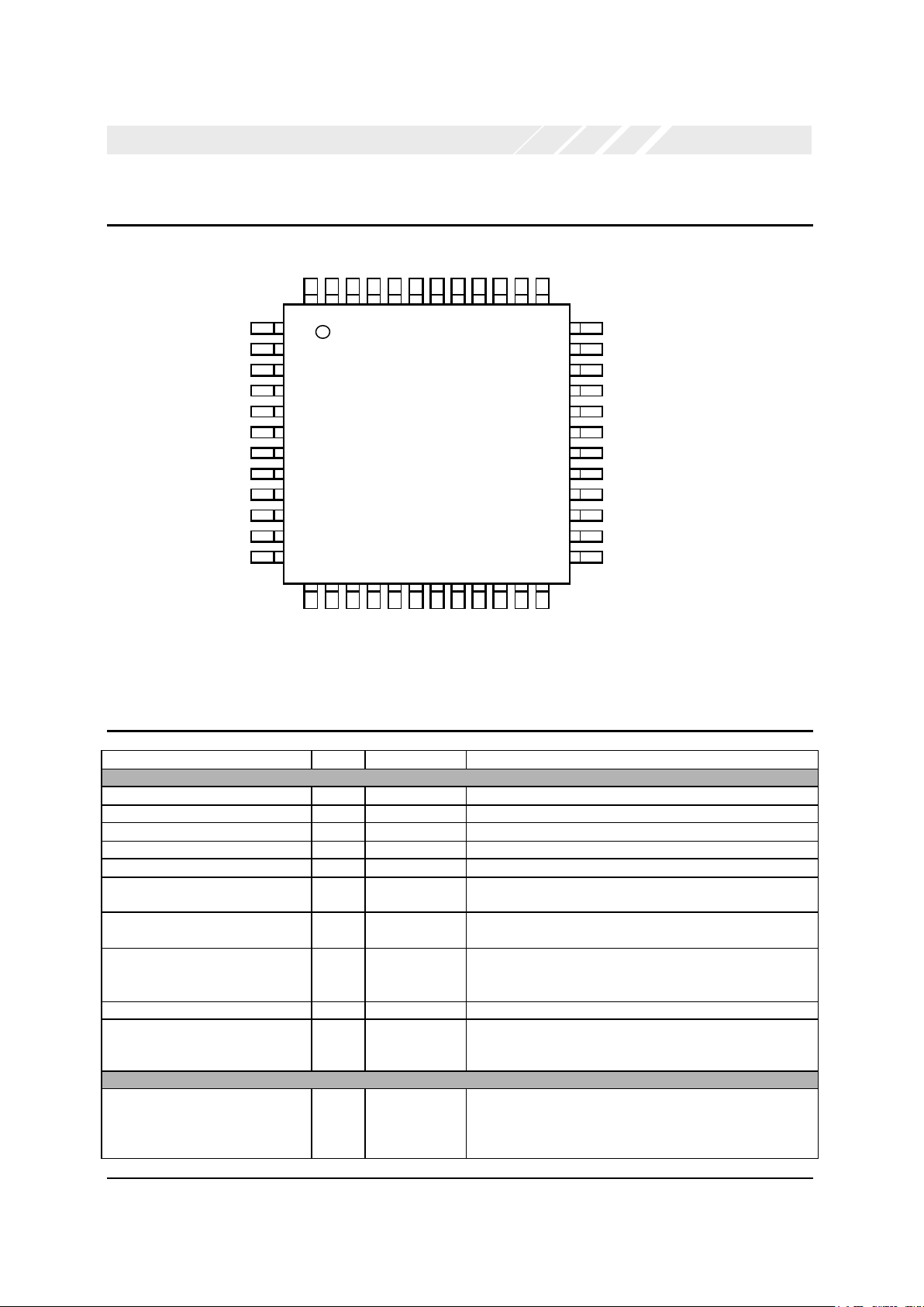
2 PIN INFORMATION
Figure 2: Pin Information
3 PIN DESCRIPTIONS
Pin Number Dir1 Name Description
CF/PCMCIA Interface and Control
46, 45, 43, 42 I A[3:0] PCMCIA/CF address bus, bits [3:0]
6, 7, 10, 11, 12, 37, 38, 41 I/O D[7:0] PCMCIA/CF data bi-directional bus.
44 IU REG# Register select and I/O enable
5 IU CE[1]# Active low card enable
4 I OE# Active low memory read enable
1 I WE# Active-low write enable used for strobing Memory Write data
(Attribute memory).
3 IU IORD# Active-low I/O read enable
2 IU IOWR# Active-low I/O write enable
32 O
O
WP
IOIS16#
Write protect (in Memory only mode)
Data is 16 bit (in IO and Memory mode)
47 IU RESET PCMCIA/CF Reset
48 O READY#
IREQ#
Device ready (in Memory only mode)
Active-low Interrupt request (in IO and Memory mode).
UART / Local Bus Function
24 O SOUT
IrDA_Out
UART serial data output.
UART IrDA data output when MCR[6] is set in enhanced
mode.
OX16CF950
IREQ#
RESETA3A2
REG#A1A0
D0
PWR
GND
D1
D2
Local Bus
Normal
4847464544434241403938
37
Mode
Mode
WE#
1 36
LB_WR#
/ A7
IOWR#
2 35
LB_RD#
/ A6
IORD#
3 34
LB_CS#
/ A5
OE#
4 33
LB_RST
/ A4
CE1#
5 32
IOIS16#
D7
6 31
MIO0
D6
7 30
RI#
GND
8 29
DCD#
PWR
9 28
DSR#
D5
10 27
CTS#
D4
11 26
DTR#
D3
12 25
RTS#
13 14 15 16 17 18 19 20 21 22 23 24
EE_CK
EE_CS
EE_DO
EE_DI
MODE
MIO1
GND
XTLI
XTLO
PWR
SIN
SOUT

Page 7
OXCF950 DATA SHEET V1.1
OXFORD SEMICONDUCTOR LTD.
23 I
SIN
IrDA_In
UART serial data input.
UART IrDA data input when IrDA mode is enabled (see
above).
29 I DCD# Active-low modem data-carrier-detect input.
26 O
DTR#
485_En
Tx_Clk_Out
Active-low modem data-terminal-ready output. If automated
DTR# flow control is enabled, the DTR# pin is asserted and
de-asserted if the receiver FIFO reaches or falls below the
programmed thresholds, respectively.
In RS485 half-duplex mode, the DTR# pin may be
programmed to reflect the state of the transmitter empty bit to
automatically control the direction of the RS485 transceiver
buffer (see register ACR[4:3]).
Transmitter 1x clock (baud rate generator output). For
isochronous applications, the 1x (or Nx) transmitter clock may
be asserted on the DTR# pin (see register CKS[5:4]).
25 O RTS# Active–low modem request-to -send output. If automated
RTS# flow control is enabled, the RTS# pin is de-asserted
and reasserted whenever the receiver FIFO reaches or falls
below the programmed thresholds, respectively.
27 I CTS# Active-low modem clear-to-send input. If automated CTS#
flow control is enabled, upon de-assertion of the CTS# pin,
the transmitter will complete the current character and enter
the idle mode until the CTS# pin is reasserted. Note: flow
control characters are transmitted regardless of the state of
the CTS# pin.
28 I DSR#
Rx_Clk_In
Active-low modem data-set-ready input. If automated DSR#
flow control is enabled, upon de-assertion of the DSR# pin,
the transmitter will complete the current character and enter
the idle mode until the DSR# pin is reasserted. Note: flow
control characters are transmitted regardless of the state of
the DSR# pin
External receiver clock for isochronous applications. The
Rx_Clk_In is selected when register CKS[1:0] = ’01’
30 I RI#
Tx_Clk_In
Active-low modem Ring-indicator input
External transmitter clock. This clock can be used by the
transmitter (and indirectly by the receiver) when register
CKS[6] = ‘1’.
21 O XTLO Crystal oscillator output
20 I XTLI Crystal oscillator input or external clock pin. Frequency
1.8MHz -> 60MHz
34 O
I
LBCS#
A[5]
Local Bus Mode : Active low local bus Chip select
Normal Mode : Address bit 5
35 O
I
LBRD#2
A[6]
Local Bus Mode : Active-low local bus read enable
Normal Mode : Address bit 6
36 O
I
LBWR
A[7]
Local Bus Mode : Active-low local bus write enable
Normal Mode : Address bit 7
33 O
LBRST2
A[4]
Local Bus Mode : Active high local bus Reset

Page 8
OXCF950 DATA SHEET V1.1
OXFORD SEMICONDUCTOR LTD.
I Normal Mode : Address bit 4
EEPROM
13 O EE_CK EEPROM clock.
14 O EE_CS EEPROM active-high Chip Select.
16 I EE_DI EEPROM data in. This pin should be pulled up using 1-10k
resistor.
15 O EE_DO EEPROM data out.
Miscellaneous Pins
18, 31 I/O MIO[1:0] User defined IO pins.
Note: that if enabled, MIO[1:0] can be used as an interrupt
inputs.
17 I MODE Local Bus mode select. Note Local Bus mode requires
indirect addressing, which is only supported by the PCMCIA
specification
‘0’ = Normal Mode (CF/PCMCIA compatible)
‘1’ = Local Bus Mode (PCMCIA compatible)
Power and Ground2
39, 19, 8 G GND Ground (0 Volts). The GND pins should be tied to ground
40, 22, 9 V VDD Power supply. The VDD pins should be tied to 5 Volts or 3.3
Volts
Table 1: Pin Descriptions
Note 1: Direction key:
I Input
IU Input with internal pull-up
ID Input with external pull-down
O Output
I/O Bi-directional
G Ground
V 3.3V/5V power

Page 9
OXCF950 DATA SHEET V1.1
OXFORD SEMICONDUCTOR LTD.
4 CONFIGURATION & OPERATION
PCMCIA and CF host systems allow for hot insertion of
cards.
Once a card has been inserted into a host system, the host
system will configure it. The PCMCIA standard defines two
card detect pins, that allow the host to be notified when a
card is inserted or removed.
By default the device will power up in either Normal or
Local Bus mode, depending on the mode pin. The
difference between these two modes is given in the
following table. Note that the Local Bus mode is not
suitable for CF systems.
Normal Mode (MODE=0) Local Bus Mode (MODE=1)
Address bus is 8 bits wide. Address bus is 4 bits wide.
Indirect access is not used. Indirect access is used.
No external local bus. External local bus supported.
Table 2: Differences between Normal & Local Bus Mode
The host system will wait for the READY# signal to be
active before reading the Card Information Structure, given
in attribute memory within the device. By reading this tuple
information, the host system is able to identify the device
type and the necessary resources requested by the device.
The host system will then load the device-driver software
according to this information and will configure the IO,
memory and interrupt resources. After determining that the
device is a memory and IO type device the host will enable
it’s IO mode by writing to the device’s Configuration
Options Register in attribute memory space. Device
drivers can then access the functions at the assigned
addresses.
A set of local configuration registers have been provided
that can be used to control the device’s characteristics
(such as interrupt handling) and report internal functional
status. These registers can be accessed in IO space,
utilising the same IO space as the local bus (Local Bus
mode only) and are situated above the UART registers.
These local registers can be set up by device drivers or
from the optional EEPROM.
The EEPROM can also be used to redefine the reset
values of all register areas to tailor the device to the end
users requirements if the default values do not meet the
specific requirements of the manufacturer. This reprogramming of the device can also be performed for the
CIS area, allowing the manufacturer to modify resources
required, or Manufacturer ID values for example. As an
additional enhancement, the EEPROM can be used to preprogram the UART, allowing pre-configuration, without
requiring device driver changes. This allows the enhanced
features of the integrated UART to be in place prior to
handover to any generic device drivers.
Note that a default set of tuples is provided for both
operating modes thus allowing for a single chip solution in
either mode.

Page 10
OXCF950 DATA SHEET V1.1
OXFORD SEMICONDUCTOR LTD.
5 PCMCIA / CF TARGET CONTROLLER
5.1 Operation
Note: See section 10 for timing waveforms.
The OXCF950 responds to a number of different
CF/PCMCIA accesses (detailed below). Section 11
contains timing diagrams and information for each of these
types of access.
• Direct Common Memory read/writes: These are
required in Local Bus mode only to allow indirect
access to attribute memory. This type of access is
permitted before and after configuration to allow the
reading of the CIS information, but is only supported
by the PCMCIA specification. Only 8 bit data, even
byte accesses are performed to this memory as it is
only used for access to the indirect attribute memory.
If the host attempts to access an invalid address, the
value of 0xFF (null) is returned.
• Direct Attribute Memory read/writes: Access to direct
attribute memory is required in both CF and PCMCIA
specifications. This memory space contains all the
configuration information for the device, as well as the
configuration registers. In CF systems, where only
direct access is permitted, this space is the only
memory space that is accessed by the host system. If
the host attempts to access common memory in this
mode, the device will return 0xFF telling the host that
there is no valid data in this space. In Local Bus
Mode, the direct attribute memory informs the host
that indirect access is enabled allowing the host to
perform indirect access to attribute memory, via
common memory. Valid data is 8 bits wide and on
even bytes only, for direct attribute memory (as
defined in the PCMCIA 7.1 standard)
• Indirect Attribute Memory read/writes (Local Bus mode
only): Access to indirect attribute memory is
performed through direct common memory. This
allows the device to provide full functionality with only
4 address pins. This access is performed to read the
CIS and also read/write to configuration registers.
Valid data is 8 bit wide and on even bytes only, for
indirect attribute memory (as defined in the PCMCIA
7.1 standard).
• IO read/writes: IO accesses are performed to access
the UART, local bus (Local Bus mode) and local
configuration registers. Data width is restricted to 8
bits, as required by the standard UART function. As
the device CIS information configures the card as a
single function device, no base addresses need to be
defined thus simplifying access to the function. As
reads and writes are immediate, there is no
requirement to hold the WAIT# signal in its active
state, thus providing maximum speed access to IO
space.
5.2 Configuration Space (Card Information
Structure)
5.2.1 Local Bus Mode Space Map
Direct Indirect
Main CIS either:
a) Normal Default
b) Bluetooth Default
c) Custom CIS
(downloaded from
EEPROM)
0xFF
Common
(Valid at even
locations only)
0x00
0x00 0x00
0xFF0xFF
0x00
0xFF
Indirect Access
Register
Hard Coded CIS to
link to indirect space
0x0F
0x10
0x0F
0x10
0x7F
0x80
Attribute
Function
Configuration
Registers
0xF6
0xF8
NOT VALID
NOT VALID
NOT VALID
Figure 3: Local Bus mode memory space map

Page 11
OXCF950 DATA SHEET V1.1
OXFORD SEMICONDUCTOR LTD.
Figure 4: Normal Mode memory space map
5.2.2 Normal Mode Space Map
5.3 Access to IO Function
5.3.1 Access to Internal UART
Access to the internal UART is achieved via standard IO
mapping. As the device is configured as a single function
device, no base address is required to access the UART.
As IO mapping is used, access to the UART is permitted
only after the card has been configured. Once the
Configuration Options Register has been set in the
Attribute area, the UART can be accessed following the
mapping shown in Table 3.
UART Address (hex) CF/PCMCIA offset from
address 0 for UART
function in IO space (hex)
0 0
1 1
2 2
3 3
4 4
5 5
6 6
7 7
Table 3: UART's mapping in I/O space
5.3.2 Access to Local Bus
Access to the internal Local Bus is achieved via standard
IO mapping. The Local Bus function is available in Local
Bus mode only as it’s device pins are used as the extended
address bits required for direct access in Normal mode.
Indirect access is only supported in the PCMCIA
specification, so the local bus is only available in PCMCIA
systems. As the device is configured as a single function
device, no base address is required to access the Local
Bus. As IO mapping is used, access to the Local Bus is
permitted only after the card has been configured. Once
the Configuration Options Register has been set in the
Attribute area, the Local Bus can be accessed following the
mapping shown in table Table 4. This access is permitted
only if bit[0] is reset to ‘0’ in the MDR register in the UART,
otherwise the local configuration registers will be accessed
rather than the local bus.
Local Bus Address1 (hex) CF/PCMCIA offset from
address 0 for Local Bus
function in IO space (hex)
0 8
1 9
2 A
3 B
4 C
5 D
6 E
7 F
Table 4: Local Bus mapping in I/O space
Note 1: Although only 4 bits of IO address space are
requested by the default CIS in the device, the address
range may be extended past these four bits. This can be
achieved by modifying the CIS, via the EEPROM, and
connecting the extended address bits to the external local
bus device.
Direct Indirect
Main CIS either:
a) Normal Default
b) Bluetooth Default
c) Custom CIS
(downloaded from
EEPROM)
0xFF
Common
(Valid at even
locations only)
0x00
0x00 0x00
0xFF0xFF
0x00
0xFF
Attribute
Additional Storage
Space, which can be
downloaded from the
EEPROM.
0x7F
0x80
Function
Configuration
Registers
0xF8
0xF6
NOT VALID
NOT VALID
NOT VALID

Page 12
OXCF950 DATA SHEET V1.1
OXFORD SEMICONDUCTOR LTD.
5.3.3 Accessing Local Configuration Registers
The local configuration registers are a set of device specific registers, which can be accessed via standard IO mapping. As the
device is configured as a single function device, no base address is required to access the local configuration registers. Since IO
mapping is used, access to the local configuration registers is permitted only after the card has been configured. Once the
Configuration Options Register has been set in the Attribute area, the local configuration registers can be accessed following the
mapping shown in Table 5. This access is always permitted in Normal Mode. In Local Bus Mode access is only permitted if bit[0]
is set to ‘1’ in the MDR register in the UART, otherwise the local bus will be accessed rather than the local configuration
registers.
CF/PCMCIA offset from address 0 for local
configuration registers in IO space (hex)
Register Map
8 EEPROM Status and Control register
9 Multi-Purpose I/O Configuration register
A UART Divider/Interrupt Pulse Width Divider register
B Mode Status register
C Interrupt Status register
D Soft UART/Local Bus reset register
E Reserved
F Reserved
Table 5: Local Configuration Register's mapping in I/O space
Each of the local configuration registers are explained in the following sections
EEPROM Status and Control register ‘ESC’(Offset 0x08)
This register defines the control on the serial EEPROM. The individual bits are described in Table 6.
Read/Write Bits Description
EEPROM PCMCIA
Reset
7:5 Reserved - R 000
4 EEPROM Data In.
For reads from the EEPROM this input bit is the output-data (DO) of the
external EEPROM connected to EE_DI pin
- R X
3 EEPROM Data Out.
For writes to the EEPROM, this output bit feeds the input-data of the
external EEPROM (DI). This bit is output on the devices EE_DO and
clocked into the EEPROM by EE_CK
- R/W 0
2 EEPROM Clock.
For reads or writes to the external EEPROM toggle this bit to generate an
EEPROM clock (EE_CK pin)
- R/W 0
1 EEPROM Chip Select.
When ‘1’ the EEPROM chip select pin EE_CS is activated (high). When ‘0’
EE_CS is de-activated (low)
- R/W 0
0 EEPROM Valid
A ‘1’ indicates that a valid EEPROM program header is present
- R X
Table 6: EEPROM Status and Control Register

Page 13
OXCF950 DATA SHEET V1.1
OXFORD SEMICONDUCTOR LTD.
Multi-Purpose I/O Configuration register ‘MIC’ (Offset 0x09)
This register configures the operation for the multi-purpose I/O pins ‘MIO[1:0]’ as follows
Read/Write Bits Description
EEPROM PCMCIA
Reset
7:4 Reserved - R 0000
3:2 MIO1 Configuration register
00 -> MIO1 is a non-inverting input pin
01 -> MIO1 is an inverting input pin
10 -> MIO1 is an output pin driving ‘0’
11 -> MIO1 is an output pin driving ‘1’
W R/W 00
1:0 MIO0 Configuration register
00 -> MIO0 is a non-inverting input pin
01 -> MIO0 is an inverting input pin
10 -> MIO0 is an output pin driving ‘0’
11 -> MIO0 is an output pin driving ‘1’
W R/W 00
Table 7: Multi Purpose I/O Configuration Register
UART Divider/Interrupt Pulse Width Divider register ‘DIV’ (Offset 0x0A)
This register defines the divide values (2^N division) for the clocks to the UART and Interrupt pulse generator signal. This allows
the device to be set up in its lowest power mode possible, and is fully programmable by the host or the EEPROM. The default
value for the UART clock divider provides a clock to the UART of x1. The default value for the Interrupt pulse divider provides a
clock to the interrupt processor of /32. See Section 5.4.1 Note that the UART clock rate should not be changed without then
resetting the UART(see SRT register).
Read/Write Bits Description
EEPROM PCMCIA
Reset
7:6 Reserved - R 00
5:3 Uart clock divide value.
The division ratio is 2^N, giving 1, 2, 4, 8, 16, 32, 64, 128
W R/W 000
2:0 Interrupt Pulse divide value:
This field should be set under the following clock freq. conditions
000 -> when clock frequency is less than 2MHz
001 -> when clock frequency is between 2 and 4MHz
010 -> when clock frequency is between 4 and 8MHz
011 -> when clock frequency is between 8 and 16MHz
100 -> when clock frequency is between 16 and 32MHz
101 -> when clock frequency is between 32 and 64MHz
110 -> RESERVED
111 -> RESERVED
W R/W 101
Table 8: UART Divider/ Interrupt Pulse Width Divider
Mode Status register ‘MSR’ (Offset 0x0B)
This read only register return the state of the MODE pin (i.e. whether in Normal or Local Bus modes).
Read/Write Bits Description
EEPROM PCMCIA
Reset
7:1 Reserved - R 0000000
0 Mode
O = Normal, 1 = Local Bus
- R X
Table 9: Mode Status Register

Page 14
OXCF950 DATA SHEET V1.1
OXFORD SEMICONDUCTOR LTD.
Interrupt Status and Control register ‘ISR’ (Offset 0x0C)
This register controls the assertion of interrupts from the User I/O pins (MIO[1:0]) as well as returning the internal status of the
interrupt sources.
Read/Write Bits Description
EEPROM PCMCIA
Reset
7:5 Reserved - R 000
4 UART Interrupt status
This bit reflects the state of the internal UART interrupt
- R 0
3 MIO[1] interrupt mask
When set to ‘1’ allows pin MIO[1] to assert an interrupt on the devices
IREQ# pin. The state of the MIO[1] signal that causes an interrupt is
dependent upon the polarity set by the register fields MIC[3:2].
W R/W 0
2 MIO[0] interrupt mask
When set to ‘1’ allows pin MIO[0] to assert an interrupt on the devices
IREQ# pin. The state of the MIO[0] signal that causes an interrupt is
dependent upon the polarity set by the register fields MIC[1:0].
W R/W 0
1 MIO1 Internal state
This bit reflects the state of the internal MIO[1]. The internal MIO[1] signal
reflects the non-inverted or inverted state of MIO[1] pin
- R X
0 MIO0 Internal state
This bit reflects the state of the internal MIO[0]. The internal MIO[0] signal
reflects the non-inverted or inverted state of MIO[0] pin
- R X
Table 10: Interrupt Status Register
Soft UART/Local Bus reset register ‘SRT’ (Offset 0x0D)
This register controls the soft reset passed to the UART and local bus reset. These reset lines are in addition to the soft reset
that may be produced by the host (bit[7] of the COR register in attribute memory space). Note that the local bus reset is used in
Local Bus mode only and not in Normal mode. Note these bits are not self-clearing.
Read/Write Bits Description
EEPROM PCMCIA
Reset
7:2 Reserved - R 000000
1 Active high soft reset for UART W R/W 0
0 Active high soft reset for Local Bus W R/W 0
Table 11: Soft UART / Local Bus Reset (LB reset used in Local Bus Mode only)
5.4 CF / PCMCIA Interrupt
5.4.1 Interrupt Generation
PCMCIA/CF cards support pulse or level type interrupt signals to request interrupt service from the host system. The CIS of the
card specifies whether pulse, level or both types of interrupt can be generated. Once the host has read the CIS it is able to set
the LevlReq field in the Configuration Options Register (COR) to tell the card which type of interrupts should be generated.
The OXCF950 is capable of generating either type of interrupt. However, to reduce power consumption, the default CIS states
that only level type interrupts can be generated. A custom CIS can be constructed that specifies the card has the ability to
generate pulse type interrupts, if this is required, by using an external EEPROM.
The OXCF950 uses a programmable clock divider circuit to generate pulse type interrupts signals. The pulse that is generated is
one clock cycle (after division) in length. The divider circuit can be programmed by setting the contents of the Interrupt Pulse
Page 15
OXCF950 DATA SHEET V1.1
OXFORD SEMICONDUCTOR LTD.
Divide Value field in the DIV local configuration register (see section 6.3.4.3). This allows the length of the pulse to be varied, so
that different clock frequencies can be used and the pulse can still be kept as short as possible, without violating the minimum
length of 50 µs as defined in the PCMCIA Standard. Table 12 shows how the register should be programmed for different clock
frequencies.
Clock Frequency (MHz) Interrupt Divider Setting
f < 2 000
2 <= f < 4 001
4 <= f < 8 010
8 <= f < 16 011
16 <= f < 32 100
32 <= f < 64 101
110
RESERVED
111
Table 12: Interrupt Pulse Divide Value settings
5.4.2 Interrupt Sources
The OXCF950 has three possible interrupt sources. These are the internal UART, and the two multi-purpose I/O pins, which can
be configured as interrupts using the MIO Configuration Register (MIC – see section 6.3.4.2) and the Interrupt Status and Control
Register (ISR – see section 6.3.4.5)
When the OXCF950 is requesting interrupt service, the Intr field within the Configuration Status Register (CSR – see section
6.5.2) will be set to 1. Otherwise this field will be cleared to 0. The Intr field value is controlled by the interrupt source (i.e UART
or MIO [1:0]). The status of the actual interrupts can be read from the ISR register.
5.5 CF/PCMCIA Function Configuration Registers
Each PCMCIA/CF card’s I/O function must implement Function Configuration Registers (FCR). These registers allow the host to
configure the function provided by the card, and are mapped into the attribute memory space at the location specified within the
CONFIG tuple (in the CIS). The CONFIG tuple defines a base address for the Function Configuration Registers and a number
corresponding to how may registers are supported (4 registers in the OXCF950). Each of these registers has read/write
capability and is mapped at even location, consistent with the design of attribute memory. The registers supported in the
OXCF950 are shown in the following table.
Offset from
FCR base
address
Attribute
memory address
Register
0 F8 Configuration Options Register
2 FA Configuration and Status Register
4 FC Pin Replacement Register
8 FE Socket & Copy Register
Table 13: Configuration Register Mapping
Due to the type of function the OXCF950 configures the card to be, and the fact that it is a single function device, only a sub-set
of the total number of configuration registers are required.
The definition of each configuration register is detailed in the next few sub-sections.

Page 16
OXCF950 DATA SHEET V1.1
OXFORD SEMICONDUCTOR LTD.
5.5.1 Configuration Options Register ‘COR’ (offset 0xF8)
The configuration options register is used to configure PCMCIA/CF cards that have programmable address decoders. Once the
card’s client driver has successfully parsed the CIS, it will attempt to obtain system resources, as requested by the CIS. On
completion of this it assigns the resources to the card via the COR. The COR format and description is given in Table 14.
D7 D6 D5 D4 D3 D2 D1 D0
SRESET LevIREQ Function Configuration Index
Field Type Description
SRESET R/W Software reset
Setting this field to ‘1’ places the card in the reset state. This is equivalent to
setting the RESET signal (on pin) except this SRESET field is not reset.
Returning this field to ‘0’ leaves the card in the same un-configured, reset state
as the card would be following a power-up and hard reset.
LevIREQ
1
R/W Level Mode IREQ#
Setting this field to ‘1’ enables level type interrupts
Setting this field to ‘0’ enables pulse type interrupts
Function Configuration Index R/W Configuration Index
The host sets this field to the value of the Configuration Entry Number field of a
Configuration Table Entry tuple as defined in the CIS. On setting the non-zero
value in this field the function IO is enabled and IO accesses are allowed. When
the field is set to zero (e.g. after a hard reset) the card will be configured to
memory only mode and all IO accesses will be ignored by the card.
Table 14: Configuration Option Register
Note 1
The default tuples in the CIS tell the host that only level type interrupts are supported to allow lowest power consumption. The
OXCF950 supports both level and pulse type interrupts, and if a particular manufacturer requires to use pulse type, or both, then
the CIS can be modified using the external EEPROM.
5.5.2 Configuration Status Register ‘CSR’ (Offset 0xFA)
The Configuration and Status Register is an optional register, supported by the OXCF950. The register allows additional control
over a function’s configuration and reports status related to the function’s configuration.
D7 D6 D5 D4 D3 D2 D1 D0
Changed SigChg IOIs8 RFU Audio PwrDwn Intr IntrAck
Field Type Description
Changed R If a PCMCIA/CF card is using the I/O interface, the function’s Pin Replacement
register is present and one or more of the state change signals in the Pin
Replacement Register are set to one(1), or one Event bits in the Extended Status
Register are set (1) and the corresponding Enable bit is set (1), the function shall
set this field to one (1).
If a PCMCIA/CF card is not using the I/O interface or the function’s Pin
Replacement register is not present, this field is undefined and should be
ignored.
SigChg
1
R/W This field serves as a gate for STSCHG#
If a PCMCIA/CF card is using the I/O interface and both the Changed and
SigChg fields are set to one (1), the function shall assert STSCHG#.

Page 17
OXCF950 DATA SHEET V1.1
OXFORD SEMICONDUCTOR LTD.
If a PCMCIA/CF card is using the I/O interface and this field is reset to zero (0),
the function shall not assert STSCHG#.
If a PCMCIA/CF card is not using the I/O interface or the function’s Pin
Replacement register is not present, this field is undefined and should be
ignored.
IOIs8 R/W The host sets this field to one (1) when it can provide I/O cycles only with an 8-bit
D[7..0] data path. The card is guaranteed that accesses to the 16-bit registers will
occur as two byte accesses rather than as a single 16-bit access.
RFU - Reserved. Must be zero (0).
Audio2 R/W This bit is set to one (1) to enable audio information on SPKR# when the card is
configured.
PwdDwn3 R/W When the host sets this field to one (1), the function shall enter a power-down
state, if such a state exists.
If a PCMCIA/CF card function does not have a power-down state, the function
shall ignore this field.
Intr R Interrupt Request / Acknowledge – This field reports whether the function is
requesting interrupt servicing and may be used to acknowledge the host system
is ready to process another interrupt request from the PCMCIA/CF card.
The function shall set this field to one (1) when it is requesting interrupt service.
The function shall set this field to zero (0) when it is not requesting interrupt
service.
Writes to this field are ignored when the IntrAck field of all Configuration and
Status Registers on the PCMCIA/CF card are reset to zero (0).
IntrAck R/W Single function cards ignore this field on writes and always return zero (0).
Table 15: Configuration Status Register
Note 1
The STSCHG# signal is optional and is not supported on the OXCF950, to reduce the complexity of the device.
Note 2
Audio is not supported on the device.
Note 3
The OXCF950 does not support a specific power down mode, since it is a low power device that features a number of sleep
modes (see Section 7 for further details).
5.5.3 Pin Replacement Register ‘PRR’ (Offset 0xFC)
The Pin Replacement Register is implemented to provide information about READY, WP or the BVD[2..1] status when
implementing the I/O interface.
D7 D6 D5 D4 D3 D2 D1 D0
CBVD1 CBVD2 CREA DY CWProt RBVD1 RBVD2 RREADY RWProt
Field Description
CBVD1 This bit is set (1) when the corresponding bit, RBVD1, changes state. This bit may also be
written by the host.
CBVD2
This bit is set (1) when the corresponding bit, RBVD2, changes state. This bit may also be

Page 18
OXCF950 DATA SHEET V1.1
OXFORD SEMICONDUCTOR LTD.
written by the host.
CREADY This bit is set (1) when the corresponding bit, RREADY, changes state. This bit may also be
written by the host.
CWProt This bit is set (1) when the corresponding bit, RWProt, changes state. This bit may also be
written by the host.
RBVD1 When read, this bit represents the internal state of the Battery Voltage Detect circuits which
would be on the BVD1 pin.
When this bit is written as 1 the corresponding CBVD1 bit is also written. When this bit is
written as 0, the CBVD1 bit is unaffected.
RBVD2 When read, this bit represents the internal state of the Battery Voltage Detect circuits which
would be on the BVD2 pin.
When this bit is written as 1 the corresponding CBVD2 bit is also written. When this bit is
written as 0, the CBVD2 bit is unaffected.
RREADY When read, this bit represents the internal state of the READY signal. This bit may also be
used to determine the state of READY as that pin has been relocated for use as Interrupt
Request on IO Cards.
When this bit is written as 1 the corresponding “changed” bit is also written. When this bit is
written as 0, the “changed” bit is unaffected.
RWProt When read, this bit represents the state of the WP signal. This signal may also be used to
determine the state of the Write Protect switch when pin 33 is being used for IOIS16#.
When this bit is written as 1 the corresponding “changed” bit is also written. When this bit is
written as 0, the “changed” bit is unaffected.
Table 16: Pin Replacement Register
5.5.4 Socket and Copy Register ‘SCR’ (Offset 0xFE)
This is an optional read/write register, implemented by the OXCF950, which the PCMCIA/CF card may use to distinguish
between similar cards installed in a system. This register is always written by the system before writing the card's Function
Configuration Index field in the Configuration Option register.
D7 D6 D5 D4 D3 D2 D1 D0
Reserved Copy Number Socket Number
Field Description
Reserved This bit is reserved for future standardization. This bit must be set to zero (0) by software when
the register is written.
Copy Number PCMCIA/CF cards that indicate in their CIS that they support more than one copy of identically
configured cards, should have a copy number (0 to MAX twin cards, MAX = n-1) written back
to the socket and Copy register.
This field indicates to the card that it is the n’th copy of the card installed in the system, which
is identically configured. The first card installed receives the value 0. This permits identical
cards designed to share a common set of I/O ports while remaining uniquely identifiable and
consecutively ordered.
Socket Number This field indicates to the PCMCIA/CF card that it is located in the n’th socket. The first socket
is numbered o. This permits any cards designed to do so to share a common set of I/O ports
while remaining uniquely identifiable.
Table 17: Socket and Copy Register
 Loading...