

Page 1

Intelligent CCFL Inverter Controller
FEATURES
• Supports wide-range voltage input
applications (8v to 20v)
• Built-in intelligence to manage ignition and
normal operation of CCFLs
• Reduces the number of components and
board size by 30% compared with
conventional designs
• 85% efficiency vs. typical 70% efficiency of
conventional designs
• Zero-voltage-switching full bridge topology
• Built-in internal open-lamp and over-voltage
protections
• Integrated burst mode control, and wide
dimming range (10% to 100%) with
integrated burst mode control
• Supports multiple CCFL lamps
• Simple and reliable 2-winding transformer
design
• Constant-frequency design eliminates
interference with LCDs
• Low stand-by power
ORDERING INFORMATION
OZ960S - 20-pin plastic SSOP 150mil
OZ960IS - 20-pin plastic SSOP 150mil
OZ960G - 20-pin plastic SOP 300mil
OZ960IG - 20-pin plastic SOP 300mil
OZ960D - 20-pin plastic DIP 300mil
OZ960ID - 20-pin plastic DIP 300mil
GENERAL DESCRIPTION
The OZ960 is a unique, high-efficiency, Cold
Cathode Fluorescent Lamp (CCFL) backlight
inverter controller that is designed for wide input
voltage inverter applications. Additionally, the
OZ960 performs the lamp dimming function with
an analog voltage or low frequency Pulse Width
Modulation (PWM) control.
Operating Principle:
Operating in a zero-voltage switching, full-bridge
configuration, the inverter circuit achieves a very
high efficiency power conversion. In addition, the
transformer in the OZ960 does not require any
specific gap-less arrangement. The simple, low
cost transformer provides designers a high
degree of design flexibility in specifying
transformers. Setting the switching frequency
higher than the resonant frequency of a highquality-factor resonant tank circuit yields a good-
OZ960
quality waveform received, at the CCFL voltage
and current.
The OZ960 operates at a single, constant
frequency in a phase-shift PWM mode. Intelligent
open-lamp and over-voltage protections provide
design flexibility so various transformer
models/manufacturers may be used. The built-in
burst mode control provides a wide dimming
range and simplifies the application circuit
designs. Both operating and burst-mode
frequencies are user-programmable parameters.
The single stage design results in a low cost,
reliable transformer without expensive, less
reliable secondary fold-back treatment. The
transformer does not require a more expensive
center tapped primary.
The OZ960 is available in a 20-pin SSOP
package. It is specified over the commercial
temperature range of 0°C to +70°C, and the
industrial temperature range of -40°C to +85°C.
FUNCTIONAL BLOCK DIAGRAM
Refer to the functional block diagram in Figure 2,
page 3, and the Pin Description Table on page 4.
A precision reference provides a reference
voltage for both internal and external uses. An
oscillator circuit generates a user-programmable
operating frequency with an external capacitor
and a timing resistor. In addition, another resistor
to program striking frequency is provided. The
drive circuit consists of four outputs. These are
designed to achieve zero-voltage switching, fullbridge applications. An error amplifier is provided
to regulate the CCFL current. The Soft-start
circuit offers a gradual increase of the power to
the CCFL during the ignition period. The overvoltage protection block offers a regulated
striking voltage for CCFLs. The striking time is
programmable simply through an external
component. The open-lamp protection is
integrated in the protection block. This block
intelligently differentiates the striking condition
and open-lamp condition. ENA circuitry enables
the operation of the IC through a TTL signal
interface. Wide-dimming control is achieved
through the burst-mode control block.
10/23/01 OZ960-DS-1.6 Page 1
Copyright 2000 - 01 by O2Micro All Rights Reserved U.S. Patent #6,259,615
Page 2
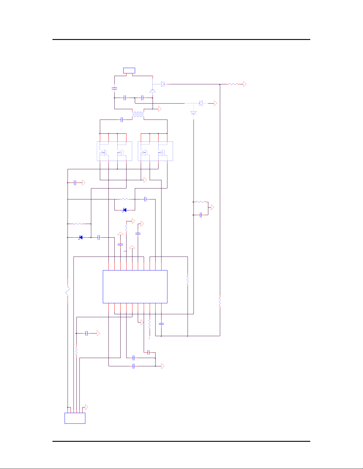
TYPICAL APPLICATION CIRCUIT
F1
FUSE 1A
J1
C4
100P
7
8
U1
Si5504
2
1
C1
10U
5.1K
R2
C3
4.7V
D1
R1
Vin
VIN
DIM
ENA
GND
5VDC
0.047u
20
U2
OZ960
1
C2
1.0u
22
Figure 1: An 8-22V Application Circuit of OZ960
J2
C7
C6
2.2U
6
QB
3
4 5
R3
D2
R4
52.3K
C5
220P
1817161514
CT
PDR_A
NDR_B
CTIMR
OVP
ENA
23456
1
RT
SST
22P
QA
10K
4.7V
RT
2
PGND
VDDA
C9
C8
C11
T1
0.47u
1.0u
0.033U
32:2200
8
1
C12
C10
LCT
DIM
GNDA
REF
7199
7
2
0.047u
6.8nF
138
LPWMRT1
RT
C13
QD
R5240K
12
PDR_C
FB
0.1u
CR1
BAV99L
6
QC
U3
3
4 5
11
NDR_D
CMP
10
C14
0.015u
OZ960
499
R9
CR2
Si5504
R6 33k
BAV99L
R7
1M
C15
0.1u
R8
51k
VIN: 8.0V---22V
ENA: 0V--1.0V Disable;2.0V---3.3V Enable
DIM: 3V Max. Brightness; 1.2V Min. Brightness
Striking frequency: 74KHz - 82KHz
Operating frequency: 56KHz - 64KHz
OZ960-DS-1.6 Page 2
Page 3
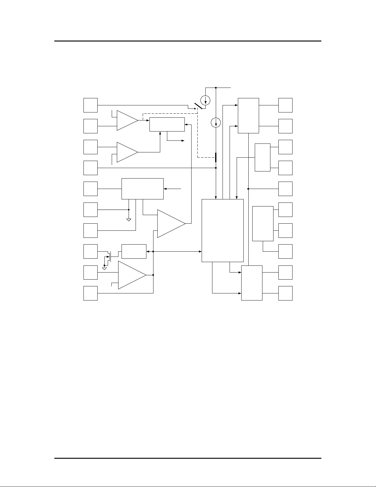
CTIMR
OVP
ENA
ACTIVE
"HIGH"
SST
OZ960
I=3uA
1
2V
+
2
3
4
OVP
-
hys.
COMP
+
ENA
-
hys.
1.5V
COMP
Protection
POFF
I=6uA
Soft
Start
NDR_B
PDR_A
HF
OSC
20
19
18
17
NDR_B
PDR_A
CT
RT
VDDA
GNDA
REF
RT1
FB
CMP
10
5
6
7
8
9
1.25V
Reference
2.75V
2.50V
Ignition
EA
+
POFF
OPLAMP
+
ZVS
Phase-Shift
Controller
PDR_C
NDR_D
BurstMode
Control
16
15
14
13
12
11
PGND
LCT
DIM
LPWM
PDR_C
NDR_D
Figure 2. Functional Block Diagram
OZ960-DS-1.6 Page 3
Page 4
OZ960
PIN DESCRIPTION
Names Pin No. I/O Description
CTIMR 1 I Capacitor for CCFL ignition duration
OVP 2 I Output voltage sense Vth=2.0V
ENA 3 I Enable input; TTL signal is applicable
SST 4 I Soft-start capacitor
VDDA 5 I Voltage source for the IC
GNDA 6 I Analog signal ground ref erence
REF 7 O Reference voltage output; 2.5V typical
RT1 8 I Resistor for programming ignition frequency
FB 9 I CCFL current feedback signal
CMP 10 O Compensation output of the current error amplifier
NDR_D 11 O NMOSFET drive output
PDR_C 12 O PMOSFET drive output
LPWM 13 O Low-frequency PWM signal f or burst-mode dimmi ng control
DIM 14 I Input analog signal for burst-m ode di mming control
LCT 15 I Triangul ar wave for burst-mode dimming; frequency
PGND 16 I Power ground reference
RT 17 I Timing res i stor set operating frequency
CT 18 I Timing c apacitor set operating frequency
PDR_A 19 O P MOSFE T dri ve output
NDR_B 20 O NMOSFET drive output
ABSOLUTE MAXIMUM RATINGS WITH RESPECT TO INPUT POWER SOURCE RETURN REFERENCE
VDDA 7.0V
GNDA, PGND +/- 0.3V
Logic inputs -0.3V to VDD +0.3V
OZ960
Operating temp. 0oC to 70oC -40oC to 85oC
Operating junction temp.
Storage temp. -55 oC to 150 oC
150 oC
OZ960I
RECOMMENDED OPERATING RANGE
VDDA
Fosc 30 KHz to 150 KHz
Rosc 50 k to 150 k
(1)
Note
: The “Absolute Maximum Ratings” are those values beyond which the safety of the devic e cannot be guaranteed.
The device should not be operated at these limits. The “Functional Specifications” table w ill def ine the conditions for
actual device operation. Exposure to absolute maximum rated condit i ons for extended periods may affec t device
reliability.
4.7V ~ 5.5V
(1)
OZ960-DS-1.6 Page 4
Page 5

OZ960
FUNCTIONAL SPECIFICATIONS
Parameter Symbol Test Conditions Limits Unit
VDDA=5V; Tamb = 25oC Min Typ Max
Reference Voltage
Nominal voltage Vref I
Line regulation VDDA = 4.7V – 5.3V - 4 - mV/V
Load regulation I
High Frequency Oscillator
Initial accuracy fosc CT = 100pF, RT = 120k
Ramp peak - 3.0 - V
Ramp valley - 1.0 - V
Temp. stability TA = 0 oC to 70oC - 200 - ppm/ oC
Low Frequency Oscillator
Initial accuracy
Ramp peak 2.85 3.0 3.15 V
Ramp valley 0.94 1.0 1.06 V
Low Frequency PWM
Duty Cycle Range 0 - 100 %
Error Amplifier
Input offset voltage - 7 - mV
Input voltage range 0 - VDD-1. 5V V
Offset current at FB pin - - 100 nA
Reference voltage at non-
inverting input pin (internal)
Open loop voltage gain - 80 - dB
Unity gain bandwidth - 1.0 - MHz
Power supply rejection - 60 - dB
Threshold
Over Voltage Protection 1.90 2 2.15 V
Supply
Supply current I
Supply current ION
SST current
CTIMR current
NDR-PDR Output
Output resistance Rp Current source - 27 Output resistance Rn Current sink - 14 -
= 0.1mA 2.37 2.5 2.63 V
load
= 0.025 mA to 0.25 m A - 2 - mV/mA
load
(1)
V
1.19 1.25 1.31 V
ADJ
ENA = low - 150 200
OFF
ENA = high; VDDA = 5V;
Vdim = 2V; LPWM = 50k
Ca=Cb=Cc=Cd=2nF
HF = 60kHz; LF = 185Hz
(2)
(3)
57 60 KHz
5533
See Table 1, page 6
µA
- 4.4 5.5 mA
See Table 1, page 6
See Table 1, page 6
Ω
Ω
OZ960-DS-1.6 Page 5
Page 6

Parameter Symbol Test Conditions Limits Unit
Max. / Min. Overlap
VDDA = 5V ; Tamb = 25oC Min Typ Max
Min. Overlap between
diagonal switches
Max. Overlap between
diagonal switches
Brake before Make
PDR_A / NDR_B
PDR_C / NDR_D
Parameter Symbol Test Conditions
Low Frequency Oscillator
Initial accuracy
Supply
SST current
CTIMR current
Brake before Make
PDR_A / NDR_B
PDR_C / NDR_D
Threshold
Enable
fosc
I
SST
I
CTIMR
OZ960
LCT = 6.8nF, LPWM = 50k
HF = 60kHz 250 380 530 ns
HF = 60kHz 250 380 520 ns
HF = 60kHz
Ca=Cb=Cc=Cd=2nF
HF = 60kHz
Ca=Cb=Cc=Cd=2nF
(3)
(3)
1.35 1.50 1.65 V
Min Typ Max Min Typ Max
(2)
160 220 250 Hz
4.9 7.5 10
2.2 3.3 4.5
3.0 4.5 5.5
78 81 84
See Table 1, below
See Table 1, below
Limits
Unit
µA
µA
OZ960
%
%
OZ960I
Limits
220 340 Hz
150
4.9 6.0 12
2.0 3.0 5.2
250 380 565 ns
250 380 545 ns
1.25 1.50 1.65 V
Unit
µA
µA
(1)
Note
CT: capacitor from CT (P i n 18) t o ground
RT: resistor from RT (P in 17) to ground
(2)
Note
LCT: capacitor from LCT (Pi n 15) to ground
LPWM: resis tor from LPW M (Pi n 13) to ground
(3)
Note
Ca: capacitor from PDR_A (Pin 19) to VDDA
Cb: capacitor from NDR_B (Pin 20) to ground
Cc: capacitor from PDR_C (Pin 12) to VDDA
Cd: capacitor from NDR_D (Pin 11) to ground
Table 1. Low Frequency Oscillator, Supply and Brake
before Make Specifications for OZ960 and OZ960
I
OZ960-DS-1.6 Page 6
Page 7

FUNCTIONAL INFORMATION
1. Steady-State Operation
Refer to the schematic shown in Figure 1, the
OZ960 drives a full-bridge power train where the
transformer couples the energy from the power
source to the secondary CCFL load. The
switches in the bridge denoted as QA, QB, QC
and QD are configured such that QA and QB, QC
and QD are turned on complementarily. The
duration of QA and QD, QB and QC turn on
simultaneously determines an amount of energy
put into the transformer which in turn delivers to
the CCFL. The current in CCFL is sensed via
resistor R9 and regulated through the adjustment
of the turn-on time for both diagonal switches.
This is accomplished through an error amplifier in
the current feedback loop. A voltage loop is also
established to monitor the output voltage so that
a programmable striking voltage is achieved. The
OVP represents the peak-detect signal of the
voltage on the output of the transformer. A softstart circuit ensures a gradual increase in the
input and output power. The soft-start capacitor
determines the rate of rise of the voltage on SST
pin where the voltage level determines the ontime duration of QA and QD, QB and QC
diagonal switches. This minimizes the surge
impacts in circuit designs.
Apply enable signal to the ENA pin of the IC after
the bias voltage applied to VDDA initiates the
operation of the circuit. The output drives, include
PDR_A, NDR_B, PDR_C and NDR_D put out a
complementary square pulse. The frequency is
determined by R4 and C5 where they are
connected to RT and CT pins respectively.
Initially, the energy converted from the power
source to the CCFL is low due to the soft start
function. It increases as soft start capacitor
voltage increases linearly with time. The voltage
at the secondary side of the transformer T1
increases correspondingly. This process
continues until the CCFL current is detected and
reaches a regulated value. The output of the
error amplifier, CMP, follows the feedback signal,
commands a proper switching among the four
output drives to maintain current regulation. The
operations of the four switches are implemented
with zero-voltage-switching to provide a highefficiency power conversion.
In the case of open-lamp condition, the OZ960
provides a programmable striking-frequency
intelligence to optimize the ignition scheme. This
is implemented through resistor R5. Effectively,
R5 is in parallel with R4 to yield a required
striking frequency. In addition, the striking time is
also programmable through the capacitor C8.
Striking voltage, or the open-lamp voltage, is
OZ960
regulated through a voltage feedback loop where
output voltage is monitored. The signal, being
sent to the OVP pin, commands the output drives
to provide the desired output voltage. This design
provides high degree of flexibility while
maintaining OZ960 a very high integration
device.
One protection feature needed is removing the
lamp during normal operation. The OZ960
senses the missing current signal through current
amplifier, it shuts off the output drives and stay in
the latched mode. This is differentiated
intelligently with turning on the inverter while
CCFL is not connected. Recycle of the IC power
is necessary to resume normal operation.
Dimming control: dimming control of the inverter
is implemented by adjusting the amount of
energy processed and delivered to the CCFL. A
PWM burst-mode scheme is internally generated
which provides 0% to 100% wide dimming
control. An input analog voltage signal is fed into
DIM pin and determines the dimming level of the
CCFL. The burst-mode frequency is
programmable through a capacitor C10 as shown
in the schematic.
The OZ960 inverter operates in a constant
frequency mode. This eliminates any undesired
interference between inverter and LCD panels
where the interference is usually associated with
variable-frequency designs.
Symmetrical drive to the power transformer gives
a very dynamic choice of selecting transformers.
This vulnerable design offers flexibility to the
system designers to choose transformer sources.
There is no limitation to the gap-less transformer.
2. CCFL Ignition Time
Ignition time for CCFLs varies with CCFL length,
diameter, module package and temperature. The
OZ960 provides a flexible design where a
capacitor is connected to CTIMR pin to determine
the necessary striking time. An approximate of
the timing calculation is:
T[second] = C[uF]
This capacitor remains reset at no charge if lamp
is connected and at normal operation.
OZ960-DS-1.6 Page 7
Page 8

OZ960
3. Protection
Open-lamp protection in the ignition period is
provided through both OVP and CTIMR to ensure
a rated voltage is achieved and a required timing
is satisfied. Removal of the CCFL during normal
operation will trigger the current amplifier output
and shuts off the inverter. This is a latch function.
4. OVP
The OVP threshold is set at 2V nominal. When
the output voltage reaches the threshold, it
commands the PWM controller to maintain the
driving level. This ensures that output gets
sufficient striking voltage while operating the
power transformer safely.
5. ENA
Applying positive TTL logic to the ENA pin
enables the operation of the IC. The threshold of
the ENA is set at 1.5V. Apply logic low to the
ENA pin will disable the operation of the inverter.
Toggle this signal allows the on/off tests for the
inverter.
6. Soft-Start -- SST
The soft-start function is provided with a
capacitor connected to SST pin. The soft-start
time is not related to the striking time for the
CCFL. It simply provides a rate of rise for the
pulse width where diagonal switches are turned
on. Normally, a 0.47uF capacitor is connected.
7. Error Amplifier
The CCFL current is regulated through this error
amplifier. It also provides an intelligence of
differentiating open-lamp striking versus
removing the lamp during normal operation. The
non-inverting reference is at 1.25V nominal.
8. Operating frequency
A resistor RT and a capacitor CT determine the
operating frequency of OZ960. The frequency is
calculated as:
68.5•104
f[kHz] =
C
The OZ960 also provides an optional striking
frequency as desired. CCFL in a LCD module
possesses parasitic that may require different
[pF]•RT[kΩΩΩΩ]
T
striking voltage and frequency. This add-on
feature could optimally accomplish the ignition
process so that the CCFL life could be extended.
When RT1 is used, it is connected in parallel with
RT during the ignition period.
9. Burst-Mode Dimming Control
The OZ960 integrates a burst-mode dimming
function to perform a wide dimming control for the
CCFLs. The burst-mode frequency is determined
by a capacitor C10 connected to LCT pin. The
frequency can be calculated approximately by:
1496
f[Hz] =
C
The Dim pin compares with the triangle wave in
LCT and yields a proper pulse width to modulate
the CCFL current. This pulse can also be
monitored through LPWM pin. The peak and
valley of the LCT signal is 3V and 1V
respectively.
LCT
[nF]
10. Output Drives
The four output drives are designed so that
switches QA and QB, QC and QD never turn on
simultaneously. These include two NMOS and
two PMOS transistors. The configuration
prevents any shoot-through issue associated with
bridge-type power conversion applications.
Adjusting the overlap conduction between QA
and QD, QB and QC, the CCFL current
regulation is achieved. This overlap is also
adjusted while the voltage applied from the
battery varies. At a specific CCFL current, the
input power is maintained almost constant.
OZ960-DS-1.6 Page 8
Page 9

PACKAGE INFORMATION (SSOP 150mil)
D
E
E1
1
OZ960
c
h x 45 deg
Detail A
ZD
C
0.10MM
SEATING PLANE
NOTES:
DIMENSION D DOES NOT INCLUDE MOLD PROTRUSIONS OR GATE BURRS
MOLD PROTRUSIONS AND GATE BURRS SHALL NOT EXCEED 0.006 INCH PER SIDE
θ2
θ1
R1
Gauge Plane
R
0.25MM
L
Detail A
B
θ
e
DIM MILLIMETERS INCHES
MIN NOM MAX MIN NOM MAX
A 1.35 1.63 1.75 0.053 0.064 0.069
A1 0.10 0.15 0.25 0.004 0.006 0.010
A2 1.50 0.059
B 0.20 0.30 0.008 0.012
c 0.18 0.25 0.007 0.010
e 0.635 BASIC 0.025 BASIC
D 8.56 8.66 8.74 0.337 0.341 0.344
E 5.79 5.99 6.20 0.228 0.236 0.244
E1 3.81 3.91 3.99 0.150 0.154 0.157
L 0.41 0.635 1.27 0.016 0.025 0.050
h 0.25 0.50 0.010 0.020
ZD 1.4732 REF 0.058 REF
R1 0.20 0.33 0.008 0.013
R 0.20 0.008
θ 0°
θ1 0°
θ2 5° 10° 15° 5° 10° 15°
JEDEC MO-137 (AD)
A2
A1
8° 0°
A
8°
0°
OZ960-DS-1.6 Page 9
Page 10

PACKAGE INFORMATION (SOP 300mil)
b
OZ960
20
EH
1
e
Y
SEATING PLANE
NOTES:
1. REFER TO JEDEC STD. MS-013 AC.
2. DIMENSIONS "D" DOSE NOT INCLUDE MOLD FLASH, PROTRUSIONS OR G ATE BURRS. MOLD
FLASH, PROTRUSIONS AND G ATE BURRS SHALL NOT EXCEED 0.15mm (6mil) PER SIDE.
3. DIMENSIONS "E" DOSE NOT INCLUDE INTERLEAD FLASH OR PROTURSIONS. INTER-LEAD
FLASH AND PRO TRUSIONS SHALL NOT EXCEED 0.25mm (10mil) PER SIDE.
4. CONTROLLING DIMENSION: M ILLIMETER
D
11
10
A
A1
θ
L
h x 45
DETAIL "X"
O
SYMBOL MM MIL
MIN NOM MAX MIN NOM MAX
A 2.36 2.54 2.64 93 100 104
A1 0.10 0.20 0.30 4 8 12
b 0.35 0.406 0.48 14 16 19
c 0.23 0.254 0.31 9 10 12
D 12.60 12.80 13.00 496 504 512
E 7.40 7.50 7.60 291 295 299
e 1.27 BSC 50 BSC
H 10.00 10.31 10.65 394 406 419
h 0.25 0.66 0.75 10 26 30
L 0.51 0.76 1.02 20 30 40
Y 0.075 3
θ 0°
8° 0°
D e ta il X
c
8°
OZ960-DS-1.6 Page 10
Page 11

OZ960
A
A
A
PACKAGE INFORMATION (DIP 300mil)
L
0.018typ.
0.060typ.
NOTES:
1. JEDEC OUTLINE: MS-001 AD
2. “D”, “E” DIMENSIONS DO NOT INCLUDE MOLD FLASH OR PROTRUSI O NS.MOLD FLASH OR PROTRUS IONS
SHALL NOT EXCEED .010 INCH
3. eB IS MEASURED AT THE LEAD TI PS WITH THE LEAD S UNCONSTRAINED.
4. POINTED OR ROUNDED LEAD TIPS A RE P RE F ERRED TO EASE INSERTION.
5. DISTANCE BETWEEN LEADS INCLUDING DAM BAR PROTRUSION S T O BE .005 INCH MINIMUM.
6. DATUM PLANE H COINCIDENT WITH THE BOTTOM OF LEAD, WHERE LEAD EXITS BODY.
D
°
°
°
°
θ
θ
θ
θ
B
e
0.100typ.
E
E1
H
2
SEATING
PLANE
1
SYMBOL MIN NOR MAX
A - - 0.210
A1 0.015 - A2 0.125 0.130 0.135
D 0.98 1.030 1.060
E 0.300 BSC
E1 0.245 0.250 0.255
L 0.115 0.130 0.150
eB 0.335 0.355 0.375
θ 0° 7° 15°
OZ960-DS-1.6 Page 11
Page 12

OZ960
IMPORTANT NOTICE
No portion of O2Micro specifications/datasheets or any of its subparts may be reproduced in any form, or by
any means, without prior written permission from O
Micro and its subsidiaries reserve the right to make changes to their datasheets and/or products or to
O
2
discontinue any product or service without notice, and advise customers to obtain the latest version of
relevant information to verify, before placing orders, that information being relied on is current and complete.
All products are sold subject to the terms and conditions of sale supplied at the time of order
acknowledgment, including those pertaining to warranty, patent infringement, and limitation of liability.
Micro warrants performance of its products to the specifications applicable at the time of sale in
O
2
accordance with O
extent O
is not necessarily performed, except those mandated by government requirements.
Copyright © 2002, O
Micro deems necessary to support this warranty. Specific testing of all parameters of each device
2
Micro’s standard warranty. Testing and other quality control techniques are utiliz ed to the
2
Micro International Limited
2
Micro.
2
OZ960-DS-1.6 Page 12
Page 13

 Loading...