

Page 1
www.osram-os.com
Produktdatenblatt | Version 1.1
BPW 21
BPW 21
TO39 Ambient Light Sensor
Silicon Photodiode for the Visible Spectral Range
Applications
— Electronic Equipment
— Industrial Automation (Machine controls, Light
barriers, Vision controls)
— Measurement Levelling
Features:
— Package: hermetically sealed
— Especially suitable for applications from 350 nm to 820 nm
— Adapted to human eye sensitivity (Vλ)
— Package similar to TO-5
Ordering Information
Type Photocurrent Photocurrent Ordering Code
typ.
= 1000 lx; Std. Light A; VR = 5 V Ev = 1000 lx; Std. Light A; VR = 5 V
E
v
I
P
BPW 21 ≥ 5.50 µA 10 µA Q62702P0885
I
P
Version 1.3 | 2018-06-21
1
Page 2

BPW 21
Maximum Ratings
TA = 25 °C
Parameter Symbol Values
Operating Temperature T
Storage temperature T
Reverse voltage V
Total power dissipation P
op
stg
R
tot
min.
max.
min.
max.
max. 10 V
max. 250 mW
-40 °C
80 °C
-40 °C
80 °C
Version 1.3 | 2018-06-21
2
Page 3

BPW 21
Characteristics
TA = 25 °C
Parameter Symbol Values
Spectral sensitivity
V
= 5 V; Std. Light A; T=2856 K
R
Wavelength of max sensitivity
Spectral range of sensitivity
S min.
typ.
λ
S max
λ
10%
typ. 550 nm
typ. 350 ... 820 nm
5.5 nA/lx
10 nA/lx
Radiant sensitive area A typ. 7.45 mm²
Dimensions of active chip area L x W typ. 2.73 x 2.73
mm x mm
Half angle
Dark current
V
= 5 V
R
Dark current
V
= 10 mV
R
Spectral sensitivity of the chip
λ
= 550 nm
Quantum yield of the chip
λ
= 550 nm
Open-circuit voltage
E
= 1000 lx; Std. Light A
v
Short-circuit current
E
= 1000 lx; Std. Light A
v
Rise time
V
= 5 V; RL = 1 kΩ; λ = 550 nm
R
Fall time
V
= 5 V; RL = 1 kΩ; λ = 550 nm
R
Forward voltage
I
= 100 mA; E = 0
F
Capacitance
V
= 0 V; f = 1 MHz; E = 0
R
φ
I
R
I
R
S
η
V
I
SC
t
r
t
f
V
C
Temperature coecient of voltage TC
Temperature coecient of short-circuit current
λ
= 550 nm
TC
λ
O
F
0
V
I
typ. 55 °
typ.
max.
typ.
max.
2 nA
30 nA
8 pA
200 pA
typ. 0.34 A / W
typ. 0.77 Electrons
/ Photon
min.
typ.
320 mV
400 mV
typ. 10 µA
typ. 1.5 µs
typ. 1.5 µs
typ. 1.2 V
typ. 580 pF
typ. -2.6 mV / K
typ. -0.05 % / K
Noise equivalent power
V
= 5 V; λ = 550 nm
R
Detection limit
V
= 5 V; λ = 550 nm
R
Version 1.3 | 2018-06-21
3
NEP typ. 0.074 pW /
1/2
Hz
D* typ. 3.7e12 cm x
1/2
Hz
/ W
Page 4
BPW 21
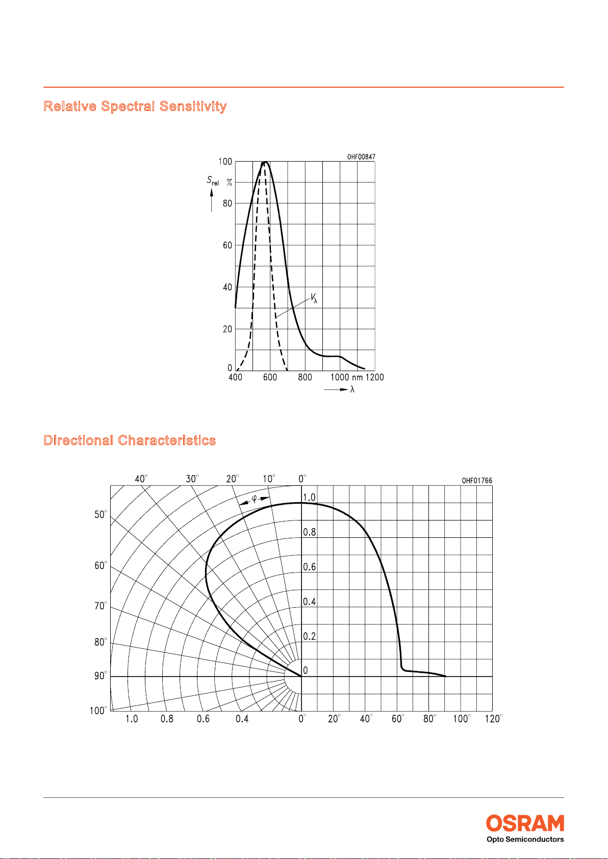
Relative Spectral Sensitivity
S
= f (λ)
rel
1), 2)
Directional Characteristics
S
= f (φ)
rel
1), 2)
Version 1.3 | 2018-06-21
4
Page 5
BPW 21
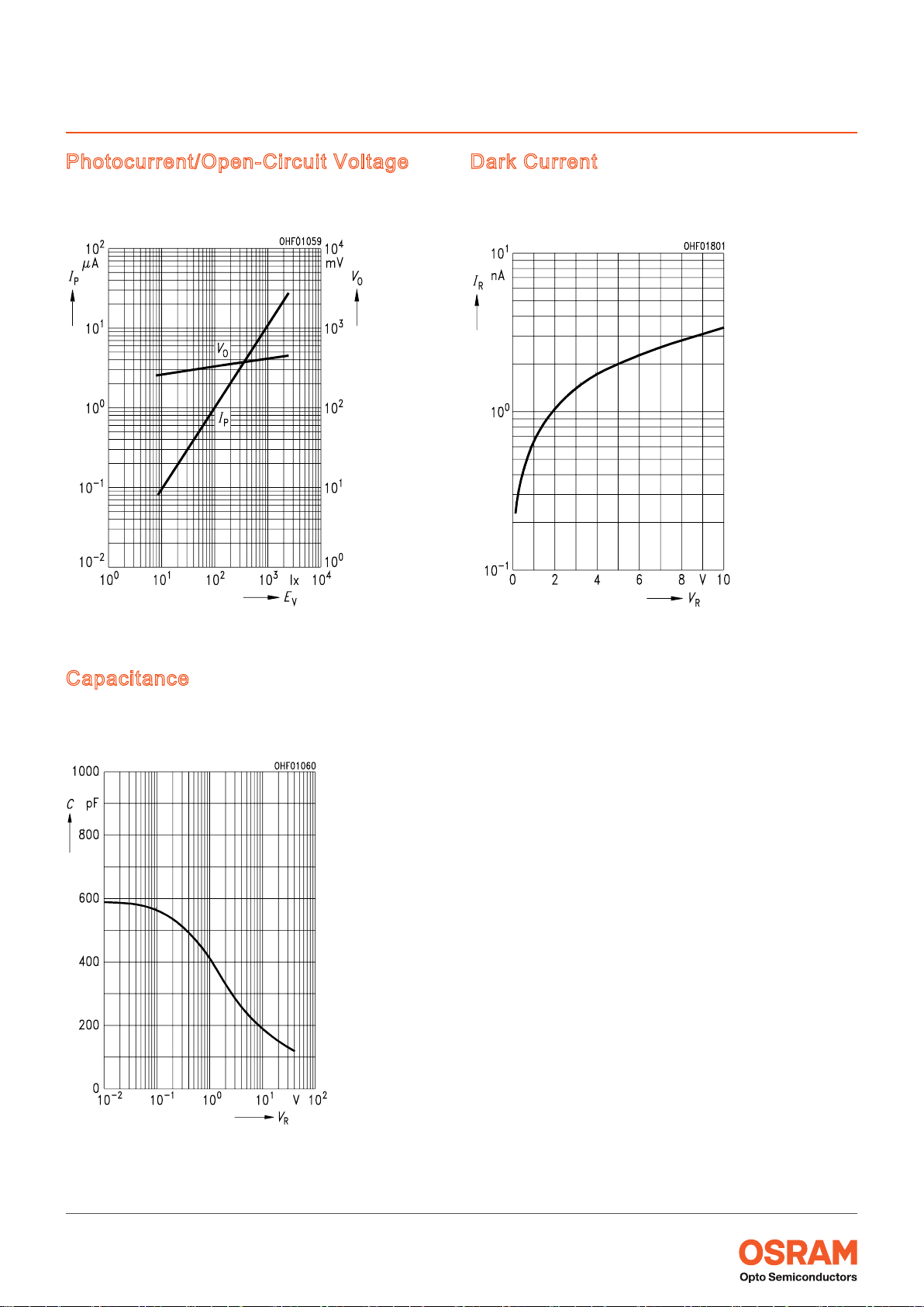
Photocurrent/Open-Circuit Voltage
IP (VR = 5 V) / VO = f (Ev)
1), 2)
Dark Current
IR = f (VR) ; E = 0
1), 2)
Capacitance
C = f (VR); f = 1 MHz; E = 0;
1), 2)
Version 1.3 | 2018-06-21
5
Page 6
BPW 21
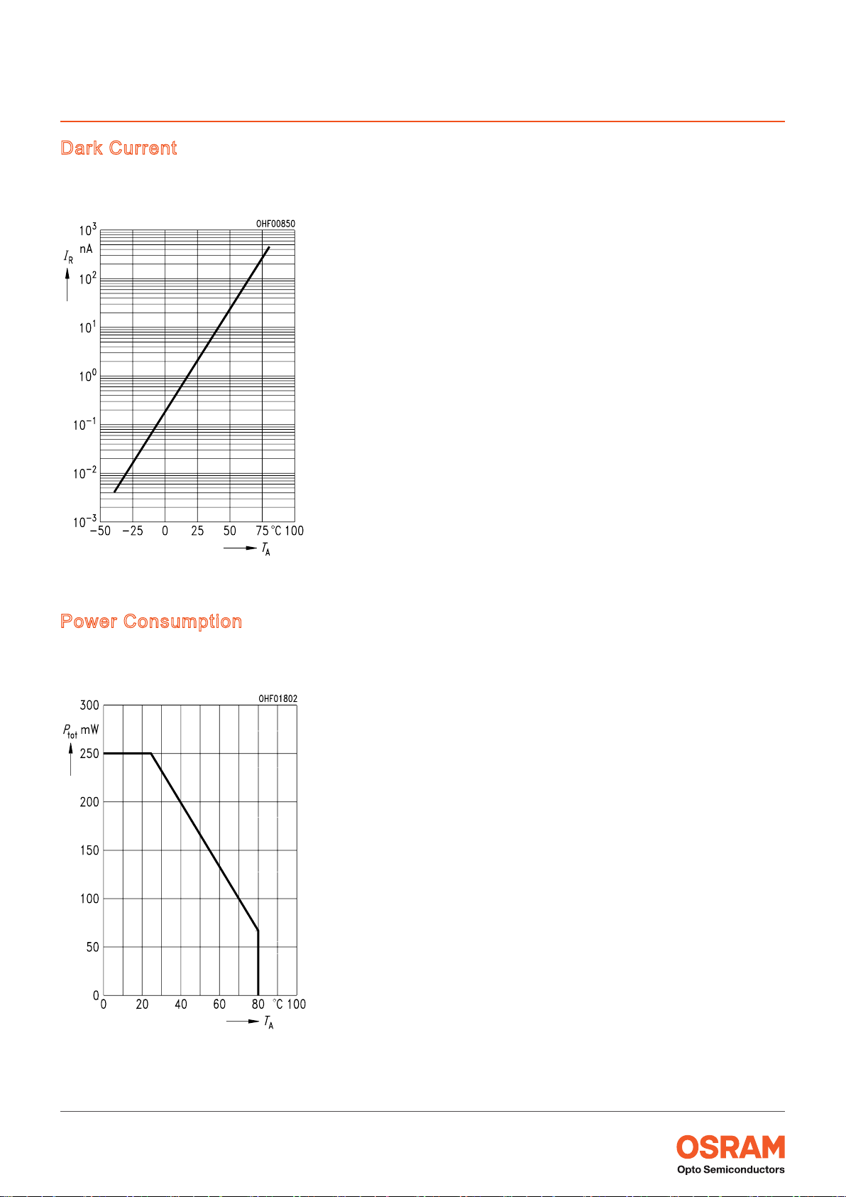
Dark Current
IR = f (TA); E = 0; VR = 5 V
2)
Power Consumption
P
= f (TA);
tot
Version 1.3 | 2018-06-21
6
Page 7
BPW 21
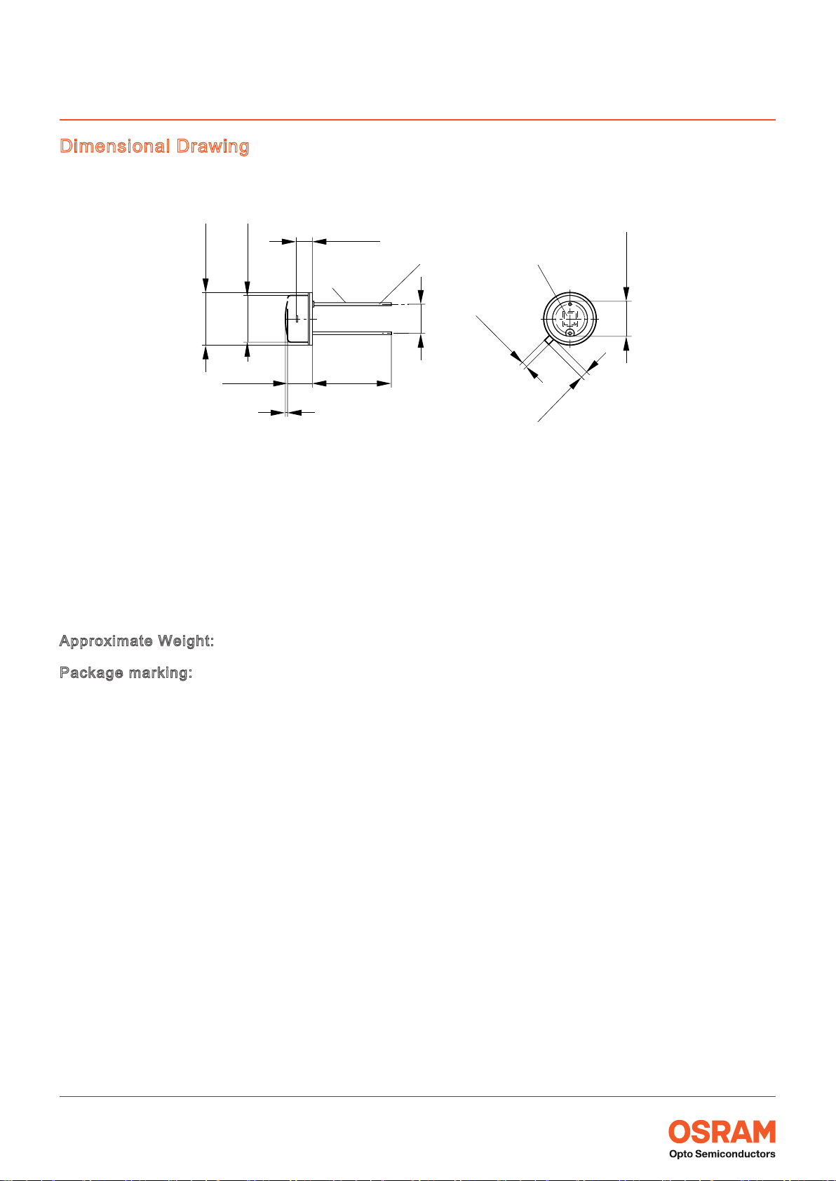
Dimensional Drawing
ø9.5 (0.374)
ø9.0 (0.354)
ø8.3 (0.327)
3.4 (0.134)
3.0 (0.118)
0.3 (0.012) max
Approx. weight 2 g
3)
Chip position
1.75 (0.069)
1.55 (0.061)
ø8.0 (0.315)
ø0.45 (0.018)
14.5 (0.571)
12.5 (0.492)
Cathode
5.08 (0.200)
Radiant
sensitive area
0.85 (0.033)
0.65 (0.026)
spacing
1.0 (0.039)
0.8 (0.031)
ø6.0 (0.236)
ø5.8 (0.228)
GMOY6011
Approximate Weight: 855.0 mg
Package marking:
Cathode
Version 1.3 | 2018-06-21
7
Page 8
BPW 21
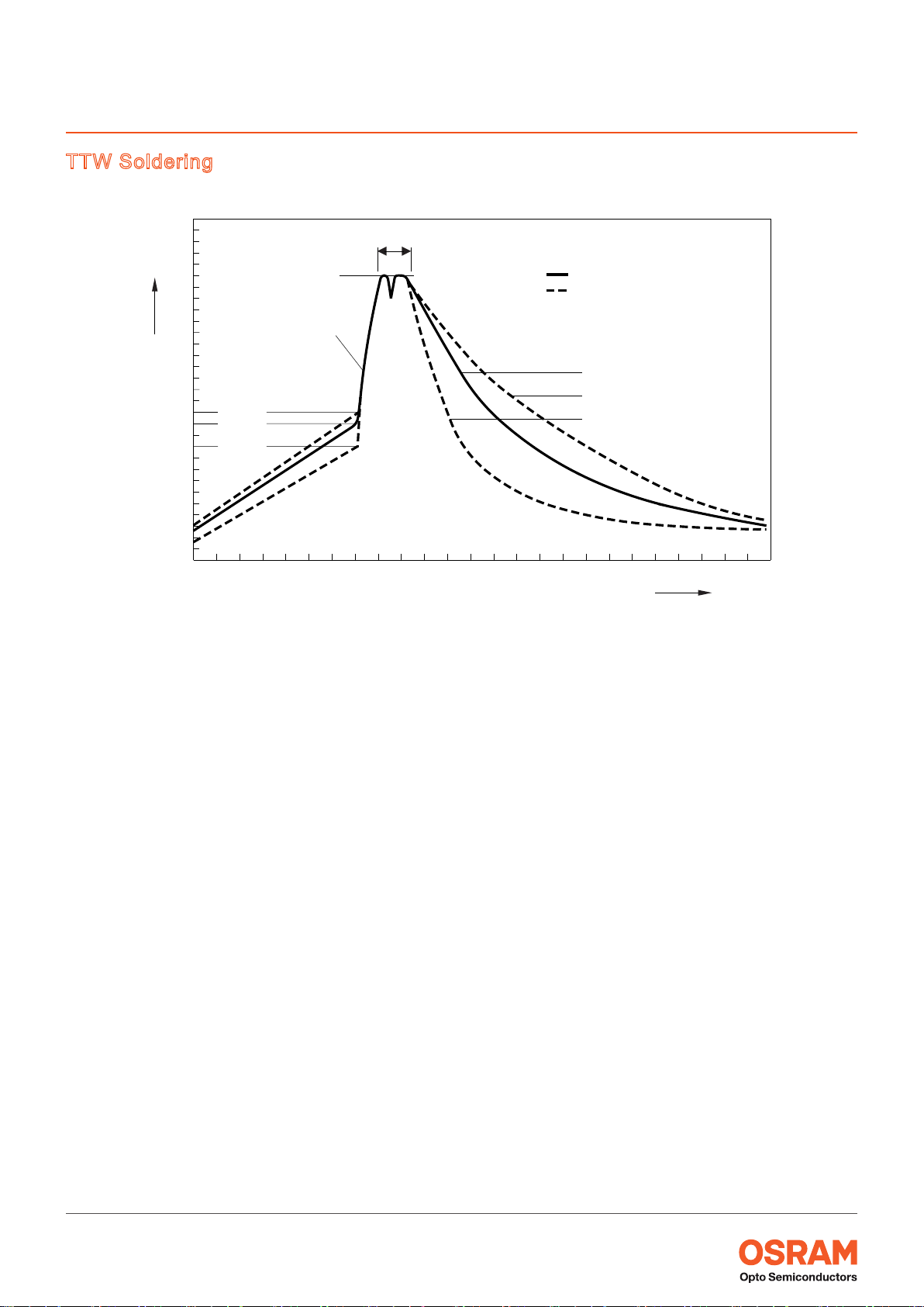
OHA04645
t
TTW Soldering
IEC-61760-1 TTW
300
˚C
T
250
200
150
100
50
10 s max., max. contact time 5 s per wave
235 ˚C - 260 ˚C
Second wave
Preheating
130 ˚C
120 ˚C
100 ˚C
First wave
T
∆
< 150 K
Continuous line: typical process
Dotted line: process limits
Cooling
ca. 3.5 K/s typical
ca. 2 K/s
ca. 5 K/s
Typical
0
0
20 40 60 80 100 120 140 160 180 200 220 240
s
Version 1.3 | 2018-06-21
8
Page 9
BPW 21
Notes
The evaluation of eye safety occurs according to the standard IEC 62471:2006 (photo biological safety of
lamps and lamp systems). Within the risk grouping system of this IEC standard, the LED specied in this
data sheet falls into the class exempt group (exposure time 10000 s)
sure time, conditions of the eye pupils, observation distance), it is assumed that no endangerment to the
eye exists from these devices. As a matter of principle, however, it should be mentioned that intense light
sources have a high secondary exposure potential due to their blinding eect. When looking at bright light
sources (e.g. headlights), temporary reduction in visual acuity and afterimages can occur, leading to irritation, annoyance, visual impairment, and even accidents, depending on the situation.
Subcomponents of this LED contain, in addition to other substances, metal lled materials including silver.
Metal lled materials can be aected by environments that contain traces of aggressive substances. There-
fore, we recommend that customers minimize LED exposure to aggressive substances during storage, production, and use. LEDs that showed visible discoloration when tested using the described tests above did
show no performance deviations within failure limits during the stated test duration. Respective failure limits
are described in the IEC60810.
For further application related informations please visit www.osram-os.com/appnotes
. Under real circumstances (for expo-
Version 1.3 | 2018-06-21
9
Page 10
BPW 21
Disclaimer
Disclaimer
Language english will prevail in case of any discrepancies or deviations between the two language wordings.
Attention please!
The information describes the type of component and shall not be considered as assured characteristics.
Terms of delivery and rights to change design reserved. Due to technical requirements components may
contain dangerous substances.
For information on the types in question please contact our Sales Organization.
If printed or downloaded, please nd the latest version in the OSRAM OS Webside.
Packing
Please use the recycling operators known to you. We can also help you – get in touch with your nearest
sales oce.
By agreement we will take packing material back, if it is sorted. You must bear the costs of transport. For
packing material that is returned to us unsorted or which we are not obliged to accept, we shall have to
invoice you for any costs incurred.
Product safety devices/applications or medical devices/applications
OSRAM OS components are not developed, constructed or tested for the application as safety relevant
component or for the application in medical devices.
In case Buyer – or Customer supplied by Buyer– considers using OSRAM OS components in product safety
devices/applications or medical devices/applications, Buyer and/or Customer has to inform the local sales
partner of OSRAM OS immediately and OSRAM OS and Buyer and /or Customer will analyze and coordi-
nate the customer-specic request between OSRAM OS and Buyer and/or Customer.
Version 1.3 | 2018-06-21
10
Page 11

BPW 21
Glossary
1)
Testing temperature: TA = 25°C
2)
Typical Values: Due to the special conditions of the manufacturing processes of LED, the typical data
or calculated correlations of technical parameters can only reect statistical gures. These do not necessarily correspond to the actual parameters of each single product, which could dier from the typical
data and calculated correlations or the typical characteristic line. If requested, e.g. because of technical
improvements, these typ. data will be changed without any further notice.
3)
Tolerance of Measure: Unless otherwise noted in drawing, tolerances are specied with ±0.1 and
dimensions are specied in mm.
Version 1.3 | 2018-06-21
11
Page 12

BPW 21
Published by OSRAM Opto Semiconductors GmbH
Leibnizstraße 4, D-93055 Regensburg
www.osram-os.com © All Rights Reserved.
Version 1.3 | 2018-06-21
12
 Loading...