

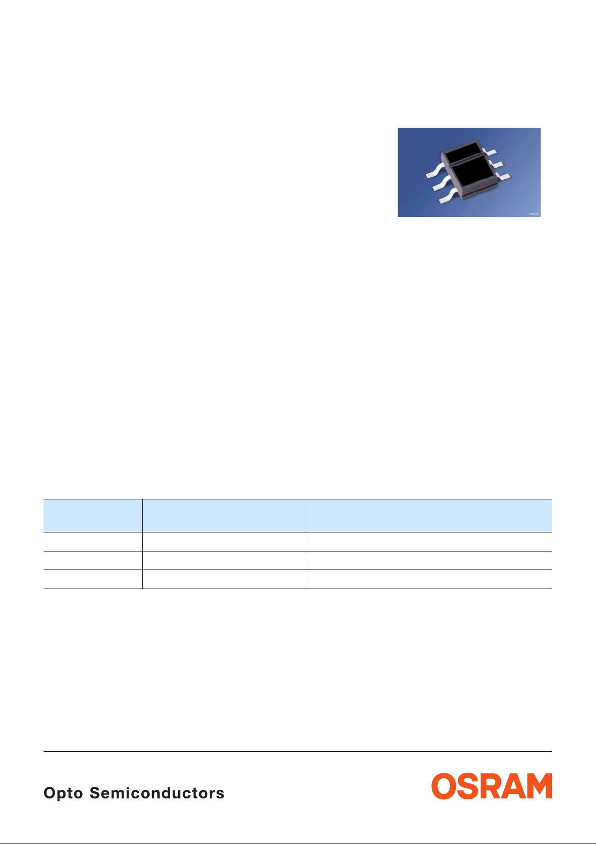
Reflexlichtschranke
Reflective Interrupter
Lead (Pb) Free Product - RoHS Compliant
SFH 9201
Wesentliche Merkmale
• Optimaler Arbeitsabstand 1 mm bis 5 mm
• IR-GaAs-Lumineszenzdiode in Kombination
mit einem Si-NPN-Fototransistor
• Tageslichtsperrfilter
• Geringe Sättigungsspannung
• Sender und Empfänger galvanisch getrennt
• Lötmethode: IR-Reflow Löten
• Vorbehandlung nach JEDEC Level 4
Anwendungen
• Positionsmelder
• Endabschaltung
• Drehzahlüberwachung, -regelung
• Bewegungssensor
Typ
Type
SFH 9201 Q65110A2708 0.25 … 2.00
Bestellnummer
Ordering Code
Features
• Optimal operating distance 1 mm to 5 mm
• IR-GaAs-emitter in combination with a Silicon
NPN phototransistor
• Daylight cut-off filter
• Low saturation voltage
• Emitter and detector electrically isolated
• Soldering Methode: IR Reflow Soldering
• Preconditioning acc. to JEDEC Level 4
Applications
• Position reporting
• End position switch
• Speed monitoring and regulating
• Motion transmitter
I
[mA]
CE
I
= 10 mA, VCE = 5 V, d = 1 mm
F
SFH 9201-2/3 Q65110A2698 0.40 … 1.25
SFH 9201-3/4 Q65110A2716 0.63 … 2.00
2005-07-08 1
Grenzwerte
Maximum Ratings
SFH 9201
Bezeichnung
Parameter
Sender (GaAs-Diode)
Emitter (GaAs diode)
Sperrspannung
Reverse voltage
Vorwärtsgleichstrom
Forward current
Verlustleistung
Power dissipation
Empfänger (Si-Fototransistor)
Detector (silicon phototransistor)
Dauer-Kollektor-Emitter-Sperrspannung
Continuous collector-emitter voltage
Kollektor-Emitter-Sperrspannung, (
Collector-emitter voltage, (
t ≤ 2 min)
t ≤ 2 min)
Symbol
Symbol
V
R
I
F
P
tot
V
CE
V
CE
Wert
Value
Einheit
Unit
5V
50 mA
80 mW
16 V
30
Emitter-Kollektor-Sperrspannung
V
EC
7
Emitter-collector voltage
Kollektorstrom
I
C
20 mA
Collector current
Verlustleistung
P
tot
100 mW
Total power dissipation
Reflexlichtschranke
Light Reflection Switch
Lagertemperatur
T
stg
– 40 … + 100 °C
Storage temperature range
Umgebungstemperatur
T
A
– 40 … + 100
Ambient temperature range
Verlustleistung
P
tot
150 mW
Power dissipation
Elektrostatische Entladung
ESD 2 KV
Electrostatic discharge
Umweltbedingungen / Environment conditions 3 K3 acc. to EN 60721-3-3 (IEC 721-3-3)
2005-07-08 2
Kennwerte (TA = 25 °C)
Characteristics
SFH 9201
Bezeichnung
Parameter
Sender (IR-GaAs-Diode)
Emitter (IR-GaAs diode)
Durchlaβspannung
Forward voltage
I
= 50 mA
F
Sperrstrom
Reverse current
V
= 5 V
R
Kapazität
Capacitance
V
= 0 V, f = 1 MHz
R
Wärmewiderstand
Thermal resistance
1)
1)
Empfänger (Si-Fototransistor)
Detector (silicon phototransistor)
Symbol
Symbol
V
F
I
R
C
O
R
thJA
Wert
Value
Einheit
Unit
1.25 (≤ 1.65) V
0.01 (≤ 1) µA
25 pF
270 K/W
Kapazität
Capacitance
V
= 5 V, f = 1 MHz
CE
Kollektor-Emitter-Reststrom
Collector-emitter leakage current
V
= 20 V
CE
Fotostrom (Fremdlichtempfindlichkeit)
Photocurrent (outside light density)
V
= 5 V, EV = 1000 Lx
CE
Wärmewiderstand
Thermal resistance
1)
1)
C
I
CEO
I
P
R
CE
thJA
10 pF
3 (≤ 200) nA
3.5 mA
270 K/W
2005-07-08 3
Kennwerte (TA = 25 °C)
Characteristics (cont’d)
SFH 9201
Bezeichnung
Parameter
Reflexlichtschranke
Light Reflection Switch
Kollektor-Emitterstrom
Collector-emitter current
Kodak neutral white test card, 90% Reflexion
I
= 10 mA; VCE = 5 V; d = 1 mm
F
Kollektor-Emitter-Sättigungsspannung
Collector-emitter-saturation voltage
Kodak neutral white test card, 90% Reflexion
I
= 10 mA; d = 1 mm; IC = 85 µA
F
1)
Montage auf PC-Board mit > 5 mm2 Padgröβe
1)
Mounting on pcb with > 5 mm2 pad size
d
Symbol
Symbol
I
CE min.
I
CE typ.
V
CE sat
Wert
Value
0.25
0.70
0.15 (≤ 0.6) V
Einheit
Unit
mA
mA
Reflector
with 90% reflexion
(Kodak neutral white
test card)
OHM02257
2005-07-08 4

Schaltzeiten (TA = 25 °C, VCC = 5 V, IC = 1 mA1), RL = 1 kΩ)
Switching Times
R
L
Ι
F
Ι
C
V
CC
Output
OHM02258
SFH 9201
Bezeichnung
Parameter
Einschaltzeit
Turn-on time
Anstiegzeit
Symbol
Symbol
t
ein
t
on
t
r
Wert
Value
Einheit
Unit
65 µs
50 µs
Rise time
Ausschaltzeit
Turn-off time
Abfallzeit
t
t
t
aus
off
f
55 µs
50 µs
Fall time
1)
I
eingestellt über den Durchlaβstrom der Sendediode, den Reflexionsgrad und den Abstand des Reflektors vom
C
Bauteil (
1)
I
C
reflector and component (
d)
as a function of the forward current of the emitting diode, the degree of reflection and the distance between
d)
2005-07-08 5
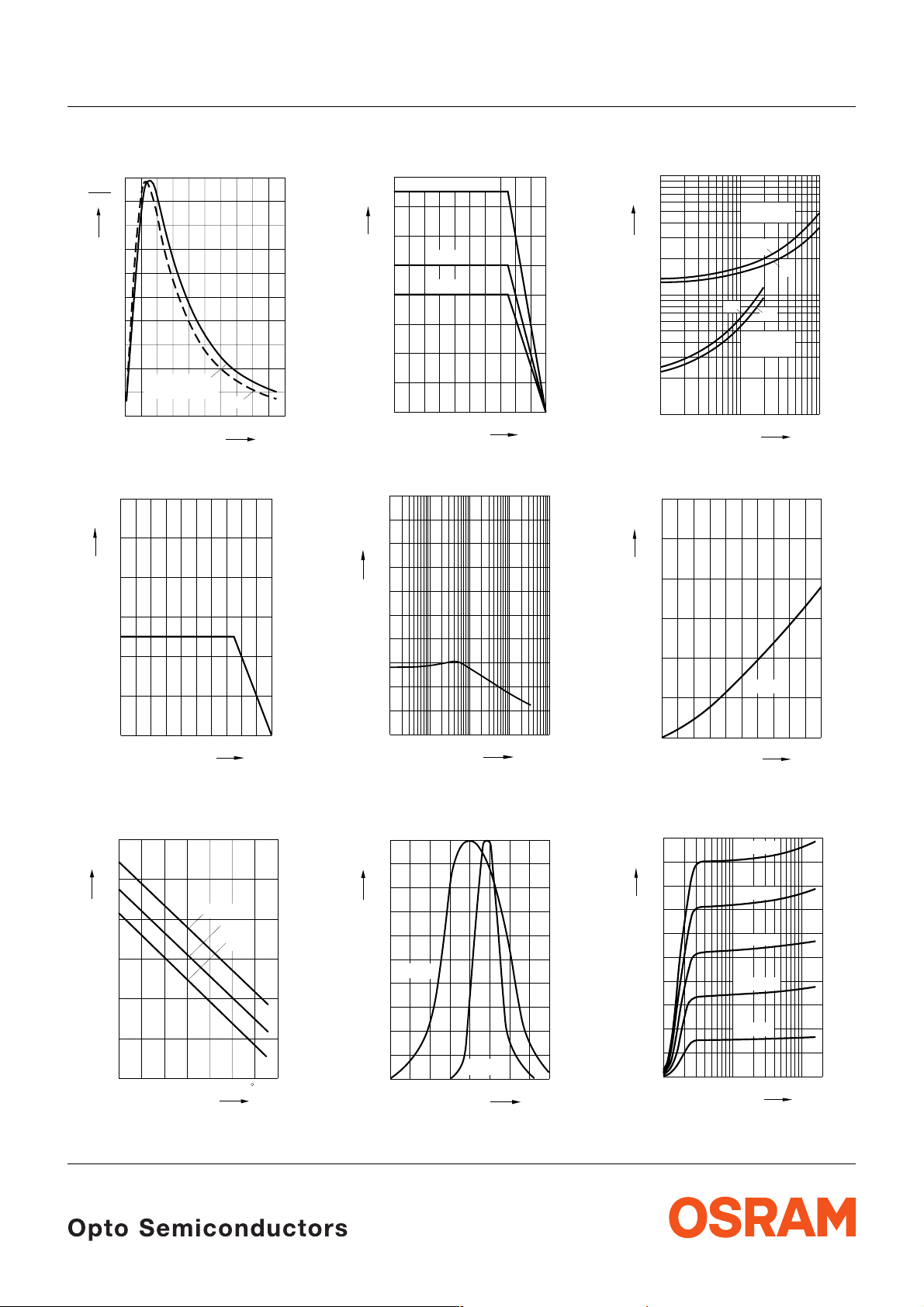
I
Collector Current
100
Ι
C
Ι
%
C
max
80
60
40
20
Kodak neutral
white test card
0
0
1234mm5
C
---------- fd()=
I
Cmax
Mirror
OHO02255
d
Max. Permissible Forward Current
I
= f (TA)
F
120
mA
I
F
100
80
60
40
20
0
020406080˚C
OHL00986
T
A
100
Forward Voltage (typ.) of the
V
Diode
= f (T)
F
Ι
= 20 mA
F
OHO02256
10 mA
5 mA
C
T
1.30
V
V
F
1.25
1.20
1.15
1.10
1.05
1
-40
-20 0 20 40 60 100
Permissible Power Dissipation for
Diode and Transistor
160
Total power dissipation
mW
P
tot
120
100
80
60
40
20
0
Detector
Emitter
020406080˚C
P
= f (TA )
tot
OHL00945
100
T
A
Transistor Capacitance (typ.)
C
= f (VCE), TA = 25 °C, f = 1 MHz
CE
50
pF
C
40
CE
35
30
25
20
15
10
5
0
10
-1
-2
10010110210V
OHO00374
V
CE
Relative Spectral Emission of
Emitter (GaAs) I
Detector (Si)
100
Ι
rel
S
%
rel
80
60
Detector
40
20
0
700
= f (λ) and
rel
S
= f (λ)
rel
800
900 1000 nm 1100
OHO00786
Emitter
λ
SFH 9201
Switching Characteristics t = f (RL)
T
= 25 °C, IF = 10 mA
A
3
10
t
µ
s
2
10
1
10
-1
10
Collector Current
Ι
t
on
Ι
0
10
I
C
d to reflector = 1 mm, 90% reflection
3.0
mA
Ι
C
2.5
2.0
1.5
1.0
0.5
V
0
0
4 8 12 16 20
Output Characteristics (typ.)
I
= f (VCE), spacing to reflector:
C
d = 1 mm, 90% reflection, T
2.0
Ι
mA
C
1.6
1.4
1.2
1.0
0.8
0.6
0.4
0.2
0
0.1
Ι
F
Ι
F
Ι
F
Ι
F
= 5 mA
Ι
F
10 V010
OHO00785
100µA
=
C
t
on
t
off
t
off
= 1 mA
C
1
10
k
Ω
R
L
= f (IF), spacing
OHO00783
=5 V
CE
mA
Ι
F
= 25 °C
A
OHO00781
= 25 mA
= 20 mA
= 15 mA
= 10 mA
1
V
CE
2005-07-08 6

SFH 9201
Perm. Pulse Handling Capability
I
= f (tp), Duty cycle D = parameter,
F
T
= 25 °C
A
4
10
mA
I
F
3
10
0.2
0.5
2
10
=
D
D
0.005
0.01
0.02
0.05
0.1
1
1
10
1010 10
-2-3-4-5
OHF02623
t
P
t
P
T
I
F
T
=
10 s10
t
p
210-1
1010
10
Perm. Pulse Handling Capability
I
= f (tp), Duty cycle D = parameter,
F
T
= 85 °C
A
4
10
mA
I
F
3
10
D
D
0.005
0.01
0.02
0.05
0.1
0.2
2
10
0.5
1
1
10
1010 10
-2-3-4-5
OHF02622
t
P
t
P
=
T
I
F
T
=
10 s10
t
p
210-1
1010
10
2005-07-08 7
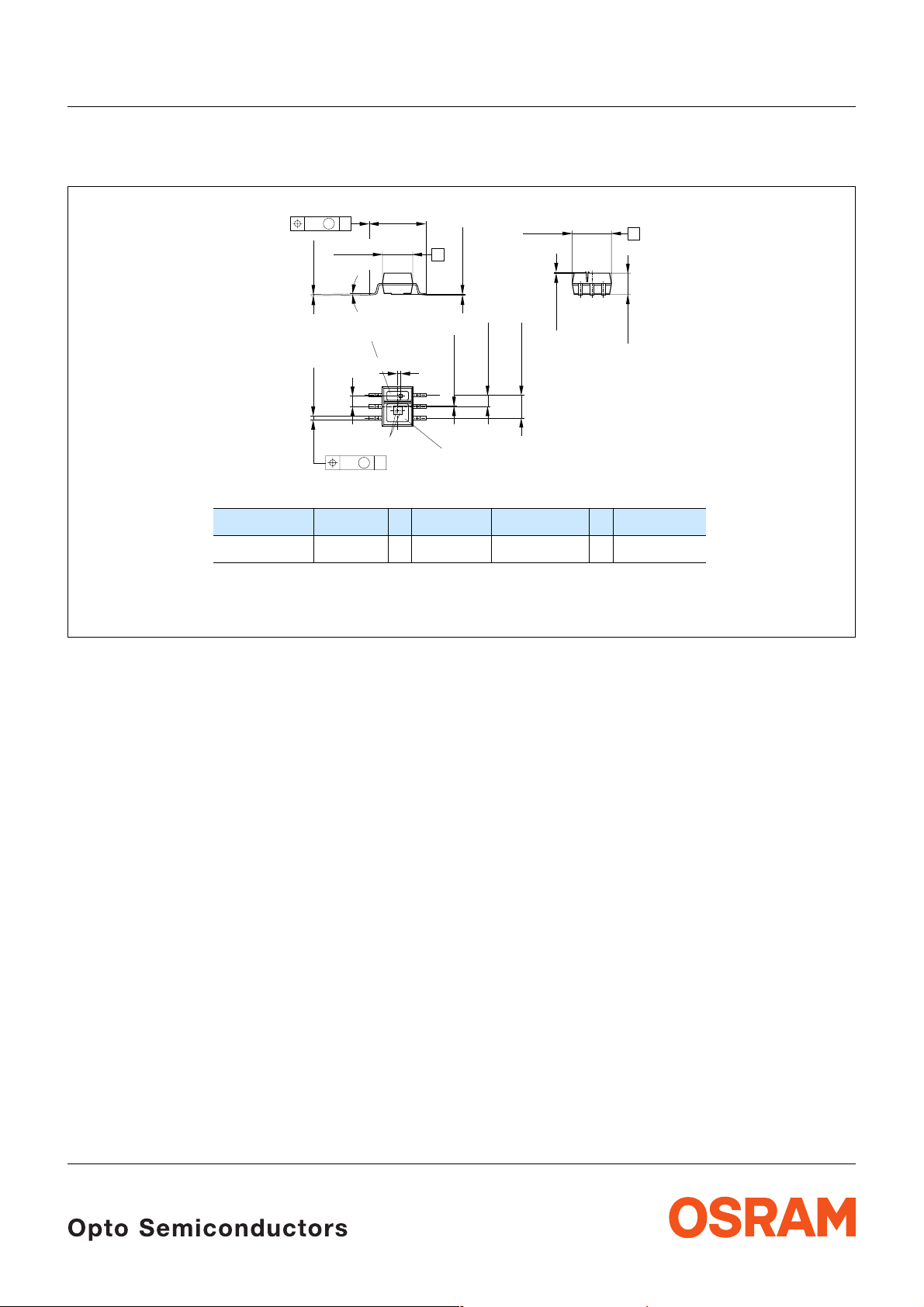
Maßzeichnung
Package Outlines
SFH 9201
M
0.2
0.15 (0.006)
0.13 (0.005)
0.3 (0.012)
0.5 (0.020)
6.2 (0.244)
A
5.8 (0.228)
3.4 (0.134)
3.0 (0.118)
(5˚)
Sender/Emitter
(0.4 (0.016) typ.)
1
25
(1.2 (0.047) typ.)
3
Chip Positionen
M
B
0.1
6
4
Empfänger/Receiver
A
0...0.1 (0...0.004)
Raster (spacing)
1.27 (0.050)
(0.1 (0.004) typ.)
4.2 (0.165)
3.8 (0.150)
(0.05 (0.002) typ.)
Raster (spacing)
2.54 (0.100)
B
2.1 (0.083)
GPLY0504
1.7 (0.067)
Type 1 2 3 4 5 6
SFH 9201 Anode – Emitter Collector – Cathode
Maße werden wie folgt angegeben: mm (inch) / Dimensions are specified as follows: mm (inch).
2005-07-08 8

Empfohlenes Lötpaddesign IR-Reflow Löten
Recommended Solder Pad IR REflow Soldering
0.6 (0.024)
1.27 (0.050)
1.27 (0.050)
Padgeometrie
für verbesserte
Wärmeableitung
SFH 9201
1.2 (0.047)
Paddesign
for improved
Heat dissipation
Cu-Fläche >5 mm
Cu-area >5 mm
2
2
3.9 (0.154)
Lötstopplack
Solder resist
Maße werden wie folgt angegeben: mm (inch) / Dimensions are specified as follows: mm (inch).
OHPY0030
2005-07-08 9
Löthinweise
Soldering Conditions
SFH 9201
Bauform
Type
Drypack
Level acc.
to
IPS-stand.
020
Tauch-, Schwalllötung
Dip, Wave Soldering
Peak Temp.
(solderbath)
Max. Time in
Peak Zone
Reflowlötung
Reflow Soldering
Peak Temp.
(package
temp.)
Max. Time
in Peak
Zone
Kolbenlötung
Iron Soldering
(Iron temp.)
SFH 9201 4 n. a. – 260 °C 20 sec. n.a.
Bitte Verarbeitungshinweise für SMT-Bauelemente beachten!
Please observe the handling guidelines for SMT devices!
Lötbedingungen Vorbehandlung nach JEDEC Level 4
Soldering Conditions Preconditioning acc. to JEDEC Level 4
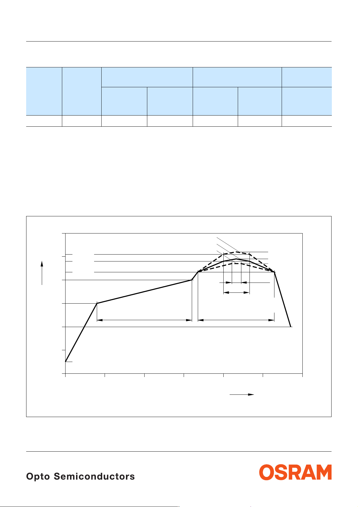
IR-Reflow Lötprofil für bleifreies Löten (nach J-STD-020B)
IR Reflow Soldering Profile for lead free soldering (acc. to J-STD-020B)
I
300
˚C
250
T
200
255 ˚C
240 ˚C
217 ˚C
Maximum Solder Profile
Recommended Solder Profile
Minimum Solder Profile
10 s min
30 s max
OHLA0687
260 ˚C
245 ˚C
235 ˚C
+0 ˚C
-5 ˚C
±5 ˚C
+5 ˚C
-0 ˚C
150
120 s max
100
Ramp Up
25 ˚C
0
3 K/s (max)
50 100 150 200 250 300
50
0
2005-07-08 10
Ramp Down
6 K/s (max)
100 s max
s
t

SFH 9201
Gurtung / Polarität und Lage siehe Dokument: Short Form Katalog: Gurtung und
Verpackung - SMT-Bauelemente - Gehäuse:SMT RLS
Methode of Taping / Polarity and Orientation see document: Short Form Catalog: Tape and Reel -
SMT-Components - Package: SMT-RLS
Published by
OSRAM Opto Semiconductors GmbH
Wernerwerkstrasse 2, D-93049 Regensburg
www.osram-os.com
© All Rights Reserved.
The information describes the type of component and shall not be considered as assured chara cteristics.
Terms of delivery and rights to change design reserved. Due to technical requirements components may contain
dangerous substances. For information on the types in question please contact our Sales Organization.
Packing
Please use the recycling operators known to you. We can also help you – get in touch with your nearest sales office.
By agreement we will take packing material back, if it is sorted. You must bear the costs of transport. For packing
material that is returned to us unsorted or wh ich we are not obliged to accept, we shall hav e to invoice you for any costs
incurred.
Components used in life-support devices or systems must be expressly authorized for such purpose! Critical
components
1
A critical component is a component used in a life-support device or sys tem whose failure can reasonably be expected
to cause the failure of that life-support device or system, or to affec t its safety or e ffectiveness of that dev ice or system.
2
Life support devices or systems are intended (a) to be implanted in the human body , or (b) to support and/or maintain
and sustain human life. If they fail, it is reasonable to assume that the health of the user may be endangered.
2005-07-08 11
1
, may only be used in life-support devices or systems 2 with the express written approval of OSRAM OS.
 Loading...