

Reflexlichtschranke
Reflective Optical Switch
Lead (Pb) Free Product - RoHS Compliant
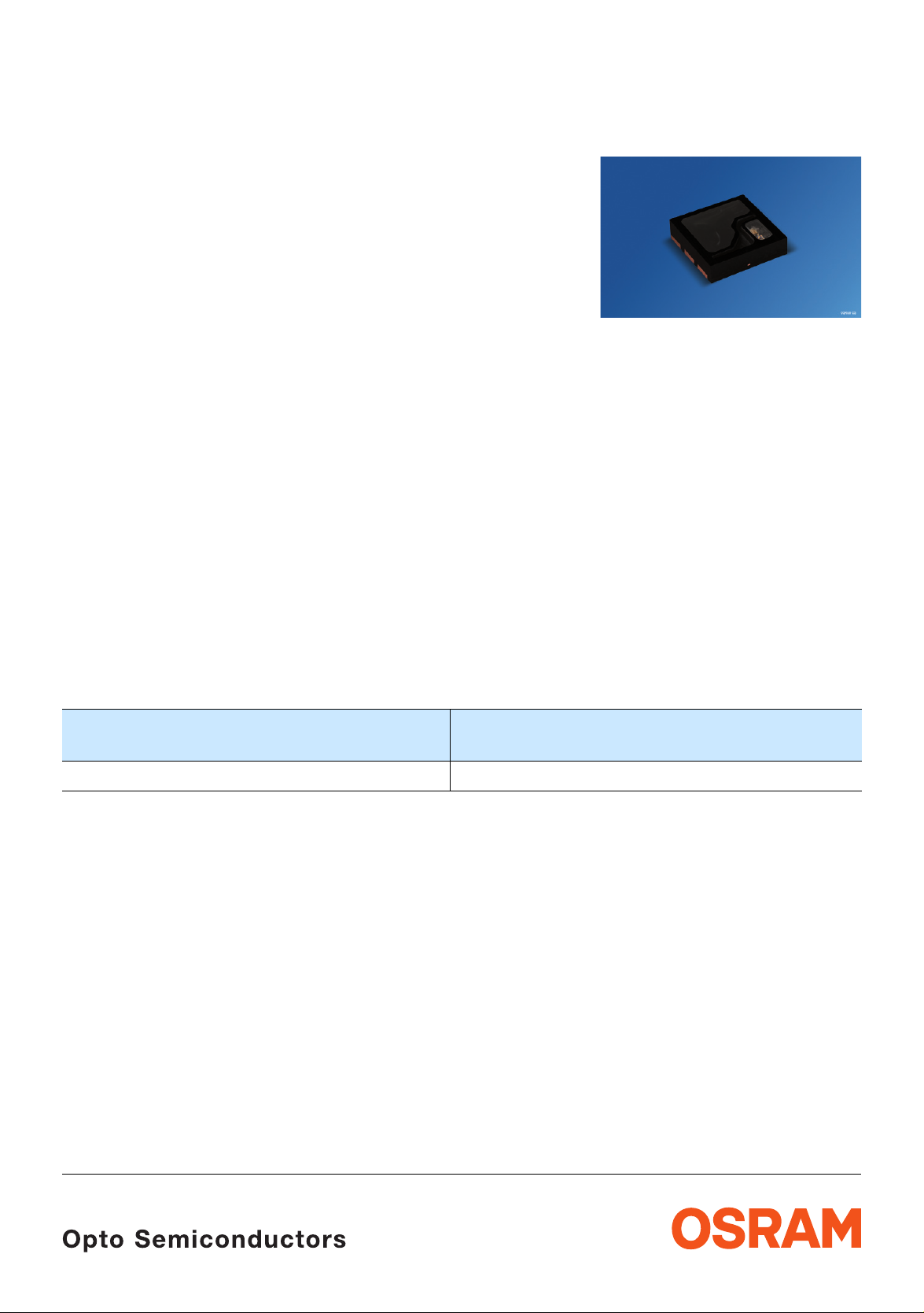
SFH 7740
Wesentliche Merkmale
• Arbeitsabstand: 0.5 - 4 mm
• Arbeitsbereich einstellbar
• Optohybrid mit Schmitt-Trigger Ausgang, open
drain
• Extrem niedriger Stromverbrauch
• Sehr kleines SMD Gehäuse
• Hohe Umgebungslicht Unterdrückung
Anwendungen
• Positionserkennung von Abdeckungen für
Batteriefächer, Foto-Objektiven usw.
• Mobile Geräte
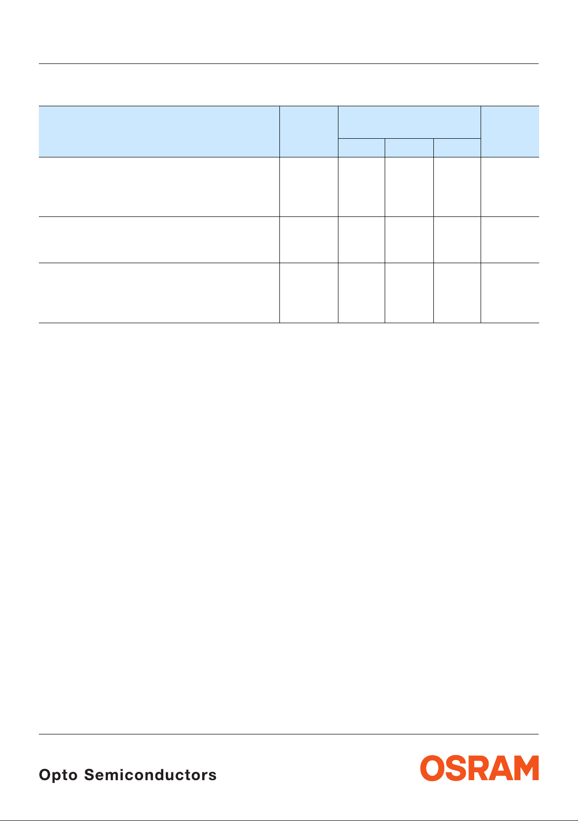
Typ
Type
SFH 7740 Q65110A6668
Features
• Working distance: 0.5 - 4 mm
• Working range adjustable
• Opto hybrid with Schmitt trigger output, open
drain
• Extremly low power consumptio n
• Very small SMD package
• High ambient light suppression
Applications
• Position detection of sliding covers for
battery-cases, camera lenses ect.
• Mobile devices
Bestellnummer
Ordering Code
An application note is available for this product.
Please contact your appropriate OSRAM sales partner
2009-01-14 1
Grenzwerte Maximum Ratings
SFH 7740
Bezeichnung
Parameter
Lagertemperatur
Storage temperature
Versorgungsspannung
Supply voltage
Externe Spannung an Pin
External voltage at pin
Out
Prog
Test
Anode LED
Sink current durch Ausgangstransistor
Sink current through output transistor
(please see figure 1)
Vorwärtsstrom
1)
Forward current
(please see figure 1)
Elektrostatische Entladung
Electrostatic discharge
- Human Body Model
(according to: JESD22-A114E; Class2)
- Machine Model
(according to: JESD22-A115A; Class B)
Symbol
Symbol
T
stg
V
dd
V
out
I
sink
I
f
ESD
Wert
Value
min: – 40
Einheit
Unit
°C
max: + 85
0 - 6 V
V
0 - 4.5
0 - 4.5
0 - 4.5
0 - 1.5
10 mA
60 mA
2
200
kV
V
latch up protection
latch up protection
(according to: EIA/JESD78 Class 1)
1)
Der Vorwärtsstrom If durch die LED ist abhängig von Vdd und R
* The forward current If depends on Vdd and R
2009-01-14 2
as in the following formula:
prog
wie folgt:
prog
20 mA
V
6×
dd
⎛⎞
------------------
If10mA
+=
⎝⎠
R
prog
Empfohlene Betriebsbedingungen
Recommended Operating Conditions
SFH 7740
Bezeichnung
Parameter
Betriebstemperatur
Operating temperature
Versorgungsspannung
Supply voltage
Ausgangsspannung
Output voltage
(please see figure 1)
Rauschen der Versorgungsspannung
Supply voltage ripple
frequency range 0...20kHz
Pull-up Widerstand
Pull-up resistor
(please see figure 1)
Abblock Kondensatoren
Bypass capacitors
(please see figure 1)
Symbol
Symbol
Wert
Value
Einheit
Unit
min. typ. max.
T
op
V
dd
DV
dd
1)
dV
dd
R
pull-up
C
bypass
- stabilisation
- HF
– 20 + 85 °C
2.4 3.6 V
1.7 3.6 V
200 mV
10 1000 kΩ
>1
10 - 100
µF
nF
Umgebungslicht
Ambient light
Normlicht / Standard light A
1)
Der Emitter wird mit 10mA bis 60mA gepulst betrieben; das bedeutet, dass jeder Widerstand in Serie zu V
der Versorgungsleitung verursacht. Es wird empfohlen, diesen Serienwiderstand so klein zu halten, dass m ax dV
wird. Beim Betrieb des SFH 7740 im Labor ist vom Einsatz geregelter Spannungsversorgungen abzusehen. Durch das Einschalten der
IRED wird die Quelle kurzzeitig belastet. Diese Belastung kann zu Spannungsschwankungen der Quelle führen, die wiederum die
Funktion des SFH 7740 beeinträchtigen können. Im Normalbetrieb (Akku, Batterie, stabilisierte Netzteile) tritt dieser Effekt nicht auf.
* The emitter is driven with 10 mA to 60 mA in pulsed mode; this means, that any series resistance on the Vdd line causes a voltage drop
at the power pin. It is recommended to keep the series resistance low, so that max dV
sensor in the lab, please do not use regulated voltage supplies. The IR emitter pulse is a high, short load for the power supply. This
load can influence the stability of the output voltage; this instability will influence the operation of the SFH 7740. This effect does not
occur during normal operation of the sensor with batteries, storage batteries, or stabilized voltage supplies.
E
V
Vdd < 3V
Vdd > 3V
2000
4000
einen Spannungsabfall in
dd
is not exceeded. When testing the SFH 7740
dd
lux
nicht überschritten
dd
2009-01-14 3
Kennwerte (Ta = 25°C)
Characteristics
SFH 7740
Bezeichnung
Parameter
Minimale Betriebsspannung für Startphase
Minimum required supply voltage for start-up
(please see figure 2)
Länge der Startphase
Start up time
(please see figure 2)
Mess-Wiederholzeit
Measurement refresh time
(please see figure 2)
LED „An“ Zeit
LED „ON“ Time
(please see figure 3)
Mittlere Stromaufnahme
Mean current consumption
R
= h, Vdd = 3V
Prog
1)
1)
Maximale Stromaufnahme
Maximum current consumption
R
= h, Vdd = 3V
Prog
Mittlere Stromaufnahme
Mean current consumption
R
= 470 Ω, Vdd = 3V
Prog
1)
1)
Maximale Stromaufnahme
Maximum current consumption
R
= 470 Ω, Vdd = 3V
Prog
Ausgangsleckstrom „high“
Output leakage current „high“
DVdd = 2.2V
Symbol
Symbol
V
dd, start
t
start
t
refresh
t
pulse
I
dd, mean
I
dd, max
I
dd, mean
I
dd, max
I
out, H
Wert
Value
Einheit
Unit
min. typ. max.
0.8 2.0 V
60 90 120 ms
60 90 120 ms
30 45 60 µs
25 50 μA
10 20 mA
45 75 μA
50 65 mA
5 400 nA
Ausgangsspannung „low“
V
Output voltage „low“
DVdd = 2.2V; R
Wellenlänge der max. Fotoempfindlichkeit
pullup
= 270 Ω
λ
Wavelength of max. sensitivity
2009-01-14 4
out, L
S, max
0.1 0.5 V
880 nm
Kennwerte (Ta = 25°C)
Characteristics
SFH 7740
Bezeichnung
Parameter
Spektraler Bereich der Fotoempfindlichkeit
S = 10% von S
max
Symbol
Symbol
λ 730 1080 nm
Spectral range of sensitivity
S = 10% of S
Wellenlänge der Strahlung des Emitters
max
λ
peak
Wavelength at peak emission
I
= 10 mA
F
Spektrale Bandbreite des Emitters bei 50% von
I
max
Spectral bandwidth of the emitter at 50% of I
Δλ 30 nm
max
IF = 10 mA
1)
gepulster Betrieb: Dauer LED an: ~44µs / Dauer LED aus: ~90ms
* pulsed operating mode: LED on time: ~44µs / LED off time: ~90ms
Wert
Value
min. typ. max.
850 nm
Einheit
Unit
2009-01-14 5

Schaltabstand und Reflektoreigenschaften
Switching distance and reflector characteristics
SFH 7740
Bezeichnung
Parameter
Symbol
Symbol
min. typ. max.
Reflektor Reflektivität
R
R 850nm
50 %
Reflector reflectivity
λ = 850nm
Absorber Reflektivität
R
A 850nm
Absorber reflectivity
λ = 850nm
Kontrast Verhältnis (Reflektor / Absorber)
contrast ratio (Reflector / absorber)
Reflektor und Absorber Größe
Reflector and absorber size
Einstellbarer Arbeitsabstand
Adjustiable working distance
Variation des Arbeitsabstandes
Variation of working distance
1)
siehe / see Application note: „Reflective Optical Sensor SFH 7740“.
2)
Der Abeitsabstand d ist definiert von der Sensoroberfläche bis zum Reflektor. d
Reflektor (Reflektionsgrad R>60%) und Absorber (R<6%) erreicht werden.
* The working distance d is defined from to p of the sensor to reflecto r surface. d
a reflector (reflection coefficient R>60%) and absorber ( R<6%).
1)
1)
(w x l)
2)
2)
1)
1)
(B x L)
R
R 850nm
R
A 850nm
A
reflector
A
absorber
d 0.5 4 mm
Δ
d +/- 0.4 mm
/
10
min
Wert
Value
und d
min
and d
Einheit
Unit
9 %
können nur mit einem
max
can only be reached with
max
Graph 1: Adjustion of different working distances by emitter current If and R
60
50% 60%
50
40
If / mA
30
20
10
0.5 1 1.5 2 2.5 3 3.5 4
2009-01-14 6
d / mm
70%
80%
90%
R
prog as func
prog
V
-------------------------=
I
f
dd
10mA–
6×

Blockdiagramm (empfohlener Pull-Up-Widerstand Rpull up = 10kOhm...100kOhm)
Block diagram (recommended Pull up resistance Rpull up = 10kOhm...100kOhm)
Figure 1 Blockdiagramm
Block diagram
C
HF
R
Prog
SFH 7740
LED Anode
(must not be
connected)
Prog
LED
I
F
C
stabilisation
ASIC
GNDGND
V
dd
Phototransistor
I
sink
GND
Test
GND
DV
Out
Device
boundaries
dd
R
pull up
OHF03409
V
Out
2009-01-14 7

Figure 2 Startverhalten
Start-up sequence
V
dd
V
dd_start max
V
dd_start min
Out
High
Low
t
1
Default
Low
120 ms +
60 ms -
t
1
SFH 7740
t
For reflector
For absorber
or no reflector
t
t
1
Undefined high or low output impedance
Der Ausgang ist immer hochohmig, wenn an Vdd keine Spannung angeschlossen ist. Wenn die
Versorgungsspannung V
findet etwa alle 90ms eine Messung des reflektierten Signals statt und der Ausgang wird entprechend
geschalten (Figure 3).
If the supply voltage at V
V
signal is measured and the output is set accordingly (Figure 3).
, the sensor output stays low for 60ms < t
dd, start
erreicht, bleibt der Ausgang für 60ms < t
dd, start
is not connected, the output is always high ohmic. When supply voltage reaches
dd
<120ms. Subsequently approx. every 90ms the reflected
start
start
OHF03836
<120ms auf „low“. Anschließend
Figure 3 Timing diagram
Ι
f
t
Out
High
Low
t
pulse
t
refresh
For reflector
For absorber
or no reflector
t
OHF03835
2009-01-14 8

SFH 7740
LED:
Relative Spectral Emission
I
= f (λ); TA = 25°C
rel
100
%
I
rel
80
60
40
20
0
700
OHL01714
nm
λ
Phototransistor
Relative Spectral Sensitivity
S
= f (λ); TA = 25°C
rel
100
%
Srel
80
60
40
20
950750 800 850
0
700 800 900 1000 1100
lamb d a / n m
SFH 7740:
Mean current consumption
I
= f (Vdd); R
dd
µA
50
I
dd
330Ω
40
30
20
2.4 2.7 3.0 3.3 3.6
; TA = 25°C
prog
/ V
V
dd
470Ω
2kΩ
inf.
2009-01-14 9

Maßzeichnung Package Outlines
SFH 7740
Maße in mm (inch) / Dimensions in mm (inch)
2009-01-14 10

Anschlußbelegung Pin configuration
Pin # Description
1 Anode LED (must not be connected)
2 GND
3 Out
4 Test (must be connected to GND)
SFH 7740
5 V
6 Prog
Bauteilaufnahme device pickup
Vakuum Pipette sollte das Bauteil am rechteckigen Außenrahmen fassen.
Laminar vacuum pickup nozzle should use the rectangular outer wall of the device for handling.
Empfohlenes Pickup Nadel Recommended pickup nozzle
dd
3.6 (0.142)
3.8 (0.150)
13 (0.512)
Maße in mm/ Dimensions in mm
2009-01-14 11
ø1.5 (0.059)
GPLY7058

Empfohlenes Lötpaddesign Recommended Solderpad Design
Maße in mm / Dimensions in mm
Gurtverpackung Taping
SFH 7740
2009-01-14 12

SFH 7740
Maße in mm / Dimensions in mm
2009-01-14 13

SFH 7740
Lötbedingungen Vorbehandlung nach JEDEC Level 4 Soldering Conditions Preconditioning acc. to JEDEC Level 4
Reflow Lötprofil für bleifreies Löten (nach J-STD-020C)
Reflow Soldering Profile for lead free soldering (acc. to J-STD-020C)
300
˚C
250
T
255 ˚C
240 ˚C
Maximum Solder Profile
Recommended Solder Profile
Minimum Solder Profile
217 ˚C
200
10 s min
OHLA0687
260 ˚C
245 ˚C
235 ˚C
+0 ˚C
-5 ˚C
±5 ˚C
+5 ˚C
-0 ˚C
30 s max
150
120 s max
100 s max
Ramp Down
6 K/s (max)
100
Ramp Up
50
3 K/s (max)
25 ˚C
0
0
50 100 150 200 250 300
s
t
Published by
OSRAM Opto Semiconductors GmbH
Wernerwerkstrasse 2, D-93049 Regensburg
www.osram-os.com
© All Rights Reserved.
The information describes the type of component and shall not be considered as assured characteristics. Due to the
special conditions of the manufacturing processes of Sensor, the typical data or calculated correlations of technical
parameters can only reflect statistical figures. These do not necessarily correspond to the actual parameters of each
single product, which could differ from the typical data and calculated correlations or the typical characteristic line. If
requested, e.g. because of technical improvements, these typ. data will be changed without any further notice.
Terms of delivery and rights to change design reserved. Due to technical requirements components may contain
dangerous substances. For information on the types in question please contact our Sales Organization.
Packing
Please use the recycling operators known to you. We can also help you – get in touch with your nearest sales office.
By agreement we will take packing material back, if it is sorted. You must bear the costs of transport. For packing
material that is returned to us unsorted or wh ich we are not obliged to accept, we shall hav e to invoice you for any costs
incurred.
Components used in life-support devices or systems must be expressly authorized for such purpose! Critical
components
1
A critical component is a component used in a life-support device or sys tem whose failure can reasonably be expected
to cause the failure of that life-support device or system, or to affec t its safety or e ffectiveness of that dev ice or system.
2
Life support devices or systems are intended (a) to be implanted in the h uman body, or (b) to support and/or maintain
and sustain human life. If they fail, it is reasonable to assume that the health of the user may be endangered.
2009-01-14 14
1
, may only be used in life-support devices or systems 2 with the express written approval of OSRAM OS.
 Loading...