

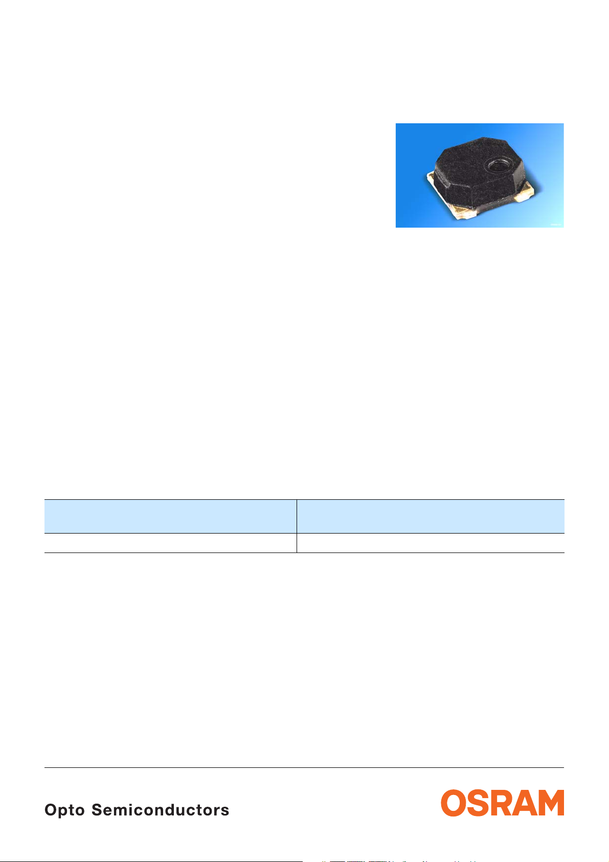
SMD Kippsensor mit digitalem Ausgang (SFH 7710)
SMD Orientation-Sensor with digital output (SFH 7710)
Lead (Pb) Free Product - RoHS Compliant
SFH 7710
Wesentliche Merkmale
• optische Erkennung der Verkippung durch
gravitationsabhängige Position einer
Stahlkugel
• Niedriger Stromverbrauch
• digitaler Ausgang, open drain
• definierter Schaltwinkelbereich
• sehr kleines SMD Gehäuse
• IC gesteuerter Sensor
Anwendungen
• Digitalkameras
•Camcorder
• Mobiltelefone
• Computer Zubehör
Typ
Type
SFH 7710 Q65110A4407
Features
• optical detection of orientationby gravity
dependent position of a steel ball
• Low current consumption
• digital output, open drain
• defined range of switching angle
• very small SMD package
• IC controlled sensor
Applications
• Digital cameras
• Camcorders
• Mobile phones
• Computer peripherals
Bestellnummer
Ordering Code
2007-10-16 1
Grenzwerte
Maximum Ratings
SFH 7710
Bezeichnung
Parameter
Versorgungsspannung
Supply voltage
Ausgangsspannung
Output voltage
Ausgangsstrom
Output current
Lagertemperatur
Storage temperature range
Elektrostatische Entladung
Electrostatic discharge
- human body model (according to: Class I)
- machine model (according to:
AEC-Q100-003-REV-D, classification M3)
latch up Schutz
latch-up protection
(according to: EIA/JESD78 Class I)
Symbol
Symbol
V
cc
V
o
I
10 mA
o
T
-40...100 °C
s
V
ESD
Wert
Value
-0.2...6 V
-0.3...4.5 V
2
200
20 mA
Einheit
Unit
kV
V
2007-10-16 2

Empfohlener Arbeitsbereich
Recommended Operating conditions
SFH 7710
Bezeichnung
Parameter
Symbol
Symbol
Wert
Value
Einheit
Unit
Min Max
Betriebstemperatur
Τ
A
-20 +65 °C
Full operational ambient temperature range
Versorgungsspannung
V
cc
2.3 3.6 V
Supply voltage
Versorgungsspannungsstörungen *
dV
cc pp
0.2 V
(Frequenzbereich: 0...20kHz)
Supply voltage noise
(frequency range: 0...20kHz)
Ausgangsspannung
V
o
1.7 3.6 V
Output voltage
Pull-up Widerstand
R
pull up
10 100 kOhm
Pull-up resistance
* Der Emitter wird mit 10mA gepulst betrieben; das bedeutet, dass jeder Widerstand in Serie zu V
cc
einen Spannungsabfall in der Versorgungsleitung verursacht. Daher wird empfohlen, diesen
V
Serienwiderstand kleiner 10 Ohm zu halten. Die minimale Versorgungsspanung (
) darf keinesfalls
cc min
unterschritten werden.
V
* The emitter is driven with 10 mA in pulsed mode; this means that any series resistor to
causes a
cc
voltage drop on the power line. It is recommended to keep the series resistor below 10 Ohm. The supply
voltage may not fall below
V
cc min
2007-10-16 3

Kennwerte
Characteristics
(TA=25°C)
SFH 7710
Bezeichnung
Parameter
Minimale Betriebsspannung für Startphase(
siehe Figure 3)
Minimum required supply bvoltage for start-up (
Länge der Startphase
Start up time
(see Figure 3
Durchschnittlicher Stromaufnahme
mean current consumption
Spitzenstromaufnahme
peak current consumption
(siehe Figure 3)
)
1)
1)
2)
1)
Ausgangsleckstrom „high“
Output leakage current „high“
O = 3,6V
V
Ausgangsleckstrom „low“
Output leakage current „low“
Ol = 10mA (V
I
Aktualisierung des Ausgangssignals
Refresh of output signal
= 2,3V)
cc
1)
1)
see Figure 3)
Symbol
Symbol
Wert
Value
Einheit
Unit
Min. Typ. Max.
V
cc,start
t
start 60 120 ms
mean
I
0.8 2.0 V
50 µA
Ipeak 20 mA
OH 5µA
I
V
OL 0.5 V
trefresh 90 ms
Kippwinkel mit Ausgangszustand „low“
Tilt angle with output state „low“
(see Figure 1)
Kippwinkel mit Ausgangszustand „high“
Tilt angle with output state „high“
1)
gepulster Betrieb: Dauer LED an: ~44µs / Dauer LED aus: ~90ms
pulsed operation mode: LED on time: ~44µs / LED off time: ~90ms
2)
gepulster Betrieb: Dauer LED an: ~44µs / Dauer LED aus: ~90ms
pulsed operation mode: LED on time: ~44µs / LED off time: ~90ms
2007-10-16 4
(siehe Figure1)
(siehe Figure1)
(see Figure 1)
α
t 70 200 °
α
u 250 20 °

Funktionsdiagramm
Functional diagram
y
V
SFH 7710
αβ
y
20˚
out
= high
Switching Range
70˚
y
60˚-60˚
x
α
z
β
250˚
Switching Range
200˚
Figure1:
Erfassungscharakteristik / Detecting characteristics
(Unter extremen Bedingungen (hohe Temperatur und/oder hohe relative Feuchte) kann vorübergehend eine grössere
Schaltwinkeltoleranz auftreten)
(Under extreme conditions (high temperature and/or high relative humidity) a wider switching angle tolerance can occur
temporarily)
x
= low
V
out
Sensing Range
z
OHF03942
2007-10-16 5

Blockdiagramm
block diagram
V
CC
ASIC
R
SFH 7710
pull up
LED Anode
(must not be
connected)
Figure2:
Blockdiagramm (empfohlener Pull-Up-Widerstand R
Block diagram (recommended Pull up resistance R
LED
Phototransistor
GND
pull up = 10kOhm...100kOhm)
pull up = 10kOhm...100kOhm)
V
O
Device
boundaries
OHF03939
2007-10-16 6

SFH 7710
Startverhalten und Ablaufdiagramm
Start-up behavior and Timing diagramm
Der Ausgang ist immer hochohmig, wenn an Vcc keine Spannung angeschlossen ist. Wenn die Versorgungsspannung
V
cc , start erreicht, bleibt der Ausgang für 60ms <tstart <120ms auf „low“. Anschließend findet etwa alle 90ms eine
Messung der Orientierung statt und der Ausgang wird entprechend geschalten.
The Output is always high ohmic when voltage at V
sensor output stays low for 60ms <t
the output is set accordingly.
CC
V
V
CC, min
V
CC, start
start <120ms. Subsequently approx. every 90ms the orientation is measured and
Supply Voltage
LED
I
I
peak
cc is not connected. When supply voltage reaches Vcc, start the
t
start
t
start
t t
refresh
refreshtrefresh
t
LED Current
O
V
V
Output Voltage
V
OH
V
for α = 250˚...20˚= 70˚...200˚
OL
O
V
OH
αfor
V
Output Voltage
Figure 3:
Startverhalten und Ablaufdiagramm des Sensors
Start-up behavior and Timing diagram of sensor
OL
t
t
t
start
t
start
t
OHF03938
2007-10-16 7

Maßzeichnung
Package Outlines
23
R0.5 (0.020)
Orientation mark
4.6 (0.181)
4.2 (0.165)
(2.3 (0.091))
SFH 7710
4.7 (0.185)
(2.35 (0.093))
4.4 (0.173)
1
GPLY7039
(3.82 (0.150))
(0.4 (0.016))
Maße in mm (inch) / Dimensions in mm (inch)
Anschlußbelegung
Pin configuration
Pin # Description
4
2.0 (0.079)
1.6 (0.063)
4.6 (0.181)
4.2 (0.165)
GPLY7037
(4.1 (0.161))
GPLY7038
1GND
2Vcc
3
LED Anode
(must not be connected)
4Out
2007-10-16 8

Empfohlenes Lötpaddesign
Recommended Solderpad Design
SFH 7710
1.9 (0.075)
2.0 (0.079)
Maße in mm (inch) / Dimensions in mm (inch)
Gurtung und Lage
Method of taping and orientation
+0.1
1.5
0
4
1.2 (0.047)
2
1.3 (0.051)
OHPY3459
1.75
5.5
4.7
12
1.5
0.3
±0.05
4.85
Maße in mm (inch) / Dimensions in mm (inch)
2007-10-16 9
2.25
OHA03983

SFH 7710
Lötbedingungen Vorbehandlung nach JEDEC Level 4
Soldering Conditions Preconditioning acc. to JEDEC Level 4
300
˚C
250
T
255 ˚C
240 ˚C
Maximum Solder Profile
Recommended Solder Profile
Minimum Solder Profile
217 ˚C
200
10 s min
OHLA0687
260 ˚C
245 ˚C
235 ˚C
+0 ˚C
-5 ˚C
±5 ˚C
+5 ˚C
-0 ˚C
30 s max
150
120 s max
100 s max
Ramp Down
6 K/s (max)
100
Ramp Up
50
3 K/s (max)
25 ˚C
0
0
50 100 150 200 250 300
s
t
FFigure 8: Temperaturprofil für Reflow-Löten (Der Sensor darf nach dem Löten nicht gewaschen werden.)
Temperature profile for Reflow-soldering (Do not wash the sensor after soldering)
Published by
OSRAM Opto Semiconductors GmbH
Wernerwerkstrasse 2, D-93049 Regensburg
www.osram-os.com
© All Rights Reserved.
The information describes the type of component and shall not be considered as assured characteristics.
Terms of delivery and rights to change design reserved. Due to technical requirements components may contain
dangerous substances. For information on the types in question please contact our Sales Organization.
Packing
Please use the recycling operators known to you. We can also help you – get in touch with your nearest sales office.
By agreement we will take packing material back, if it is sorted. You must bear the costs of transport. For packing
material that is returned to us unsorted or which we are not obliged to accept, we shall have to invoice you for any costs
incurred.
Components used in life-support devices or systems must be expressly authorized for such purpose! Critical
components
1
A critical component is a component usedin a life-support device or system whose failure can reasonably be expected
1
, may only be used in life-support devices or systems 2 with the express written approval of OSRAM OS.
to cause the failure of that life-support device or system, or to affect its safety or effectiveness of that device or system.
2
Life support devices or systems are intended (a) to be implanted in the human body, or (b) to support and/or maintain
and sustain human life. If they fail, it is reasonable to assume that the health of the user may be endangered.
2007-10-16 10
 Loading...