

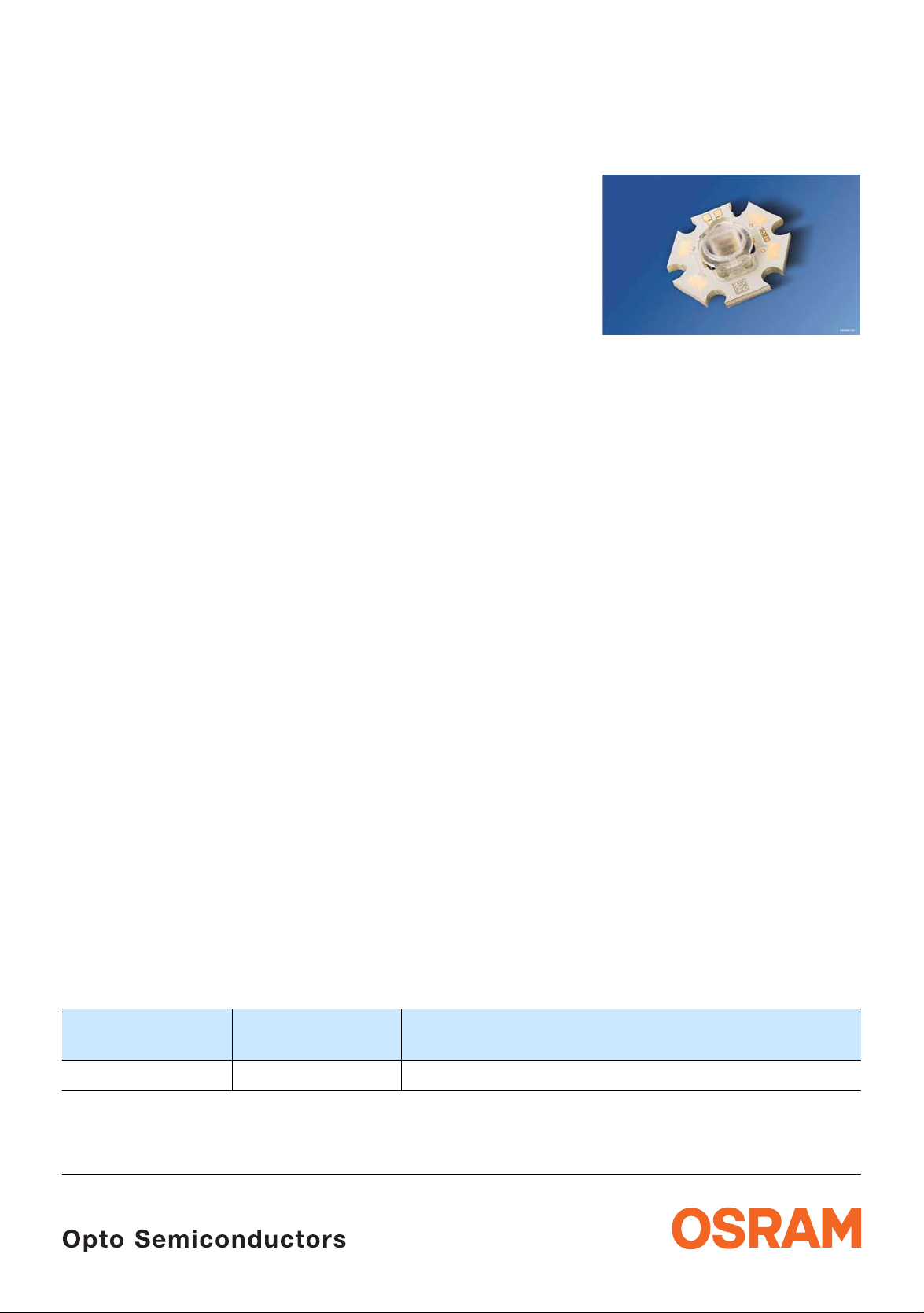
OSTAR
®
- Lighting IR 6-fold with Optics (940nm)
Lead (Pb) Free Product - RoHS Compliant
SFH 4751
Wesentliche Merkmale
•3.1 W optische Leistung bei IF=1A
• Aktive Chipfläche 2.1 x 3.2 mm
2
• max. Gleichstrom 1 A
• niedriger Wärmewiderstand (3 K/W)
• Emissionswellenlänge 940 nm
• ESD-sicher bis 2 kV nach JESD22-A114-B
Anwendungen
• Infrarotbeleuchtung für Kameras
• Überwachungssysteme
• IR-Datenübertragung
• Verkehrsüberwachungssysteme
• Beleuchtung für Bilderkennungssysteme
• Nicht für Anwendungen im Automobilbereich
Sicherheitshinweise
Je nach Betriebsart emittieren diese Bauteile
hochkonzentrierte, nicht sichtbare InfrarotStrahlung, die gefährlich für das menschliche
Auge sein kann. Produkte, die diese Bauteile
enthalten, müssen gemäß den Sicherheitsrichtlinien der IEC-Normen 60825-1 und 62471
behandelt werden.
Features
•3.1 W optical power at IF=1A
• Active chip area 2.1 x 3.2 mm2
• max. DC-current 1 A
• Low thermal resistance (3 K/W)
• Spectral emission at 940 nm
• ESD save up to 2 kV acc. to JESD22-A114-B
Applications
• Infrared Illumination for cameras
• Surveillance systems
• IR Data Transmission
• Intelligent Transportation Systems
• Machine vision systems
• Not released for automotive applications
Safety Advices
Depending on the mode of operation, these
devices emit highly concentrated non visible
infrared light which can be hazardous to the
human eye. Products which incorporate these
devices have to follow the safety precautions
given in IEC 60825-1 and IEC 62471.
Typ
Type
Bestellnummer
Ordering Code
Strahlstärke1) (IF = 1A, tp = 20 ms)
Radiant intensity
1)
Ιe (mW/sr)
SFH 4751 Q65110A8867 > 630 (typ. 900)
1)
gemessen bei einem Raumwinkel Ω = 0.01 sr / measured at a solid angle of Ω = 0.01 sr.
2010-02-15 1
SFH 4751
Grenzwerte T
1)
= 25 °C
B
Maximum Ratings
Bezeichnung
Parameter
Betriebs- und Lagertemperatur
Operating and storage temperature range
Sperrschichttemperatur
Junction temperature
Sperrspannung
Reverse voltage
Vorwärtsgleichstrom
Forward current
Stoßstrom, tp = 100 µs, D = 0
Surge current
Leistungsaufnahme,
Power consumption
Thermische Verlustleistung
Thermal power-dissipation
Symbol
Symbol
T
, T
B, op
T
J
V
R
I
F
I
FSM
P
tot
P
th
B, stg
Wert
Value
Einheit
Unit
– 40 … + 100 °C
+ 145 °C
0.5 V
1 A
5 A
12 W
10.3 W
Wärmewiderstand Sperrschicht / Bodenplatte
R
thJB
3 K/W
Thermal resistance Junction / Base plate
1)
T
= Temperatur auf der Rückseite der Metallkernplatine / Temperature at the backside of the base plate.
B
Kennwerte (TB = 25 °C)
Characteristics
Bezeichnung
Parameter
Wellenlänge der Strahlung
Symbol
Symbol
λ
peak
Wert
Value
950 nm
Wavelength at peak emission
I
= 1 A, tp = 10 ms
F
Schwerpunkts-Wellenlänge der Strahlung
λ
centroid
940 nm
Centroid wavelength
I
= 1 A, tp = 10 ms
F
Spektrale Bandbreite bei 50% von I
Spectral bandwidth at 50% of I
IF = 1 A, t
= 10 ms
p
max
Abstrahlwinkel
max
Δλ 35 nm
ϕ ± 70 Grad
Half angle
Einheit
Unit
deg.
2010-02-15 2
Kennwerte (TB = 25 °C)
Characteristics (cont’d)
SFH 4751
Bezeichnung
Parameter
Abmessungen der aktiven Chipfläche1)
Dimension of the active chip area
Schaltzeiten, Ie von 10% auf 90% und von 90%
I
auf 10%,
= 5 A, RL = 50 Ω
F
Symbol
Symbol
L × B
L × W
t
, t
r
f
Switching times, Ιe from 10% to 90% and from
I
90% to 10%,
Durchlassspannung
= 5 A, RL = 50 Ω
F
V
F
Forward voltage
I
= 1 A, tp = 100 µs
F
Gesamtstrahlungsfluss
Φ
e
Total radiant flux
I
= 1 A, tp = 100 μs
F
Temperaturkoeffizient von Ie bzw. Φ
Temperature coefficient of Ie or Φ
I
= 1 A, tp = 10 ms
F
Temperaturkoeffizient von V
Temperature coefficient of V
I
= 1 A, tp = 10 ms
F
e
F
F
Temperaturkoeffizient von λ
e
TC
TC
TC
I
V
λ,centroid
Temperature coefficient of λ
I
= 1 A, tp = 10 ms
F
1)
Die aktive Chipfläche besteht aus 6 einzelnen Chips mit je 1 x 1 mm².
The active chip area consists of 6 single chips with 1 x 1 mm² each.
Wert
Value
Einheit
Unit
2.1 × 3.2 mm²
10, 10 ns
9.8 (< 12) V
3.1 W
– 0.3 %/K
– 12 mV/K
+ 0.3 nm/K
2010-02-15 3

OHF04180
0˚ 20˚ 40˚ 60˚ 80˚ 100˚ 120˚0.40.60.81.0
100˚
90˚
80˚
70˚
60˚
50˚
0˚10˚20˚30˚40˚
0
0.2
0.4
0.6
0.8
1.0
ϕ
Strahlstärke1) Ι
e
Radiant Intensity1) Ι
Bezeichnung
Parameter
SFH 4751
e
Symbol Werte
Values
SFH 4751 -EA SFH 4751 -EB
Einheit
Unit
Strahlstärke
Radiant Intensity
I
= 1 A, tp = 20 ms
F
1)
Nur eine Gruppe in einer Verpackungseinheit (Streuung kleiner 1.6:1)
Only one group in one packing unit (variation lower 1.6:1)
Ι
e min
Ι
e max
630
1000
Abstrahlcharakteristik
Radiation Characteristics I
= f (ϕ)
rel
800
1250
mW/sr
mW/sr
2010-02-15 4

SFH 4751
800
0
nm
%
OHF04133
20
40
60
80
100
1050850 900 950
I
rel
λ
0
0
˚C
T
I
F
A
OHF04168
0.2
0.4
0.6
0.8
1.0
1.2
B
20 40 60 80 120
OHF04169
F
I
V
A
5
F
V
10
1
10
-2
5
10
-1
5
10
0
7 9 11 13 15 17
0
-5
F
I
A
t
p
s
OHF04167
-410-310-210-1100101102
1010
P
t
=
D
T
T
t
P
I
F
0.01
0.33
0.5
0.2
0.1
0.02
D
0.005
=
0.05
0.5
1.0
1.5
2.0
2.5
3.0
3.5
4.0
4.5
5.5
1
OHF03848
10
-3
A
10
1
0
10
5
5
10
-1
-2
5
10
I
F
10 10
0
10
1
1055
-2 -1
Φ
(1 A)
Φ
e
e
Relative spektrale Emission
Relative Spectral Emission
I
= f (λ), TB = 25 °C
rel
Max. zulässiger Durchlassstrom
Max. Permissible Forward Current
I
= f (TB), R
F
2010-02-15 5
thJB
= 3 K/W
Durchlassstrom
Forward Current
I
= f (VF), TB = 25 °C,
F
Single pulse, tp = 100 μs
Zulässige Impulsbelastbarkeit
Permissible Pulse Handling
Capability
I
= f (tp), T
F
= 85 °C,
B
Duty cycle D = parameter
Relativer Gesamtstrahlungsfluss
Relative Total Radiant Flux
Φe/Φe(1A) = f (IF), TB = 25 °C,
Single pulse, tp = 100 μs

Anschlusskontaktierung
Contacting
SFH 4751
Drahttyp
Wire type
AWG 18 ~0.8 mm
AWG 20 ~0.5 mm
AWG 22 ~0.3 mm
Durchmesser
Diameter
(Litze;
flexible wire)
(Litze;
flexible wire)
(Litze;
flexible wire)
Lötspitze
Solder Tip
3.2 mm
(Meisel;
Chisel)
3.2 mm
(Meisel;
Chisel)
3.2 mm
(Meisel;
Chisel)
Temperatur
Temperature
250 °C
350 °C
250 °C
350 °C
250 °C
350 °C
Lötzeit
Solder Time
16 sec.
6 sec
14 sec.
5 sec
9 sec.
3 sec
2010-02-15 6

Maßzeichnung und Ersatzschaltbild
Package Outlines and equivalent circuit diagram
SFH 4751
Maße in mm (inch) / Dimensions in mm (inch).
Published by OSRAM Opto Semiconductors GmbH
Leibnizstraße 4, D-93055 Regensburg
www.osram-os.com
© All Rights Reserved.
The information describes the type of component and shall not be considered as assured characteristics.
Terms of delivery and rights to change design reserved. Due to technical requirements components may contain
dangerous substances. For information on the types in question please contact our Sales Organization.
Packing
Please use the recycling operators known to you. We can also help you – get in touch with your nearest sales office.
By agreement we will take packing material back, if it is sorted. You must bear the costs of transport. For packing
material that is returned to us unsorted or which we are not obliged to accept, we shall have to invoice you for any costs
incurred.
Components used in life-support devices or systems must be expressly authorized for such purpose! Critical
components 1 , may only be used in life-support devices or systems 2 with the express written approval of OSRAM OS.
1
A critical component is a component usedin a life-support device or system whose failure can reasonably be expected
to cause the failure of that life-support device or system, or to affect its safety or effectiveness of that device or system.
2
Life support devices or systems are intended (a) to be implanted in the human body, or (b) to support and/or maintain
and sustain human life. If they fail, it is reasonable to assume that the health of the user may be endangered.
2010-02-15 7
 Loading...