

Leistungsstarke IR-Lumineszenzdiode
High Power Infrared Emitter
Lead (Pb) Free Product - RoHS Compliant
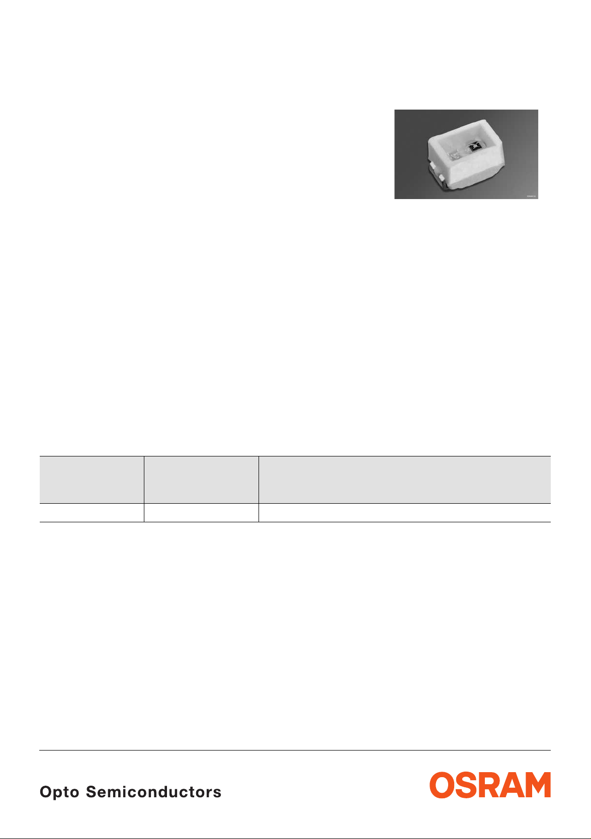
SFH 4203
Wesentliche Merkmale
• Leistungsstarke GaAs-LED (35 mW)
• Hoher Wirkunsgrad bei kleinen Strömen
• Homogene Abstrahlung
• Typische Peakwellenlänge 950 nm
Anwendungen
• Industrieelektronik
• „Messen/Steuern/Regeln“
• Automobiltechnik
• Sensorik
• Alarm- und Sicherungssysteme
• IR-Freiraumübertragung
Typ
Type
SFH 4203 Q65110A2499 8 (> 4)
1)
gemessen bei einem Raumwinkel Ω = 0.01 sr / measured at a solid angle of Ω = 0.01 sr
Bestellnummer
Ordering Code
Strahlstärkegruppierung1) (IF = 100 mA, tp = 20 ms)
Radiant Intensity Grouping
Ie (mW/sr)
Features
• High Power GaAs-LED (35 mW)
• High Efficiency at low currents
• Homogeneous Radiation Pattern
• Typical peak wavelength 950 nm
Applications
• Industrial electronics
• For drive and control circuits
• Automotive technology
• Sensor technology
• Alarm and safety equipment
• IR free air transmission
1)
2005-02-23 1
Grenzwerte (TA = 25 ° C) Maximum Ratings
SFH 4203
Bezeichnung
Parameter
Betriebs- und Lagertemperatur
Operating and storage temperature range
Sperrspannung
Reverse voltage
Durchlassstrom
Forward current
Stoßstrom, tp = 10 µs, D = 0
Surge current
Verlustleistung
Power dissipation
Wärmewiderstand Sperrschicht - Umgebung bei
Montage auf FR4 Platine, Padgröße je 16 mm
2
Thermal resistance junction - ambient mounted
2
on PC-board (FR4), padsize 16 mm
each
Wärmewiderstand Sperrschicht - Lötstelle bei
Montage auf Metall-Block
Thermal resistance junction - soldering point,
mounted on metal block
Symbol
Symbol
T
; T
op
stg
V
R
I
(DC) 100 mA
F
I
FSM
P
tot
R
thJA
R
thJS
Wert
Value
– 40 … + 100 ° C
3 V
1 A
180 mW
450
200
Einheit
Unit
K/W
K/W
Kennwerte (TA = 25 ° C) Characteristics
Bezeichnung
Parameter
Wellenlänge der Strahlung
Wavelength at peak emission
I
= 100 mA, tp = 20 ms
F
Spektrale Bandbreite bei 50% von I
Spectral bandwidth at 50% of I
IF = 100 mA, t
= 20 ms
p
max
Abstrahlwinkel
max
Symbol
Symbol
λ
∆λ 40 nm
ϕ ± 65 Grad
Half angle
Aktive Chipfläche
A
Active chip area
Abmessungen der aktiven Chipfläche
Dimensions of the active chip area
2005-02-23 2
L × B
L × W
peak
Wert
Value
Einheit
Unit
950 nm
deg.
0.09 mm
0.3 × 0.3 mm
2
Kennwerte (TA = 25 ° C)
Characteristics (cont’d)
SFH 4203
Bezeichnung
Parameter
Schaltzeiten, Ie von 10% auf 90% und von 90%
auf 10%, bei
I
= 100 mA, tp = 20 ms, RL = 50 Ω
F
Switching times, Ιe from 10% to 90% and from
I
90% to10%,
= 100 mA, tp = 20 ms, RL = 50 Ω
F
Durchlassspannung
Forward voltage
I
= 100 mA, tp = 20 ms
F
I
= 1 A, tp = 100 µs
F
Sperrstrom
Reverse current
V
= 3 V
R
Gesamtstrahlungsfluss
Total radiant flux
I
= 100 mA, tp = 20 ms
F
Temperaturkoeffizient von Ie bzw. Φe,
I
= 100 mA
F
Temperature coefficient of Ie or Φe,
I
= 100 mA
F
Temperaturkoeffizient von VF, IF = 100 mA
Temperature coefficient of VF, IF = 100 mA
Symbol
Symbol
t
, t
r
f
V
F
V
F
I
R
Φ
e
TC
I
TC
V
Wert
Value
Einheit
Unit
10 ns
1.5 (≤ 1.8)
3.2 (≤ 4.3)
V
V
0.01 (≤ 10) µA
35 mW
– 0.44 %/K
– 1.5 mV/K
Temperaturkoeffizient von λ, IF = 100 mA
TC
Temperature coefficient of λ, IF = 100 mA
Strahlstärke Ie in Achsrichtung
gemessen bei einem Raumwinkel Ω = 0.01 sr
Radiant Intensity Ie in Axial Direction
at a solid angle of Ω = 0.01 sr
Bezeichnung
Symbol Werte
Parameter
Strahlstärke
Radiant intensity
I
= 100 mA, tp = 20 ms
F
Strahlstärke
I
I
I
Radiant intensity
I
= 1 A, tp = 100 µs
F
2005-02-23 3
λ
e min.
e typ.
e typ.
+ 0.2 nm/K
Einheit
Values
4
8
Unit
mW/sr
mW/sr
48 mW/sr

Relative Spectral Emissi on
I
= f (λ)
rel
100
Ι
erel
80
60
OHF00777
I
e
Radiant Intensity
I
e
100 mA
= f (I
F
Single pulse, tp = 20 µs
OHF00809
Ι
e
Ι
e (100 mA)
2
10
0
10
)
Forward Current IF = f (VF)
single pulse, tp = 20 µs
4
10
mA
Ι
F
3
10
2
10
1
10
SFH 4203
OHF00784
40
20
0
850 900 950 1000 1100
nm800
λ
Max. Permissible Forward Current
I
= f (TA), R
F
120
mA
Ι
F
thJA
1)
OHF00359
100
80
R
= 375 K/W
thJA
60
40
20
0
0
20 40 60 80 100 120
˚C
T
A
-1
10
-2
10
-3
10
10 10110
23
10
Radiatio n C h arac t er is ti cs I
50˚
60˚
70˚
80˚
90˚
100˚
1.0 0.8 0.6 0.4
10
mA
Ι
F
= f (ϕ)
rel
0
10
-1
10
-2
10
40
0˚10˚20˚40˚ 30˚
ϕ
1.0
0.8
0.6
0.4
0.2
0
0˚ 20˚ 40˚ 60˚ 80˚ 100˚ 120˚
-3
10
0
0.5 1 1.5 2 2.5 3 3.5 4.5
V
V
F
OHL00869
1)
Thermal resistance junction ambient mounted on PC-board
(FR4), pad size 16 mm
2
(each).
2005-02-23 4
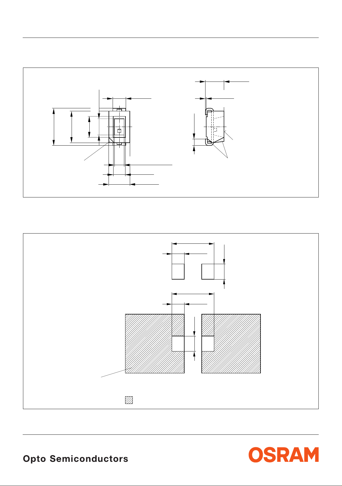
Maßzeichnung Package Outlines
2.1 (0.083)
2.1 (0.083)
2.3 (0.091)
1.2 (0.047)
1.5 (0.059)
1.9 (0.075)
1.0 (0.039)
0.8 (0.031)
0.15 (0.006)
0.05 (0.002)
0.5 (0.020)
0.3 (0.012)
SFH 4203
1.4 (0.055)
1.2 (0.047)
Light emitting area
typ. 1.5 (0.059) x 1.0 (0.039)
Anode
marking
0.8 (0.031)
1.0 (0.039)
+0.05 (0.002)
Anode marking
1.5 (0.059)
1.3 (0.051)
Maße in mm, wenn nicht anders angegeben / Dimensions in m m , un les s oth erw is e s pec if ied.
Empfohlenes Lötpaddesign IR-Reflow Löten Recommended Solder Pad IR Reflow Soldering
2.8 (0.110)
0.8 (0.031)
1 (0.039)
2.8 (0.110)
0.8 (0.031)
Padgeometrie
für verbesserte
Wärmeableitung
1 (0.039)
GPLY6070
Paddesign
for improved
heat dissipation
Cu-Fläche > 16 mm
Cu-area > 16 mm
Maße in mm, wenn nicht anders angegeben / Dimensions in m m , un les s oth erw is e s pec if ied.
2005-02-23 5
2
2
Lötstopplack
Solder resist
OHLPY978
SFH 4203
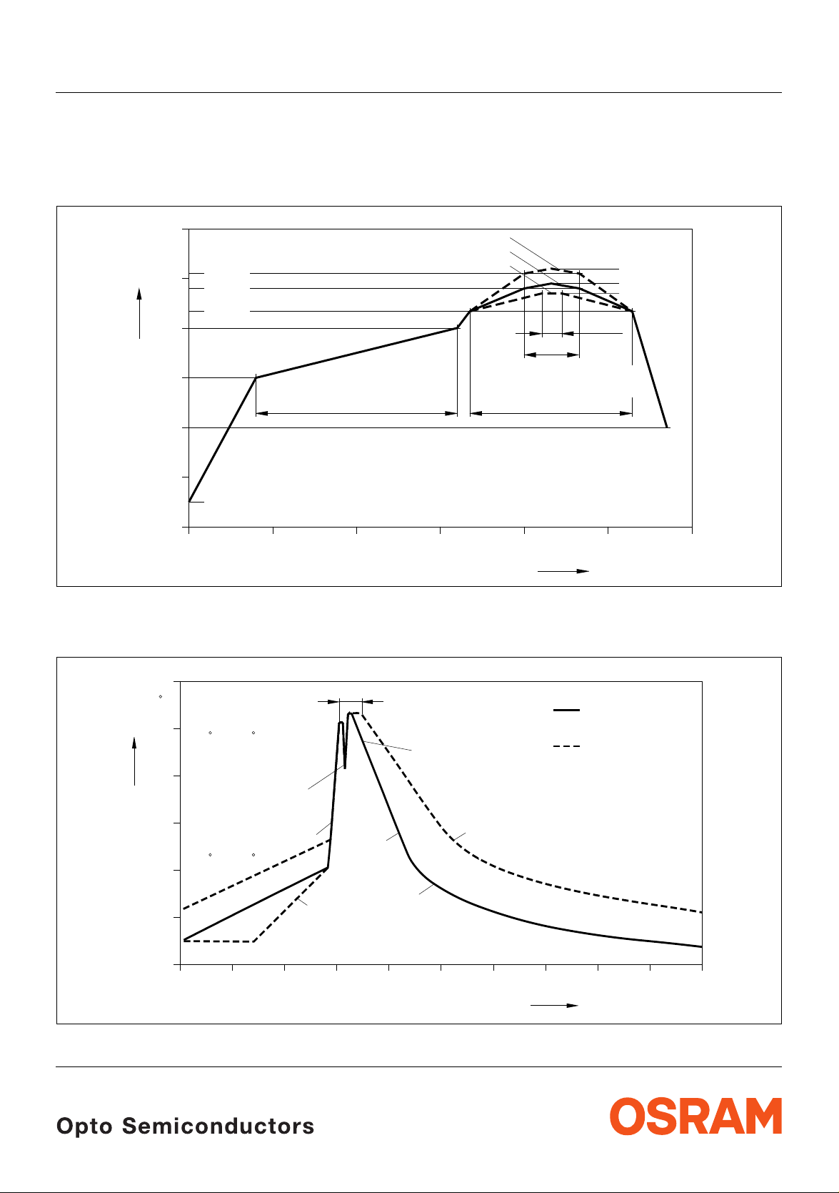
Lötbedingungen Vorbehandlung nach JEDEC Level 2 Soldering Conditions Preconditioning acc. to JEDEC Level 2 IR-Reflow Lötprofil für bleifreies Löten (nach J-STD-020B) IR Reflow Soldering Profile for lead free soldering (acc. to J-STD-020B)
300
˚C
250
T
255 ˚C
240 ˚C
Maximum Solder Profile
Recommended Solder Profile
Minimum Solder Profile
217 ˚C
200
10 s min
30 s max
150
120 s max
100 s max
Ramp Down
6 K/s (max)
100
Ramp Up
50
3 K/s (max)
25 ˚C
0
0
50 100 150 200 250 300
t
Wellenlöten (TTW) (nach CECC 00802) TTW Soldering (acc. to CECC 00802)
OHLA0687
260 ˚C
245 ˚C
235 ˚C
+0 ˚C
-5 ˚C
±5 ˚C
+5 ˚C
-0 ˚C
s
300
C
250
T
235 C
200
150
100
50
0
0
C... 260
1. Welle
1. wave
ca 200 K/s
CC... 130100
50 100 150 200 250
10 s
Zwangskühlung
2 K/s
forced cooling
5 K/s
2005-02-23 6
2. Welle
2. wave
OHLY0598
Normalkurve
standard curve
Grenzkurven
limit curves
2 K/s
s
t
SFH 4203
Published by
OSRAM Opto Semiconductors GmbH
Wernerwerkstrasse 2, D-93049 Regensburg
www.osram-os.com
© All Rights Reserved.
The information describes the type of component and shall not be considered as assured characteristics.
Terms of delivery and rights to change design reserved. Due to technical requirements components may contain
dangerous substances . For in fo rmation on the types in question please contact our Sales Organizati on.
Packing
Please use the recycling operators k nown to you . We can als o help you – get in touch wit h your near est sales offic e.
By agreement we will take p acking material back, if it is sorted. You m ust bear the costs of transport. For packing
material that is returned to us unsorted or which we are not obliged to accept, we shall have to invoice you for any costs
incurred.
Components used in life-su pport devices or systems must be expressly authorized fo r such purpose! Critical
components
1
A critical component is a co mponent usedin a l ife-support devi ce or system whose failure can re asonably be expec ted
1
, may only be used in life-support devices or systems 2 with the express written approval of OSRAM OS.
to cause the failure of that life-support device or system, or to affect its safety or effectiveness of that device or system.
2
Life support devices or systems are intend ed (a) to be impl anted i n t he human b ody , or (b ) to supp ort a nd/or ma inta in
and sustain human life. If th ey fail , it is rea so nable to assume that the health of the us er m ay be endangered.
2005-02-23 7
 Loading...