

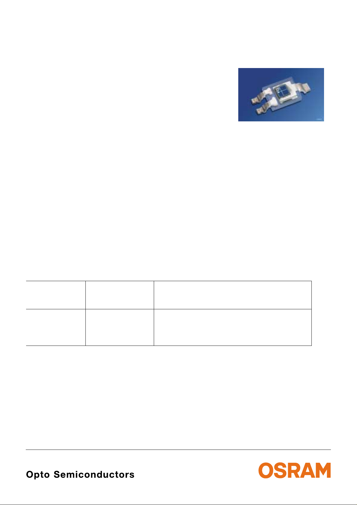
NPN-Si-Fototransistor mit V
Charakteristik
λ
Silicon NPN Phototransistor with V
SFH 3410
Characteristics
λ
Wesentliche Merkmale
• Speziell geeignet für Anwendungen im Bereich
von 350 nm bis 970 nm
V
• Angepaßt an die Augenempfindlichkeit (
)
λ
• SMT-Bauform ohne Basisanschluß, geeignet
für Vapor Phase-Löten und IR-Reflow-Löten
(JEDEC level 4)
• Nur gegurtet lieferbar
Anwendungen
• Umgebungslicht-Detektor
• Beleuchtungsmesser
• Dimmungssensor für Hintergrundbeleuchtung
• „Messen/Steuern/Regeln“
Typ
Type
Bestellnummer
Ordering Code
Fotostrom
Photocurrent
Ipce (
SFH 3410
SFH 3410 -1/2
SFH 3410 -2/3
SFH 3410 -3/4
Q62702-P5160
Q65110A0049
Q65110A0050
Q65110A0051
>3.2
3.2…10
5…16
8…25
Features
• Especially suitable for applications from
350 nm to 970 nm
• Adapted to human eye sensitivity (
V
λ
• SMT package without base connection,
suitable for vapor phase an d IR reflow soldering
(JEDEC level 4)
• Only available on tape and reel
Applications
• Ambient light detector
• Exposure meter for daylight and artificial light
• Sensor for Backlight-Dimming
• For control and drive circuits
tSilicon NPN Phototransistor with Vλ Characteristics
E
= 20 lx, Standard light A, VCE = 5 V
v
µA)
)
2002-12-18 1
Grenzwerte (TA = 25 °C)
Maximum Ratings
SFH 3410
Bezeichnung
Parameter
Betriebs- und Lagertemperatur
Operating and storage temperature range
Kollektor-Emitterspannung
Collector-emitter voltage
Kollektorstrom
Collector current
Emitter-Kollektorspannung
Emitter-collector voltage
T
Kennwerte (
= 25 °C)
A
Characteristics
Bezeichnung
Parameter
Wellenlänge der max. Fotoempfindlichkeit
Wavelength of max. sensitivity
Spektraler Bereich der Fotoempfindlichkeit
S = 10% von S
max
Spectral range of sensitivity
S = 10% of S
max
Bestrahlungsempfindliche Fläche
Radiant sensitive area
Symbol
Symbol
T
; T
op
stg
V
CE
I
C
V
EC
Symbol
Symbol
λ
Smax
Wert
Value
Einheit
Unit
– 40 … + 100 °C
5.5 V
20 mA
0.5 V
Wert
Value
Einheit
Unit
570 nm
λ 350 … 970 nm
A
0.29 mm
2
Abmessung der Chipfläche
Dimensions of chip area
Halbwinkel
L × B
L
ϕ± 60 Grad.
Half angle
Kapazität,
V
= 0 V, f = 1 MHz, E = 0
CE
C
Capacitance
Dunkelstrom
I
Dark current
V
= 5 V
R
Fotostrom
I
Photocurrent
E
= 20 lx, Normlicht/standard light A, VCE = 5 V
v
2002-12-18 2
× W
CE
CEO
PCE
0.75 × 0.75 mm × mm
deg.
16 pF
3 (< 50) nA
>3.2 µA

SFH 3410
Bezeichnung
Parameter
Fotostrom
Photocurrent
E
= 20 lx, Normlicht/standard light A
v
V
= 5 V
CE
Kollektor-Emitter-Sättigungsspannung
Collector-emitter saturation voltage
I
= I
C
1)
I
PCEmin
1)
I
PCEmin
Directional Characteristics S
50
60
1)
PCEmin
× 0.3, EV = 20 lx
ist der minimale Fotostrom der jew eiligen Gruppe
is the min. photocurrent of the spe c ifie d group
= f (ϕ)
rel
40 30 20 10
0
ϕ
1.0
0.8
0.6
Symbol
Symbol
I
PCE
V
CEsat
Wert
Value
Einheit
Unit
-1 -2 -3 -4
3.2…6.3 5…10 8…16 12.5…25 µA
100 100 100 100 mV
OHF01402
70
80
90
100
0.4
0.2
0
0
20 40 60 80 100 1200.40.60.81.0
2002-12-18 3

SFH 3410
Relative Spectral Sensi tivity
S
= f (λ)
rel
100
%
S
rel
80
70
60
50
40
30
20
10
4000500 600 700 800 900 nm 1100
V
λ
OHF00851
λ
Collector-Emitter Current
I
= f (VCE; EV)
CE
80
µ
A
70
I
CE
60
50
40
30
20
10
0
0
200 lx
100 lx
20 lx
1 2 3 4 5
OHF00854
V
CE
Photocurrent
I
= f (EV), VCE = 5 V
PCE
1000
A
µ
I
PCE
100
10
1
1
Photocurrent
E
= 20 lx, VCE = 1 V … 5V
v
1.8
I
PCE
I
PCE (25 ˚C)
1.4
1.2
1.0
0.8
0.6
0.4
0.2
V
0
-50
I
PCE/IPCE(25 °C)
-30 -10 10 30 50 90
OHF00852
lx10 100 1000
E
V
= f (TA)
OHF01024
˚C
T
A
Collector-Emitter Capacitance
C
= f (VCE)
CE
C
18
pF
CE
14
12
10
8
6
4
2
0
10 10
-2
-1
OHF00853
0
10
V
CE
101V
2002-12-18 4

Maßzeichnung
Package Outlines
1.15 (0.045)
0.95 (0.037)
4.8 (0.189)
4.4 (0.173)
Chip position
0.2 (0.008)
0.3 (0.012)
0.1 (0.004)
SFH 3410
0.0 (0.000)
Active area
0.29 mm
2
(not connected)
0.6 (0.024)
0.2 (0.008)
0.5 (0.020)
0.3 (0.012)
2.1 (0.083)
0.9 (0.035)
1.1 (0.043)
1.9 (0.075)
2.7 (0.106)
EmitterCollector
2.5 (0.098)
GEOY6028
0.6 (0.024)
0.8 (0.031)
Maße werden wie folgt ange geben: mm (inch) / Dimensions are specified as follows: mm (inch).
Published by OSRAM Opto Semiconductors GmbH & Co. OHG
Wernerwerkstrasse 2, D-93049 Regensburg
© All Rights Reserved.
Attention please!
The information describes the type of component and shall not be c ons idered as assured characteris tics .
Terms of delivery and rights to change design reserved. Due to technical requirements components may contain
dangerous substances. For information on the types in question please contact our Sales Organization.
Packing
Please use the recycling operators k nown to you . We can als o help you – get in touch wit h your near est sales offic e.
By agreement we will take p acking material back, if it is sorted. You m ust bear the costs of transport. For packing
material that is returned to us unsorted or which we are not obliged to accept, we shall have to invoice you for any costs
incurred.
Components used in life-su pport devices or systems must be expressly authorized fo r such purpose! Critical
components
1
A critical component is a co mponent usedin a l ife-support devi ce or system whose failure can re asonably be expec ted
to cause the failure of that l ife- support devi ce or s ystem, or to affect its s afet y or ef fective ness o f t hat devi ce or syste m.
2
Life support devices or systems are intend ed (a) to be impl anted i n t he human b ody , or (b ) to supp ort a nd/or ma inta in
and sustain human life. If th ey fail , it is rea so nable to assume that the health of the us er m ay be endangered.
1
, may only be used in life-support devices or systems 2 with the express written approval of OSRAM OS.
0.2 (0.008)
0.6 (0.024)
2002-12-18 5
 Loading...