

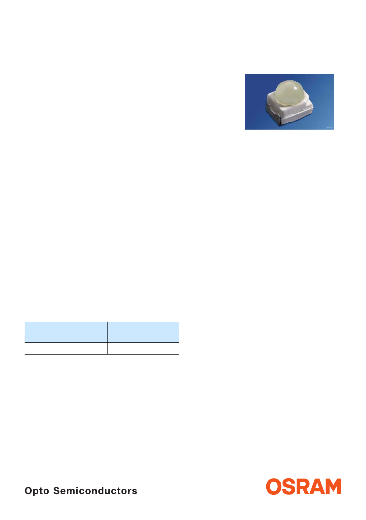
NPN-Silizium-Fototransistor in SMT-Gehäuse mit Linse
Silicon NPN Phototransistor in SMT-Package with lens
Lead (Pb) Free Product - RoHS Compliant
SFH 3219
Wesentliche Merkmale
• TOPLED mit Linse
• Speziell geeignet für Anwendungen im Bereich
von 430
• Hohe Linearität
• Für alle Lötverfahren geeignet
• Gehäusegleich mit SFH 4209, SFH 4219,
SFH
Anwendungen
• Miniaturlichtschranken für Gleich- und
Wechsellichtbetrieb
• Industrieelektronik
• „Messen/Steuern/Regeln“
• Automobiltechnik
• Sensorik
Typ
Type
SFH 3219 Q65110A2529
nm bis 1150 nm
4289
Bestellnummer
Ordering Code
Features
• TOPLED with lens
• Especially suitable for applications from
nm to 1150 nm
430
• High linearity
• Suitable for all soldering methods
• Same package as SFH 4209, SFH 4219,
4289
SFH
Applications
• Miniature photointerrupters
• Industrial electronics
• For control and drive circuits
• Automotive technology
• Sensor technology
2005-04-29 1
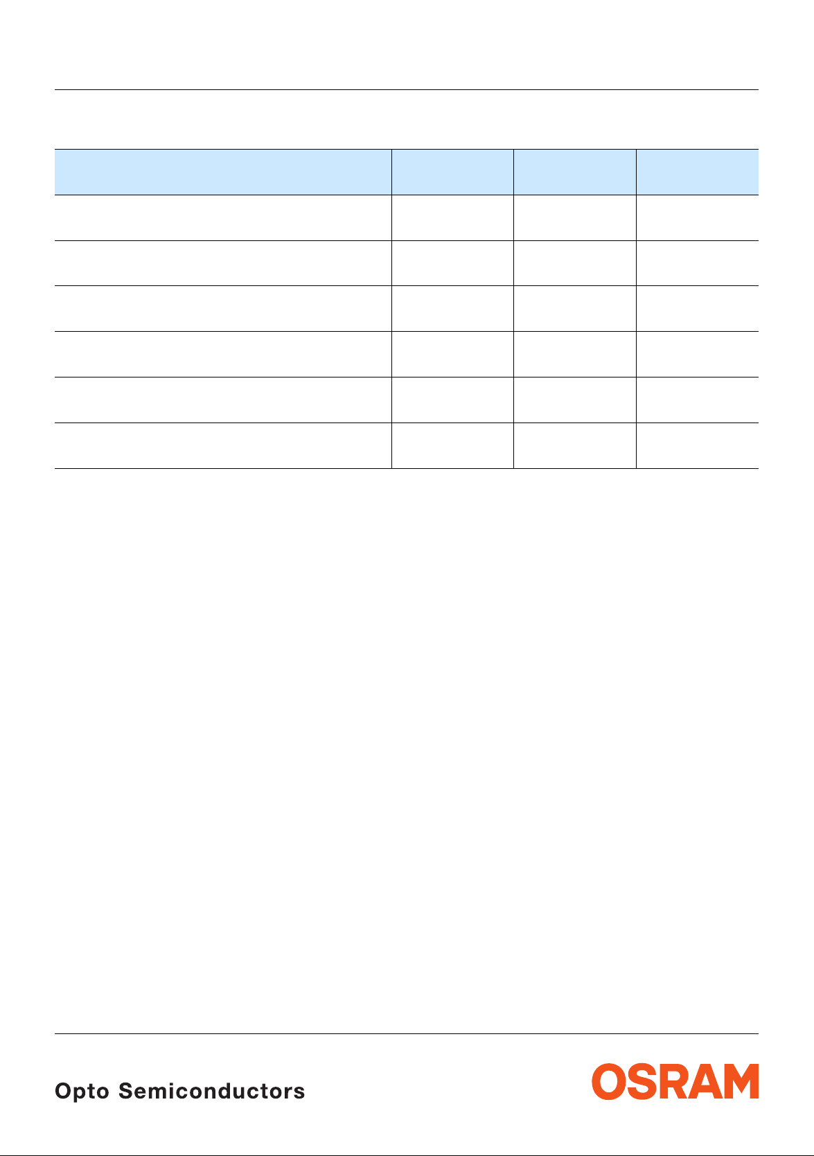
Grenzwerte Maximum Ratings
SFH 3219
Bezeichnung
Parameter
Betriebs- und Lagertemperatur
Operating and storage temperature range
Kollektor-Emitterspannung
Collector-emitter voltage
Kollektorstrom
Collector current
Kollektorspitzenstrom, τ < 10 µs
Collector surge current
Verlustleistung, TA = 25 ° C
Total power dissipation
Wärmewiderstand für Montage auf PC-Board
Thermal resistance for mounting on pcb
Symbol
Symbol
T
; T
op
stg
V
CE
I
C
I
CS
P
tot
R
thJA
Wert
Value
Einheit
Unit
– 40 … + 100 ° C
35 V
15 mA
75 mA
165 mW
450 K/W
2005-04-29 2
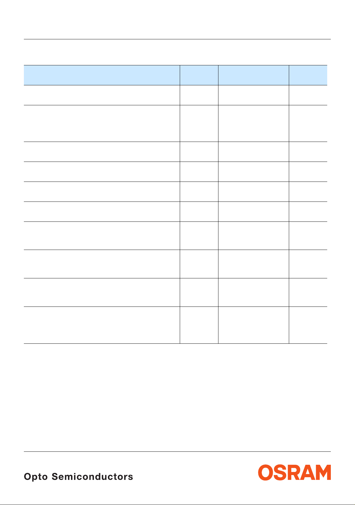
Kennwerte (TA = 25 ° C, λ = 950 nm)
Characteristics
SFH 3219
Bezeichnung
Parameter
Wellenlänge der max. Fotoempfindlichkeit
Wavelength of max. sensitivity
Spektraler Bereich der Fotoempfindlichkeit
S = 10% von S
max
Spectral range of sensitivity
S = 10% of S
max
Bestrahlungsempfindliche Fläche (∅ 240 µm)
Radiant sensitive area
Abmessung der Chipfläche
Dimensions of chip area
Halbwinkel
Half angle
Kapazität, VCE = 0 V, f = 1 MHz, E = 0
Capacitance
Dunkelstrom
Dark current
V
= 20 V, E = 0
CE
Fotostrom
Photo current
E
= 0.1 mW/cm2, VCE = 5 V
e
Anstiegszeit/Abfallzeit
Rise and fall time
I
= 1 mA, VCC = 5 V, RL = 1 kΩ
C
Kollektor-Emitter-Sättigungsspannung
Collector-emitter saturation voltage
I
= 20 µA
C
E
= 0.1 mW/cm
e
2
Symbol
Symbol
λ
S max
Wert
Value
Einheit
Unit
990 nm
λ 430 … 1150 nm
A
L × B
0.045 mm
0.45 × 0.45 mm × mm
2
L × W
ϕ ± 25 Grad
deg.
C
I
I
t
V
CE
CEO
PCE
, t
r
CEsat
f
5.0 pF
1 (≤ 50) nA
≥ 63 µA
7 µs
150 mV
2005-04-29 3
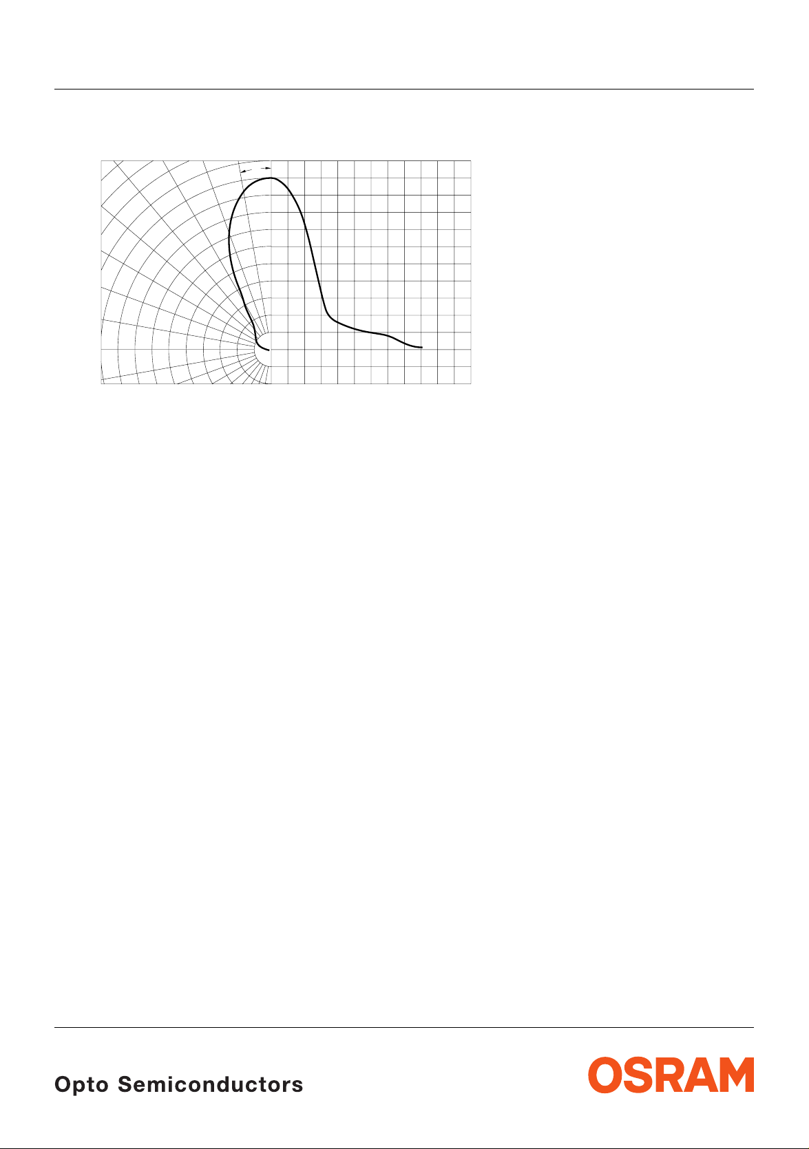
Directional Characteristics
S
= f (ϕ)
rel
SFH 3219
0˚10˚20˚40˚ 30˚
ϕ
1.0
OHF00006
50˚
60˚
70˚
80˚
90˚
100˚
1.0 0.8 0.6 0.4
0.8
0.6
0.4
0.2
0
0˚ 20˚ 40˚ 60˚
80˚
100˚ 120˚
2005-04-29 4
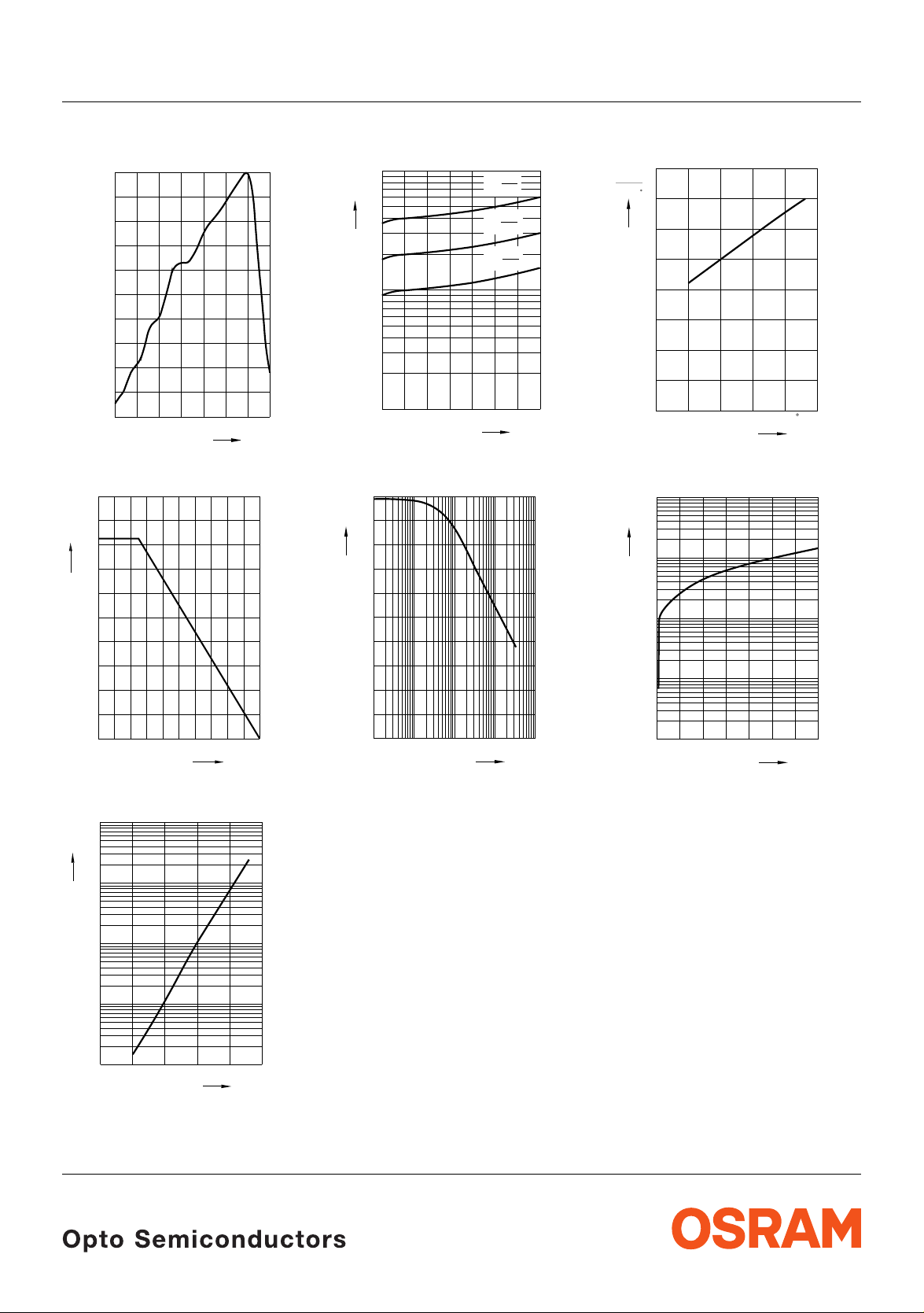
SFH 3219
Relative Spectral Sensitivity
S
= f (λ)
rel
100
%
S
rel
80
OHF00207
70
60
50
40
30
20
10
0
400
500 600 700 800 900 1100
nm
λ
Total Power Dissipation
P
= f (TA)
tot
200
mW
P
tot
160
120
80
40
0
0
20 40 60 80 ˚C 100
OHF00871
T
A
Dark Current
I
= f (TA), VCE = 5 V, E = 0
CEO
Ι
CEO
3
10
OHF01530
Photocurrent
I
= f (VCE), Ee = Parameter
PCE
0
10
mA
Ι
PCE
-1
10
-2
10
0
5 10 15 20 25 30 35
Capacitance
C
= f (VCE), f = 1 MHz, E = 0
CE
5.0
C
pF
CE
4.0
3.5
3.0
2.5
2.0
1.5
1.0
0.5
0
-2
10
10-110010110
0.4
0.2
0.1
OHF00007
mW
2
cm
mW
2
cm
mW
2
cm
V
CE
OHF01528
V
V
CE
Photocurrent
I
PCE /IPCE25°
1.6
Ι
PCE
Ι
PCE
25
1.4
1.0
0.8
0.6
0.4
V
= f (TA), VCE = 5 V
1.2
0.2
0
-25
0 25 50 75 100
OHF01524
C
T
A
Dark Current
I
= f (VCE), E = 0
CEO
1
10
nA
Ι
CEO
0
10
-1
10
-2
10
-3
2
10
0 5 10 15 20 25 30 35V
OHF01527
V
CE
2
10
1
10
0
10
-1
10
-25nA0 25 50 75 100
˚C
T
A
2005-04-29 5
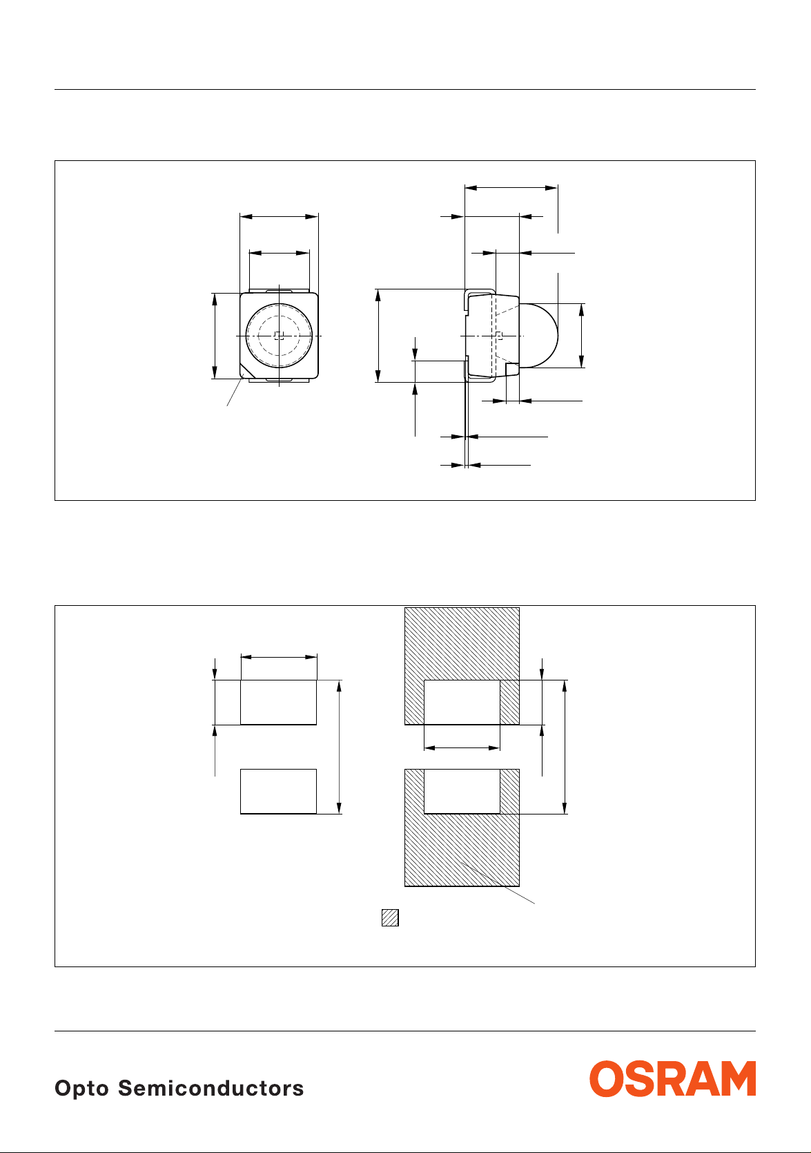
Maßzeichnung Package Outlines
SFH 3219
3.5 (0.138) max.
3.0 (0.118)
2.6 (0.102)
2.3 (0.091)
2.1 (0.083)
1
3.4 (0.134)
3.0 (0.118)
2
Package
marking
Kathodenkennung: abgeschrägte Ecke
Cathode mark: bevelled edge
Empfohlenes Lötpaddesign
Recommended Solderpad Design
3.7 (0.146)
3.3 (0.130)
1.1 (0.043)
2.1 (0.083)
1.7 (0.067)
0.1 (0.004) (typ.)
0.5 (0.020)
0.18 (0.007)
0.13 (0.005)
0.9 (0.035)
0.7 (0.028)
ø2.60 (0.102)
0.6 (0.024)
0.4 (0.016)
GEOY6956
ø2.55 (0.100)
2.6 (0.102)
2.6 (0.102)
1.5 (0.059)
Padgeometrie für
verbesserte Wärmeableitung
Paddesign for
improved heat dissipation
4.5 (0.177)
Lötstopplack
Solder resist
Cu-Fläche > 16 mm
Cu-area > 16 mm
4.5 (0.177)
1.5 (0.059)
2
2
OHLPY970
Maße werden wie folgt angegeben: mm (inch) / Dimensions are specified as follows: mm (inch).
2005-04-29 6
SFH 3219
Lötbedingungen Vorbehandlung nach JEDEC Level 2
Soldering Conditions Preconditioning acc. to JEDEC Level 2
IR-Reflow Lötprofil für bleifreies Löten (nach J-STD-020B)
IR Reflow Soldering Profile for lead free soldering (acc. to J-STD-020B)
300
˚C
250
T
255 ˚C
240 ˚C
Maximum Solder Profile
Recommended Solder Profile
Minimum Solder Profile
217 ˚C
200
10 s min
30 s max
150
120 s max
100 s max
Ramp Down
6 K/s (max)
100
Ramp Up
50
3 K/s (max)
25 ˚C
0
0
50 100 150 200 250 300
Wellenlöten (TTW) (nach CECC 00802)
TTW Soldering (acc. to CECC 00802)
OHLA0687
260 ˚C
245 ˚C
235 ˚C
+0 ˚C
-5 ˚C
±5 ˚C
+5 ˚C
-0 ˚C
s
t
300
C
250
T
200
150
100
235 C
CC... 130100
50
0
0
C... 260
1. Welle
1. wave
ca 200 K/s
50 100 150 200 250
10 s
2 K/s
5 K/s
Zwangskühlung
forced cooling
2005-04-29 7
2. Welle
2. wave
OHLY0598
Normalkurve
standard curve
Grenzkurven
limit curves
2 K/s
s
t

SFH 3219
Published by
OSRAM Opto Semiconductors GmbH
Wernerwerkstrasse 2, D-93049 Regensburg
www.osram-os.com
© All Rights Reserved.
The information describes the type of component and shall not be considered as assured chara cteristics.
Terms of delivery and rights to change design reserved. Due to technical requirements components may contain
dangerous substances. For information on the types in question please contact our Sales Organization.
Packing
Please use the recycling operators known to you. We can also help you – get in touch with your nearest sales office.
By agreement we will take packing material back, if it is sorted. You must bear the costs of transport. For packing
material that is returned to us unsorted or wh ich we are not obliged to accept, we shall hav e to invoice you for any costs
incurred.
Components used in life-support devices or systems must be expressly authorized for such purpose! Critical
components 1 , may only be used in life-support devices or systems 2 with the express written approval of OSRAM OS.
1
A critical component is a component used in a life-support device or sys tem whose failure can reasonably be expected
to cause the failure of that life-support device or system, or to affec t its safety or e ffectiveness of that dev ice or system.
2
Life support devices or systems are intended (a) to be implanted in the h uman body, or (b) to support and/or maintain
and sustain human life. If they fail, it is reasonable to assume that the health of the user may be endangered.
2005-04-29 8
 Loading...