

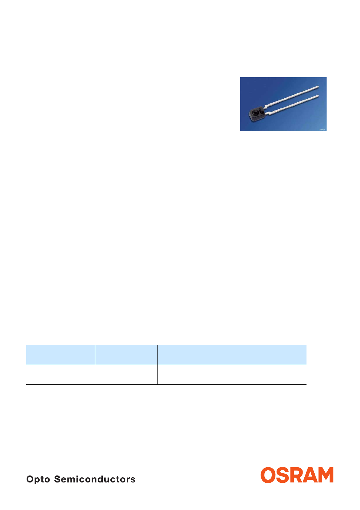
NPN-Silizium-Fototransistor mit Tageslichtsperrfilter
Silicon NPN Phototransistor with Daylight-Cutoff Filter
Lead (Pb) Free Product - RoHS Compliant
SFH 3100 F
Wesentliche Merkmale
• Speziell geeignet für Anwendungen im Bereich
von 840 nm bis 1080 nm
• Enge Empfangscharakteristik
• Geringe Außenabmessungen
• Gleiche Bauform wie IRED SFH 4110
• Hoher Koppelfaktor in Lichtschranken mit
SFH 4110
• IR-Filter
• Leichte Unterscheidbarkeit zwischen
SFH 3100 F (schwarzes Gehäuse) und
SFH 4110 (klares Gehäuse)
Anwendungen
• Empfänger in Lichtschranken
• Bandende-Erkennung (z.B. Videorecorder)
• Datenübertragung
• Positionsüberwachung
• Barcode-Leser
• „Messen/Steuern/Regeln“
• Münzzähler
Features
• Especially suitable for applications from
840 nm to 1080 nm
• Narrow half angle
• Small outline dimensions
• Same package as IRED SFH 4110
• High coupling factor in light barriers with
SFH 4110
• IR filter
• Easy identification of SFH 3100 F (black
package) and SFH 4110 (clear package)
Applications
• Detector in photointerrupters
• Tape end detection
• Data transmission
• Position sensing
• Barcode reader
• For control and drive circuits
• Coin counters
Typ
Type
SFH 3100 F
SFH 3100 F-2/3/4
2005-02-17 1
Bestellnummer
Ordering Code
Q62702P5073
Q62702P5475
I
(mA)
PCE
(λ = 950 nm,
>0.4
0.63 ... 3.2
E
= 0.5 mW/cm2, VCE = 5 V)
e
Grenzwerte
Maximum Ratings
SFH 3100 F
Bezeichnung
Parameter
Betriebs- und Lagertemperatur
Operating and storage temperature range
Kollektor-Emitterspannung
Collector-emitter voltage
Kollektorstrom
Collector current
Kollektorspitzenstrom,
t < 10 µs
Collector surge current
Emitter-Kollektorspannung
Emitter-collector voltage
Verlustleistung,
T
= 25 °C
A
Total power dissipation
Wärmewiderstand Sperrschicht - Umgebung
Thermal resistance junction - ambient
Symbol
Symbol
T
; T
op
stg
V
CE
V
(t <2min)3070
CE
I
C
I
CS
V
EC
P
tot
R
thJA
Wert
Value
Einheit
Unit
– 40 … + 85 °C
V
50 mA
100 mA
7V
150 mW
280 K/W
2005-02-17 2
Kennwerte (TA = 25 °C, λ = 950 nm)
Characteristics
SFH 3100 F
Bezeichnung
Parameter
Wellenlänge der max. Fotoempfindlichkeit
Wavelength of max. sensitivity
Spektraler Bereich der Fotoempfindlichkeit
S = 10% von S
max
Spectral range of sensitivity
S = 10% of S
max
Abmessungen der Chip-Fläche
Dimension of chip area
Bestrahlungsempfindliche Fläche
Radiant sensitive area
Halbwinkel
Half angle
Kapazität
Capacitance
V
= 0 V, f = 1 MHz, E =0
CE
V
= 5 V, f = 1 MHz, E =0
CE
Dunkelstrom,
V
CE
= 20 V
Dark current
Symbol
Symbol
λ
Smax
Wert
Value
Einheit
Unit
920 nm
λ 840 … 1080 nm
L × B
× W
L
0.55 × 0.55 mm × mm
A 0.11 mm
ϕ± 14 Grad
deg.
C
I
CEO
CE
6.5
pF
3.0
2 (≤ 50) nA
2
Fotostrom
Photocurrent
E
= 0.5 mW/cm2,VCE = 5 V
e
I
PCE
>0.4 mA
2005-02-17 3

SFH 3100 F
Bezeichnung
Parameter
Fotostrom, λ = 950 nm
Photocurrent
E
= 0.5 mW/cm2, VCE = 5 V
e
Anstiegszeit/Abfallzeit
Rise and fall time
I
= 1 mA, VCC = 5 V, RL = 1 kΩ
C
Kollektor-Emitter-Sättigungsspannung
Collector-emitter saturation voltage
=
I
I
C
E
= 0.5 mW/cm2, λ = 950 nm
e
1)
I
PCEmin
1)
I
PCEmin
1)
PCEmin
× 0.3,
ist der minimale Fotostrom der jeweiligen Gruppe.
is the min. photocurrent of the specified group.
Symbol
Symbol
I
PCE
t
,
r
t
f
V
CEsat
Wert
Value
Einheit
Unit
-2 -3 -4
0.63 … 1.25 1 … 2 1.6 … 3.2 mA
7
µs
9
110 (≤ 400) mV
2005-02-17 4

SFH 3100 F
Relative Spectral Sensitivity
S
= f (λ)
rel
100
%
S
rel
90
80
70
60
50
40
30
20
10
0
700
800 900 1000 1100nm
I
Photocurrent
V
= 5 V, normalized to 25 °C
CE
1.6
Ι
PCE
Ι
PCE
25
1.4
1.2
PCE
= f (TA),
OHF00377
λ
OHF01524
Photocurrent
I
= f (Ee), VCE = 5 V
PCE
1
10
mA
Ι
PCE
0
10
-1
10
-2
10
-3
10
-3
10
-2
10
Dark Current
I
= f (TA), VCE = 20 V, E = 0
CEO
3
10
Ι
CEO
2
10
10
-1
mW/cm
OHF00378
2
10
E
e
OHF00380
Collector-Emitter Capacitance
C
= f (VCE), f = 1 MHz, E = 0
CE
7
pF
CE
6
5
4
3
2
1
0
0
-2
10C10-1100101102V
OHF00379
V
CE
Total Power Dissipation
P
= f (TA)
tot
160
mW
P
tot
140
120
OHF00381
1.0
0.8
0.6
0.4
0.2
0
-25
0 25 50 75 100
Photocurrent SFH 3100 F
I
= f (VCE)
PCE
2.0
mA
Ι
PCE
1.8
1.6
1.4
1.2
1.0
0.8
0.6
0.4
0.2
0
10 20 30 40V
0
1.0 mW/cm
0.5 mW/cm
0.25 mW/cm
0.1 mW/cm
C
T
A
OHF00386
2
2
2
2
V
CE
1
10
0
10
-1
10
0nA20 40 60 80 100˚C
Dark Current
I
= f (VCE), E = 0
CEO
1
10
nA
Ι
CEO
0
10
-1
10
-2
10
0
T
A
OHF00383
10 20 30V
V
100
80
60
40
20
0
20 40 60 80 100
0
CE
˚C
T
A
2005-02-17 5

Maßzeichnung
Package Outlines
SFH 3100 F
Emitter/
Cathode
2.54 (0.100)
1.42 (0.056)
1.22 (0.048)
0.6 (0.024)
0.5 (0.020)
16.5 (0.650)
16.0 (0.630)
1.04 (0.041)
0.84 (0.033)
17.77 (0.700)
0.4 (0.016)
17.27 (0.680)
0.3 (0.012)
0.9 (0.035)
60˚
0.7 (0.028)
R 0.7 (0.028)
R 0.9 (0.035)
4.1 (0.161)
3.9 (0.154)
1.3 (0.051)
1.1 (0.043)
2.9 (0.114)
3.1 (0.122)
0.5 (0.020) x 45˚
1.04 (0.041)
0.84 (0.033)
1.6 (0.063)
1.4 (0.055)
0.84 (0.033)
2.2 (0.087)
2.0 (0.079)
3.0 (0.118)
2.8 (0.110)
0.64 (0.025)
GEOY6976
Maße werden wie folgt angegeben: mm (inch) / Dimensions are specified as follows: mm (inch).
2005-02-17 6

Empfohlenes Lötpaddesign Wellenlöten (TTW)
Recommended Solder Pad
TTW Soldering
4.8 (0.189)
4 (0.157)
SFH 3100 F
OHLPY985
2005-02-17 7

Lötbedingungen
Soldering Conditions
Wellenlöten (TTW) (nach CECC 00802)
TTW Soldering (acc. to CECC 00802)
SFH 3100 F
300
C
250
T
235 C
200
150
CC... 130100
100
50
0
0
C... 260
1. Welle
1. wave
ca 200 K/s
50 100 150 200 250
10 s
2 K/s
2. Welle
2. wave
5 K/s
Zwangskühlung
forced cooling
Normalkurve
standard curve
Grenzkurven
limit curves
2 K/s
t
OHLY0598
s
Published by
OSRAM Opto Semiconductors GmbH
Wernerwerkstrasse 2, D-93049 Regensburg
www.osram-os.com
© All Rights Reserved.
The information describes the type of component and shall not be considered as assured chara cteristics.
Terms of delivery and rights to change design reserved. Due to technical requirements components may contain
dangerous substances. For information on the types in question please contact our Sales Organization.
Packing
Please use the recycling operators known to you. We can also help you – get in touch with your nearest sales office.
By agreement we will take packing material back, if it is sorted. You must bear the costs of transport. For packing
material that is returned to us unsorted or wh ich we are not obliged to accept, we shall hav e to invoice you for any costs
incurred.
Components used in life-support devices or systems must be expressly authorized for such purpose! Critical
components
1
A critical component is a component used in a life-support device or sys tem whose failure can reasonably be expected
1
, may only be used in life-support devices or systems 2 with the express written approval of OSRAM OS.
to cause the failure of that life-support device or system, or to affec t its safety or e ffectiveness of that dev ice or system.
2
Life support devices or systems are intended (a) to be implanted in the human body , or (b) to support and/or maintain
and sustain human life. If they fail, it is reasonable to assume that the health of the user may be endangered.
2005-02-17 8
 Loading...