

Page 1
www.osram.com/oled
APRIL
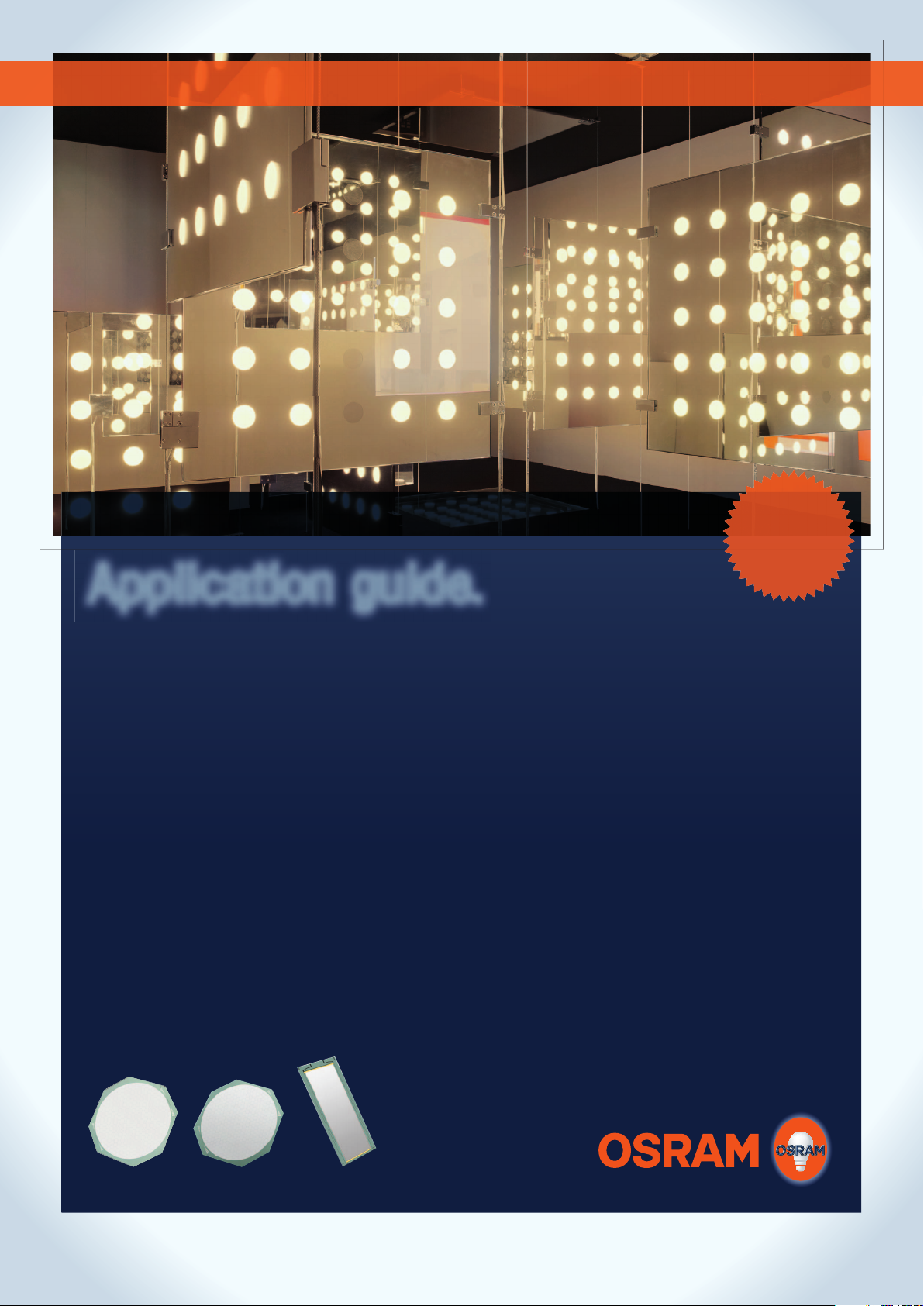
Application guide.
ORBEOS
®
2011
Page 2
CONTENTS
2
Page 3
CONTENTS
1. OLED integration 4
1.1. General handling instructions 4
1.2. Contact ledges and their polarity 5
1.3. Interconnection 6
1.4. Contacting of OLED tiles
via conductive glue 6
1.5. Contacting of OLED tiles
via elastomeric connectors 7
1.6. Contacting via Flex-PCB 8
2. Binning 10
2.1. Color binning 10
2.2. Luminance binning 12
3. Driving 13
4. Reliability 13
4.1. Maximum ratings 13
4.2. Degradation 14
4.2.1. Absolute value of initial luminance 14
4.2.2. Ambient temperature 14
4.3. Lifetime 14
4.4. Robustness 15
4.4.1. Mechanical pressure,
shock and vibration 15
4.4.2. ESD sensitivity 15
4.4.3. Low air pressure 15
4.4.4. Shelf life 15
4.4.5. Photo degradation (UV resistance) 15
Appendix 16
3
Page 4

OLED INTEGRATION
1. OLED integration
1.1. General handling instructions
Remember when handling OLED devices: First and fore-
most, OLEDs are made of glass and glass is fragile.
• Avoid mechanical stress such as shock and pressure on the
glass during handling, especially at the center of the active
area and the back of the device (to avoid glass cracking,
delamination and damage of the internal structure).
• For tiled OLED designs without a frame to protect the edges
and corners of the tile, exercise caution in order to avoid glass
chipping and breakage.
• Finger cots and/or gloves are recommended when handling
OLEDs to avoid corrosion of contacting material.
• In case of a fl ex connector or any other type of connector, do
not pull, press, or peel off the connector from glass contact
area, as this will cause module malfunctions.
• Do not submerge the module into any kind of solvent or
any other chemicals such as (but not limited to) acids,
bases or salts.
• Wipe off water drops. Contact with water over a long period
of time may cause damage to the scattering fi lm on the active
side of the OLED, and an active OLED tile with water conden-
sation on its surface will result in corrosion of metal traces.
• Handle the OLED’s surface (glass or fi lm) with care. Avoid
hard or sharp objects coming into contact with the tile sur-
face. Do not rub hard on the OLED surface.
• Avoid touching exposed contact pads with bare fi ngers, as
this will leave moisture on metal traces and cause corrosion.
• In case of OLED breakage, please avoid direct contact and
handle like broken glass: Use protective gloves to avoid injury.
Use a dust pan and hand brush to dispose of the splinters.
• Keep chips and materials out of reach of children.
• The light-emitting side of the OLED device can be cleaned
by softly wiping the surface with a moist cleaning cloth.
Small amounts of glass cleaner may be used.
4
Page 5
1.2. Contact ledges and their polarity
OLED devices without Flex-PCB (for Flex-PCB, please see
below) are electrically connected via the metallized areas
at the contact ledges (see fi g. 1). Usually, symbols at the
metallization indicate the polarity of the contacts. For round
ORBEOS
contacts can be identifi ed when looking at the emissive side
of the device: Cathode contacts exhibit a comb structure at
the edge of the active area (see fi g. 2). Often, devices have
more than two contact ledges, i.e. there might be more than
one contact ledge for each polarity (see device in fi g. 2).
®
(CDW-031, CMW-031) devices, the cathode
OLED INTEGRATION
The rectangular ORBEOS
ledges, two cathode pads and one anode pad (see fi g. 2c).
All contact ledges must be electrically connected in order to
ensure optimum current supply from all sides necessary for
best brightness homogeneity over the active area. Other
confi gurations will usually lead to a signifi cant reduction of
brightness homogeneity.
®
RMW-046 exhibits three contact
Fig. 1. Rear side of an OLED device. The device is electrically connected at the contact
ledges. Symbols usually indicate the polarity of the contacts.
+
–
–
–
ab c
+
+ +
–
Fig. 2. a) Polarity of a round ORBEOS® CDW-031, CMW-031. b) The cathode contacts exhibit a comb structure. c) The rectangular ORBEOS® RMW-046 has three contact ledges.
5
Page 6
OLED INTEGRATION
1.3. Interconnection
On the following pages, several techniques for interconnec-
ting OLEDs are described. To interconnect OLED devices,
their contact surfaces have to be free of dust and grease.
If necessary, use isopropyl alcohol (IPA) to carefully wipe the
contact ledges clean.
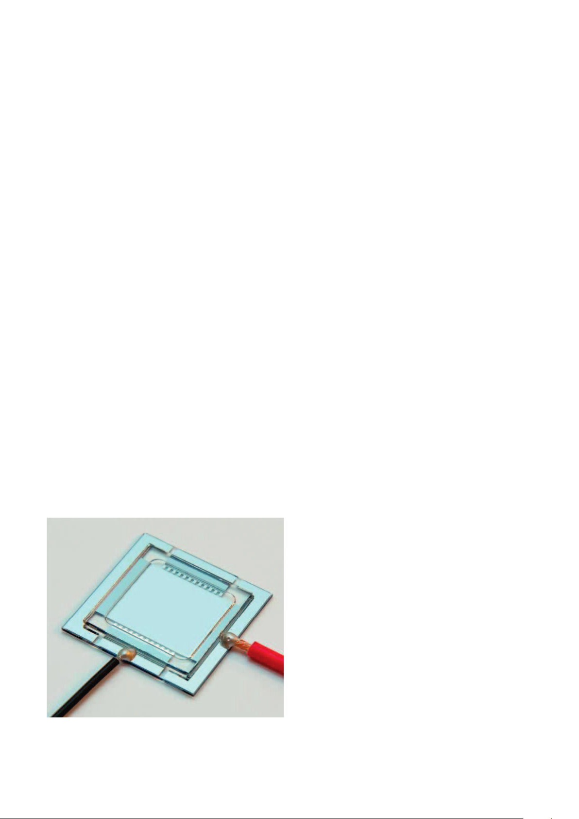
1.4. Contacting of OLED tiles via conductive glue
The conductive epoxy used in this application example can
be obtained through R+S Components (conductive epoxy
CW2400, Stock No.: 496-265).
Mix equal amounts of part A and part B thoroughly for at least
2 minutes. The mixed components have to be applied within
a short period. The pot life is only 10 minutes at 24 °C. After-
wards, apply the epoxy to the contact surface and attach
In general, the interconnection should be applied without heat
introduction into the active area of the device. Furthermore,
avoid mechanical stress. Exercise caution in order to avoid
glass chipping and breakage when applying the interconnec-
tion at the substrate edges.
the wire. For better adhesion, fan out the strands of the wire
slightly before attaching it. The wire should have a cross-
sectional area of 0.25 – 0.5 mm². The curing time of the epoxy
is 4 hours at room temperature (24 °C). However, to achieve
maximum conductivity and adhesion, you may expose the ep-
oxy to a temperature of 66 °C – 80 °C for 10 minutes and sub-
sequently allow it to cool. Please note that the heat should be
applied to the contact ledges only.
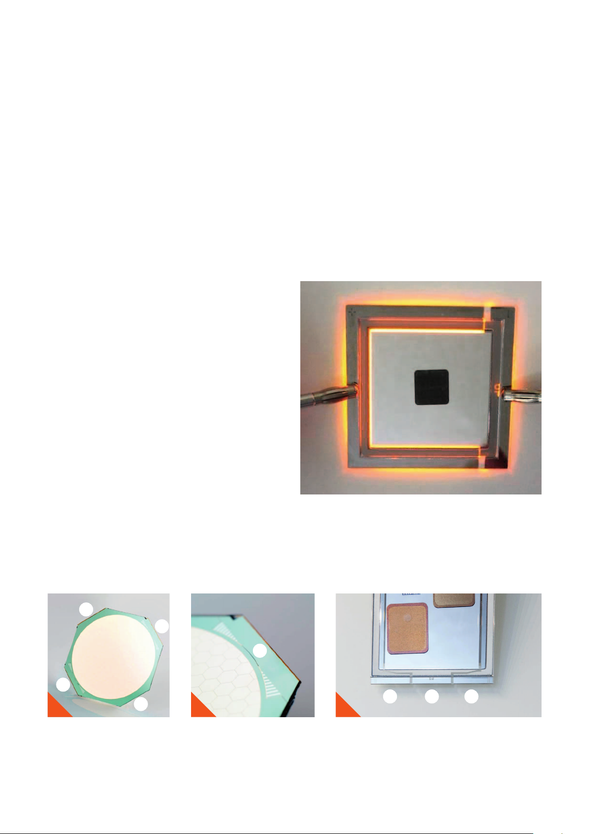
Fig. 3. Rear side of an OLED device. Two wires are attached to the contact ledges with
conductive epoxy.
6
Page 7
1.5. Contacting of OLED tiles via elastomeric connectors
In this example, elastomeric connectors are used for inter-
connecting OLEDs. Similar low-resistance connectors can
be used accordingly. The product can be acquired from
Nucletron Technologies GmbH, Munich.
OLED INTEGRATION
The connectors should cover the contact ledges completely to
minimize contact resistance. They have to be compressed by
5 – 25 % of their height to ensure optimal conductivity and
vibration resistance. The carrier of the OLED has to provide a
suffi cient holding force and also has to fi x the connectors late-
rally. To calculate the force needed, consult the datasheet of
the connectors. Keep in mind that the active area of the OLEDs
should not be exposed to mechanical stress.
F
Fig. 4. Front side of an ORBEOS® CMW-031. The elastomeric connectors (light blue) have to be compressed to ensure suffi cient electrical connection.
7
Page 8

OLED INTEGRATION
abc
Fig. 5. Free-standing Flex-PCB with four fl aps (a) attached to an ORBEOS® CMW-031 (b). The eight golden soldering pads of the Flex-PCB are visible. Each one provides a positive and
negative pole as well as a through contact “0”. ORBEOS
®
RMW-046 (c) can be equipped with a fl ex connector with two soldering pads on both sides (front side and back side).
1.6. Contacting via Flex-PCB
The application of Flex-PCBs (fl exible printed circuit boards)
allows the connection of an OLED device with wires by stan-
dard selective solder process (heat tip). Devices with more
than two contact ledges can be connected by only two wires
without any branches. Furthermore, depending on the de-
sign, Flex-PCBs are bendable due to their low thickness in
the range of 300 µm.
As an example, fi gure 5 shows a Flex-PCB (left) attached to
an ORBEOS
®
CMW-031 (right). The Flex-PCB has four con-
tacts to the OLED and 8 areas for external wiring. Figure 5.
c) illustrates the Flex-PCB of an ORBEOS
®
RMW-046. Several
different wiring modes are possible using the fl ex connector as
shown in fi gure 6.
Fig. 6. a) Single devices (CDW-031, CMW-031)
Fig. 6. Various wiring options. These can be realized with the help of the Flex-PCB
shown in fi gure 5.
8
Fig. 6. b) Series connection (CDW-031, CMW-031)
Fig. 6. c) Series connection with back wiring (CDW-031, CMW-031)
Fig 6. d) Single device and series connection (RMW-046)
Page 9
OLED INTEGRATION
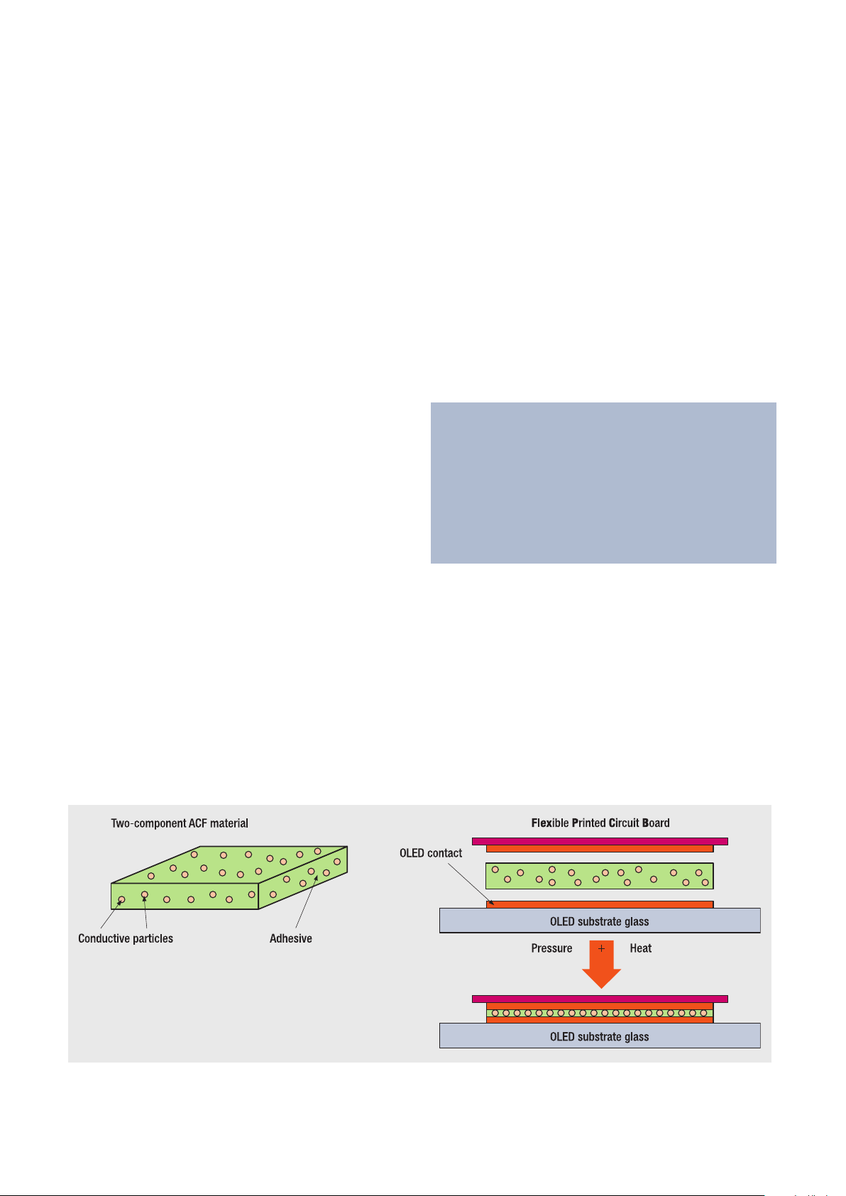
Flex-PCBs are applied by a special conductive polymer mate-
rial in a thermo-compression process called ACF bonding
(anisotropic conductive fi lm bonding), which is well known
from the display industry: First, a two-component material is
dispensed at the contact pad of the OLED. Then, the Flex-PCB
is adjusted to the contact pad. Afterwards, heat and pressure
is applied on the connection by a heated stamp (bonding
tool, fi gure 7).
ORBEOS
®
devices are available with PCB. In case an indivi-
dual PCB design is desired, and for more details on the
material and process conditions, the following links regarding
ACF may be helpful:
http://www.hitachi-chem.co.jp/english/products/do/001.html
http://www.sonycid.jp/en/products/dd1/
For more details on ACF/heatseal bonding equipment, please
refer to, e.g.:
http://www.miyachieurope.com/products/hot-bar/
Thermal management:
Heat sinks as known from LED technology are not obligatory, since
OLEDs are cooled passively by heat convection and radiation from
both of their surfaces. A device, which is driven at typical operation
conditions (1000 cd/m
2
luminance), heats up by between 5 K and
15 K above ambient temperature. In general, the design of the OLED
application should enable suffi cient heat transport from the surfaces.
Please also see the section: 4.2.2. Ambient temperature.
Fig. 7. Application of Flex-PCB on the OLED contacts via ACF bonding.
9
Page 10

BINNING
2. Binning
Solid-state lighting products are usually classifi ed into color and
brightness bins in order to meet customer demands and deliver
as narrow selections as possible. For ORBEOS
binning schemes are explained in the following sections.
2.1. Color binning
®
products, the
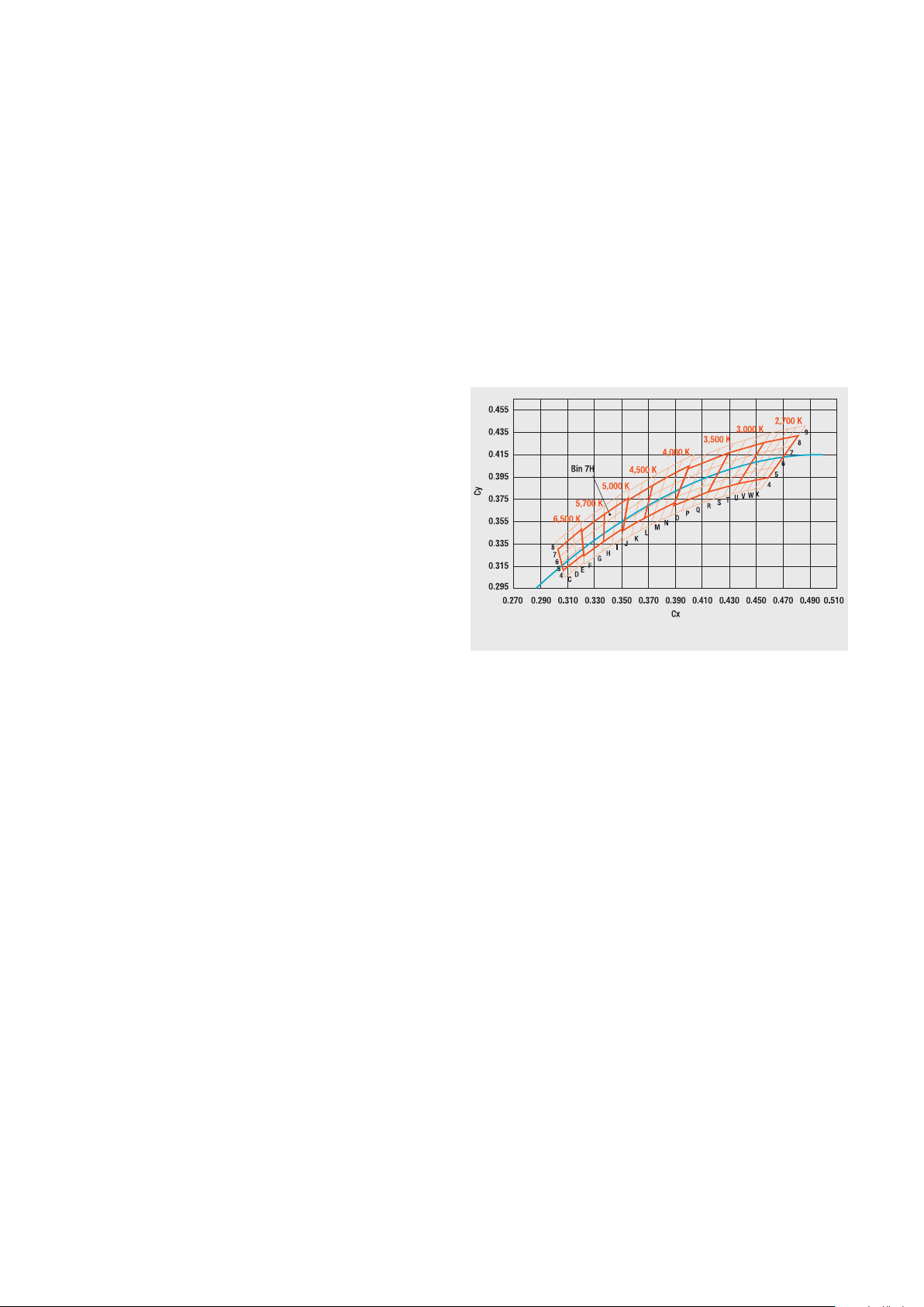
A widely-used standard for the classifi cation of chromaticity
in SSL application is “ANSI_NEMA_ANSLG C78.377-2008”
(http://www.nema.org/stds/ANSI-ANSLG-C78-377.cfm).
In this document, standard color temperatures are defi ned
and described as boxes along the Planck curve (as shown
Fig. 8. ANSI-NEMA classifi cation of SSL color temperature boxes.
in fi gure 8).
The corner and center points of these boxes are addressed as follows:
2,700 K 3,000 K 3,500 K 4,000 K 4,500 K 5,000 K 5,700 K 6,500 K
xyxyxyxyxyxyx yxy
Center
point
Tolerance
quadrangle
0.4578 0.4101 0.4338 0.4030 0.4073 0.3917 0.3818 0.3797 0.3611 0.3658 0.3447 0.3553 0.3287 0.3417 0.3123 0.3282
0.4813 0.4319 0.4562 0.4260 0.4299 0.4165 0.4006 0.4044 0.3736 0.3874 0.3551 0.3760 0.3376 0.3616 0.3205 0.3481
0.4562 0.4260 0.4299 0.4165 0.3996 0.4015 0.3736 0.3874 0.3548 0.3736 0.3376 0.3616 0.3207 0.3462 0.3028 0.3304
0.4373 0.3893 0.4147 0.3814 0.3889 0.3690 0.3670 0.3578 0.3512 0.3465 0.3366 0.3369 0.3222 0.3243 0.3068 0.3113
0.4593 0.3944 0.4373 0.3893 0.4147 0.3814 0.3839 0.3716 0.3670 0.3578 0.3515 0.3487 0.3366 0.3369 0.3221 0.3261
Table 1: CIE x/y coordinates of corners and centers of the ANSI-NEMA boxes.
10
Page 11
OSRAM has established a fi ner resolution classifi cation and
has divided the ANSI-NEMA color boxes into smaller sub-bins
(so called “fi ne-bins”). In order to cover the full production
output, a row of sub-bins of similar size have been introduced
above and below the ANSI-NEMA boxes. The scheme is
shown in fi gure 9.
BINNING
In this binning scheme, the size of one fi ne-bin box roughly
corresponds to a three-step MacAdam ellipse. According
to MacAdam, a one-step ellipse in the CIE 1931 diagram
represents an area where a homogeneous color impression
is perceived (MacAdam, D. L., Visual sensitivities to color dif-
ferences in daylight, J. Opt. Soc. Am., 32, 247 (1942)) and
where color differences are just noticeable to human observers.
The nomenclature of the fi ne-bins is set up as follows. The
resulting grid pattern is created by rows – enumerated from
4 to 8 (and 9, respectively) towards the top – and by columns
assigned from left to right with characters ranging from C to
X. The fi ne-bin is addressed via a combination of row num-
ber and column character. The example in fi gure 9 highlights
the bin 7H. The chromaticity coordinates of the fi ne-bins are
given in the appendix.
Since it is impossible to produce only one selected bin, an order
has to combine several fi ne-bins. The more parts are needed,
the more fi ne-bins have to be selected in order to ensure se-
curity of supply. Individual selections can be agreed upon in
close cooperation with each customer.
Fig. 9. OSRAM Opto Semiconductors’ fi ne binning scheme of white color.
11
Page 12

BINNING
2.2. Luminance binning
Brightness binning of OLEDs is slightly different than for LED
products. While inorganic LEDs rely on luminous intensity or
a fi ner classifi cation. Detailed values of upper and lower bin
limits are shown in table 2.
luminous fl ux binning, the most reasonable quantity for OLED
products is the luminance. For ORBEOS
®
products, the binning
scheme is characterized by a double-digit system. The fi rst digit
denotes the rough luminance class. The second digit delivers
ORBEOS
defi ned by the constant drive current. For example, the
ORBEOS
Luminance class 1st digit: Luminance class Luminance range 2nd digit: Fine-bin Binning code
250 cd/m
500 cd/m
1,000 cd/m
2,000 cd/m
4,000 cd/m
Upper limit
2
cd/m
2
2
2
2
2
1 200 230 1
1 230 265 2
1 265 305 3
1 305 350 4
1 350 400 5
2 400 460 1
2 460 530 2
2 530 610 3
2 610 700 4
2 700 800 5
3 800 920 1
3 920 1,060 2
3 1,060 1,220 3
3 1,220 1,400 4
3 1,400 1,600 5
4 1,600 1,840 1
4 1,840 2,120 2
4 2,120 2,440 3
4 2,440 2,800 4
4 2,800 3,200 5
5 3,200 3,680 1
5 3,680 4,240 2
5 4,240 4,880 3
5 4,880 5,600 4
5 5,600 6,400 5
Lower limit
cd/m
®
products are usually set to a nominal luminance
®
CDW-031 is a typical 1000 cd/m² product.
2
11
12
13
14
15
21
22
23
24
25
31
32
33
34
35
41
42
43
44
45
51
52
53
54
55
Table 2: Limit values of luminance bins.
12
Page 13

3. Driving
DRIVING/RELIABILITY
In general, OLEDs are driven in constant current mode. If
dimming is required, it is recommended to use PWM (pulse
width modulation). Besides, it is also possible to adjust the
driving current. Please note that current modulation may in-
fl uence the color coordinates of the emitted light.
If several OLEDs are supposed to light up simultaneously, a
series connection has to be used. Parallel connection may
result in different luminance values or even cause damage of
the devices. OLEDs are designed for driving under forward
voltage only. Please avoid any kind of reverse voltage applied
to the OLED.
4. Reliability
4.1. Maximum ratings
The core materials of an OLED device are organic semicon-
ductor compounds which currently cannot be used under
extreme conditions. OSRAM defi ned some generic maximum
ratings for the operation of ORBEOS
in table 3.
®
products as described
If a constant-current source design for LEDs is used, make
sure that the power supply doesn’t generate current and/or
voltage overshoots while switching it on or off.
Parameter Value
Relative humidity 40 °C/93 %
Operating temperature range -20 … +40 °C
These ratings can also be found on the datasheets. Stresses
beyond the conditions listed in this table or the dedicated
datasheet may cause permanent damage to the device.
Stresses at maximum rating conditions for extended periods
may affect the device reliability. This may include optical arti-
facts and sudden failure modes such as shorts as well as
faster luminance degradation.
Storage temperature range -40 … +60 °C
Operating and storage pressure 0.8 … 1.2 bar
Table 3: OLED maximum ratings.
13
Page 14

RELIABILITY
1.00
0.75
0.50
0.25
Relative luminance [L/L0]
0
0 2,500 5,000 7,500 10,000 12,500 15,000 17,500
Fig. 10. Luminance degradation characteristics of an OLED with two different initial
luminance values (normalized luminance values). The lower curve shows a drop to
50 % of the initial value after approximately 5,000 hours. By reducing the initial luminance by a factor of 2, the time to reach the half value nearly triples to 14,000
hours (upper curve).
Operating time [h]
Initial luminance = 50 % of standard
Standard initial luminance
4.2. Degradation
The major type of degradation during operation which can be
observed quite easily is the decay of luminance. Driven under
constant current conditions, the luminance of an OLED typi-
cally degrades according to a stretched exponential behavior,
meaning that the initial degradation rate is higher than the
degradation rate in the mid or later state of operation. The
luminance degradation effect is dependent on several side
parameters:
4.2.1. Absolute value of initial luminance
The higher the luminance of the OLED, the more charge car-
riers are transported through the device which can initiate
degradation mechanisms. Additionally, the internal OLED
temperature increases due to higher energy input resulting in
an accelerated degradation. Depending on the stack archi-
tecture, the effect can be more or less pronounced. As a rule
of thumb, it can be estimated that the lifetime can be tripled
when the initial luminance is decreased by 50 %. This is indi-
cated in fi gure 10 (above).
In parallel to the luminance decay, the driving voltage will in-
crease during operation in constant current mode. ORBEOS®
OLEDs currently show a voltage increase of less than 1.0 V
after reaching 50 % of the initial luminance.
4.2.2. Ambient temperature
The luminance degradation is a process which requires acti-
vation energy. This means that for higher ambient temperature,
the decay rate is also higher. As another rule of thumb, it can
be estimated that a temperature increase of about 20 K cur-
rently leads to reduction of lifetime by approximately 50 %.
Since the OLED is sensitive to higher temperatures, a heat man-
agement system is recommended in order to keep operating
temperature low and the lifetime of the OLED high. Depending
on the individual integration level, e.g. in a well-insulated envi-
ronment, accumulation of heat needs to be avoided.
4.3. Lifetime
The luminance degradation is the most important parameter
for the defi nition of lifetime and reliability. For a single OLED
device, the lifetime is usually defi ned as the time interval in
which the luminance has dropped to a certain percentage of
its initial value. The operating conditions (constant current
driving, ambient temperature etc.) remain unchanged during
this period of time.
14
Most common in use are L50 and L70 values, representing
the time intervals after which 50 % and 70 % of the initial
luminance values have been reached. In contrast to other
light sources the luminance is taken as reference quantity
and not luminous intensity or luminous fl ux, because for a
large area emitter the luminance can be determined easier
and quicker.
Page 15

4.4. Robustness
RELIABILITY
In the following paragraphs, some indications are given on
the ruggedness of OLEDs and their stability against some
environmental conditions.
4.4.1. Mechanical pressure, shock and vibration
OLEDs are made of glass, meaning that mechanical forces
may cause glass breaks. One special case is local pressure
on the back side of a cavity-glass-encapsulated OLED. Even
with quite low forces (just by using a fi nger) the cap glass
may be bended and touches the cathode of the OLED caus-
ing damage to the device. Such handling must be avoided
during assembly of the OLED. For a thin-fi lm-encapsulated
device, this issue is irrelevant. OSRAM has tested various
OLEDs and their resistance against shock and vibration. The
table below shows the tested conditions. There is no concern
to use OLEDs under these conditions.
4.4.2. ESD sensitivity
OLEDs represent a big capacitance. However, they are not
designed for reverse operation. The organic layer structure
is very thin, meaning that high electrical fi elds can occur in
case of electrostatic discharge. According to the human body
model (HBM), OLEDs can withstand 1 kV. Proper grounding
should be assured when handling OLEDs during luminaire
assembly. In order to ensure maximum ESD stability, all
ORBEOS
equipped with an ESD protection diode.
®
panels with fl ex connectors from OSRAM are
4.4.3. Low air pressure
The maximum ratings on the datasheet state 800 mbar as
minimum pressure. Actually, the OLEDs can withstand lower
air pressures, e.g. while transporting them on a plane. The
limit must be mentioned in case of glass-cavity-encapsulated
OLEDs. The glass cavity is fi lled with an inert gas at standard
ambient pressure. By decreasing the outer pressure, the dif-
ference between inner and outer pressure may cause a lift-
off of the cap glass from the substrate. However, the exact
values for the limit pressures change with the size of the
OLED. In case of a thin-fi lm-encapsulated OLED, this issue
is irrelevant.
4.4.4. Shelf life
Shelf life denotes the length of time a product may be stored
without becoming unsuitable for use. Under ambient condi-
tions (room temperature, 50 % RH, no direct exposure to
sunlight etc.) it is typically 10 years. Increased temperature
may reduce shelf life.
4.4.5. Photo degradation (UV resistance)
OLEDs are currently designed for indoor applications.
Test Condition Duration
Mechanical vibration Displacement: 0.35 mm
10 sweeps per X, Y, Z direction
Acceleration: 5 g
Frequency: 10 – 500 Hz
Mechanical shock 11 ms half sine
6 shocks per X, Y, Z direction
100 g peak
15
Page 16
APPENDIX
Appendix
Corner values (CIE coordinates) of all 4C9X fi ne-bins
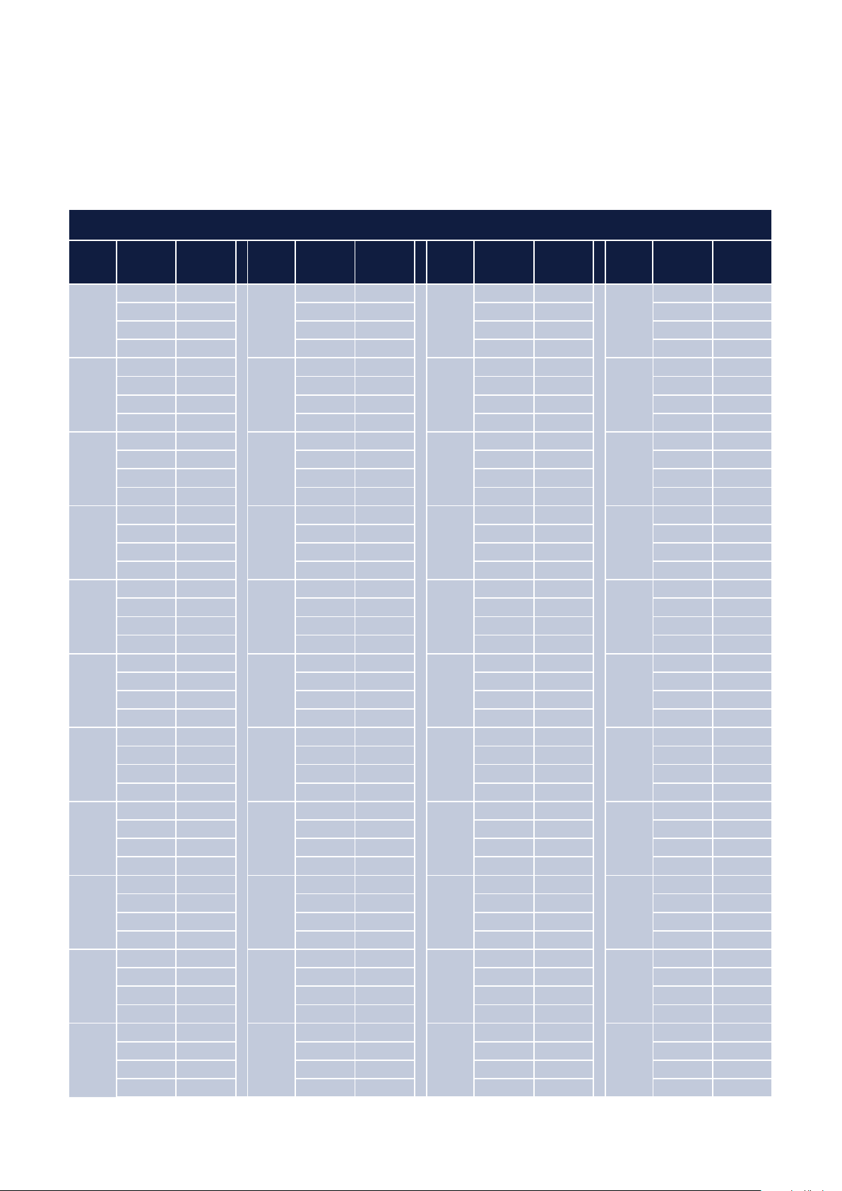
Bin cx cy Bin cx cy Bin cx cy Bin cx cy
8C 0.3028 0.3304 8J 0.3548 0.3736 9Q 0.4198 0.4115 9W 0.4688 0.429
0.3015 0.3368 0.356 0.3826 0.4232 0.4201 0.4739 0.4382
0.3076 0.343 0.3659 0.3899 0.4337 0.4253 0.4803 0.4398
0.3087 0.3363 0.3642 0.3805 0.4299 0.4165 0.475 0.4304
7C 0.3041 0.324 7J 0.3536 0.3646 8Q 0.4164 0.4029 8W 0.4636 0.4197
0.3028 0.3304 0.3548 0.3736 0.4198 0.4115 0.4688 0.429
0.3087 0.3363 0.3642 0.3805 0.4299 0.4165 0.475 0.4304
0.3098 0.3296 0.3625 0.3711 0.4261 0.4077 0.4697 0.4211
6C 0.3055 0.3177 6J 0.3524 0.3555 7Q 0.4129 0.3944 7W 0.4585 0.4104
0.3041 0.324 0.3536 0.3646 0.4164 0.4029 0.4636 0.4197
0.3098 0.3296 0.3625 0.3711 0.4261 0.4077 0.4697 0.4211
0.3108 0.3229 0.3608 0.3616 0.4223 0.3989 0.4644 0.4118
5C 0.3068 0.3113 5J 0.3512 0.3465 6Q 0.4095 0.3858 6W 0.4534 0.4011
0.3055 0.3177 0.3524 0.3555 0.4129 0.3944 0.4585 0.4104
0.3108 0.3229 0.3608 0.3616 0.4223 0.3989 0.4644 0.4118
0.3119 0.3162 0.3591 0.3522 0.4185 0.3902 0.4591 0.4024
4C 0.3081 0.3049 4J 0.35 0.3375 5Q 0.4061 0.3773 5W 0.4483 0.3918
0.3068 0.3113 0.3512 0.3465 0.4095 0.3858 0.4534 0.4011
0.3119 0.3162 0.3591 0.3522 0.4185 0.3902 0.4591 0.4024
0.313 0.3095 0.3574 0.3427 0.4147 0.3814 0.4538 0.3931
8D 0.3087 0.3363 8K 0.3642 0.3805 4Q 0.4027 0.3687 4W 0.4432 0.3826
0.3076 0.343 0.3659 0.3899 0.4061 0.3773 0.4483 0.3918
0.3138 0.3492 0.3758 0.3973 0.4147 0.3814 0.4538 0.3931
0.3146 0.3422 0.3736 0.3874 0.4109 0.3726 0.4485 0.3838
7D 0.3098 0.3296 7K 0.3625 0.3711 9R 0.4299 0.4165 9X 0.475 0.4304
0.3087 0.3363 0.3642 0.3805 0.4337 0.4253 0.4803 0.4398
0.3146 0.3422 0.3736 0.3874 0.4428 0.4286 0.4868 0.4413
0.3154 0.3352 0.3714 0.3775 0.4387 0.4197 0.4813 0.4319
6D 0.3108 0.3229 6K 0.3608 0.3616 8R 0.4261 0.4077 8X 0.4697 0.4211
0.3098 0.3296 0.3625 0.3711 0.4299 0.4165 0.475 0.4304
0.3154 0.3352 0.3714 0.3775 0.4387 0.4197 0.4813 0.4319
0.3162 0.3282 0.3692 0.3677 0.4346 0.4108 0.4758 0.4225
5D 0.3119 0.3162 5K 0.3591 0.3522 7R 0.4223 0.3989 7X 0.4644 0.4118
0.3108 0.3229 0.3608 0.3616 0.4261 0.4077 0.4697 0.4211
0.3162 0.3282 0.3692 0.3677 0.4346 0.4108 0.4758 0.4225
0.317 0.3212 0.367 0.3578 0.4304 0.4018 0.4703 0.4132
4D 0.313 0.3095 4K 0.3574 0.3427 6R 0.4185 0.3902 6X 0.4591 0.4024
0.3119 0.3162 0.3591 0.3522 0.4223 0.3989 0.4644 0.4118
0.317 0.3212 0.367 0.3578 0.4304 0.4018 0.4703 0.4132
0.3178 0.3142 0.3648 0.3479 0.4263 0.3929 0.4648 0.4038
8E 0.3146 0.3422 8L 0.3736 0.3874 5R 0.4147 0.3814 5X 0.4538 0.3931
0.3138 0.3492 0.3758 0.3973 0.4185 0.3902 0.4591 0.4024
0.32 0.3554 0.3853 0.4033 0.4263 0.3929 0.4648 0.4038
0.3205 0.3481 0.3826 0.3931 0.4222 0.384 0.4593 0.3944
16
Page 17

APPENDIX
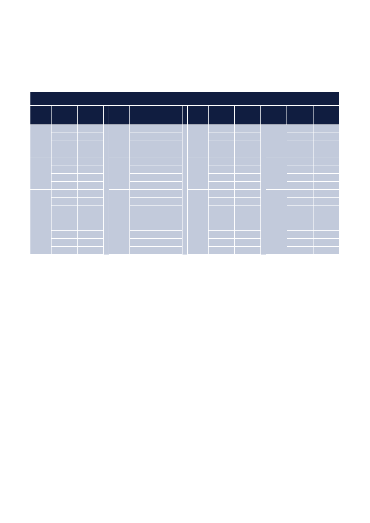
Corner values (CIE coordinates) of all 4C9X fi ne-bins
Bin cx cy Bin cx cy Bin cx cy Bin cx cy
7E 0.3154 0.3352 7L 0.3714 0.3775 4R 0.4109 0.3726 4X 0.4485 0.3838
0.3146 0.3422 0.3736 0.3874 0.4147 0.3814 0.4538 0.3931
0.3205 0.3481 0.3826 0.3931 0.4222 0.384 0.4593 0.3944
0.321 0.3408 0.3799 0.3828 0.4181 0.3751 0.4538 0.385
6E 0.3162 0.3282 6L 0.3692 0.3677 9S 0.4387 0.4197
0.3154 0.3352 0.3714 0.3775 0.4428 0.4286
0.321 0.3408 0.3799 0.3828 0.4518 0.4319
0.3216 0.3334 0.3773 0.3726 0.4474 0.4228
5E 0.317 0.3212 5L 0.367 0.3578 8S 0.4346 0.4108
0.3162 0.3282 0.3692 0.3677 0.4387 0.4197
0.3216 0.3334 0.3773 0.3726 0.4474 0.4228
0.3221 0.3261 0.3746 0.3624 0.443 0.4138
4E 0.3178 0.3142 4L 0.3648 0.3479 7S 0.4304 0.4018
0.317 0.3212 0.367 0.3578 0.4346 0.4108
0.3221 0.3261 0.3746 0.3624 0.443 0.4138
0.3226 0.3188 0.3719 0.3522 0.4386 0.4047
8F 0.3207 0.3462 8M 0.3826 0.3931 6S 0.4263 0.3929
0.3202 0.3535 0.3853 0.4033 0.4304 0.4018
0.3291 0.3617 0.3947 0.4093 0.4386 0.4047
0.3291 0.3539 0.3916 0.3987 0.4342 0.3957
7F 0.3212 0.3389 7M 0.3799 0.3828 5S 0.4222 0.384
0.3207 0.3462 0.3826 0.3931 0.4263 0.3929
0.3291 0.3539 0.3916 0.3987 0.4342 0.3957
0.3292 0.3461 0.3885 0.3882 0.4298 0.3867
6F 0.3217 0.3316 6M 0.3773 0.3726 4S 0.4181 0.3751
0.3212 0.3389 0.3799 0.3828 0.4222 0.384
0.3292 0.3461 0.3885 0.3882 0.4298 0.3867
0.3293 0.3384 0.3853 0.3776 0.4253 0.3776
5F 0.3222 0.3243 5M 0.3746 0.3624 9T 0.4474 0.4228
0.3217 0.3316 0.3773 0.3726 0.4518 0.4319
0.3293 0.3384 0.3853 0.3776 0.4609 0.4352
0.3294 0.3306 0.3822 0.367 0.4562 0.426
4F 0.3227 0.317 4M 0.3719 0.3522 8T 0.443 0.4138
0.3222 0.3243 0.3746 0.3624 0.4474 0.4228
0.3294 0.3306 0.3822 0.367 0.4562 0.426
0.3295 0.3228 0.3791 0.3564 0.4515 0.4168
8G 0.3291 0.3539 8N 0.3916 0.3987 7T 0.4386 0.4047
0.3291 0.3617 0.3947 0.4093 0.443 0.4138
0.3379 0.3698 0.4042 0.4153 0.4515 0.4168
0.3376 0.3616 0.4006 0.4044 0.4467 0.4076
7G 0.3292 0.3461 7N 0.3885 0.3882 6T 0.4342 0.3957
0.3291 0.3539 0.3916 0.3987 0.4386 0.4047
0.3376 0.3616 0.4006 0.4044 0.4467 0.4076
0.3373 0.3534 0.397 0.3935 0.442 0.3985
17
Page 18

APPENDIX
Corner values (CIE coordinates) of all 4C9X fi ne-bins
Bin cx cy Bin cx cy Bin cx cy Bin cx cy
6G 0.3293 0.3384 6N 0.3853 0.3776 5T 0.4298 0.3867
0.3292 0.3461 0.3885 0.3882 0.4342 0.3957
0.3373 0.3534 0.397 0.3935 0.442 0.3985
0.3369 0.3451 0.3934 0.3825 0.4373 0.3893
5G 0.3294 0.3306 5N 0.3822 0.367 4T 0.4253 0.3776
0.3293 0.3384 0.3853 0.3776 0.4298 0.3867
0.3369 0.3451 0.3934 0.3825 0.4373 0.3893
0.3366 0.3369 0.3898 0.3716 0.4326 0.3801
4G 0.3295 0.3228 4N 0.3791 0.3564 9U 0.4562 0.426
0.3294 0.3306 0.3822 0.367 0.4609 0.4352
0.3366 0.3369 0.3898 0.3716 0.4674 0.4367
0.3363 0.3287 0.3862 0.3607 0.4625 0.4275
8H 0.3376 0.3616 9O 0.3996 0.4015 8U 0.4515 0.4168
0.3379 0.3698 0.4023 0.4096 0.4562 0.426
0.3471 0.3775 0.4128 0.4148 0.4625 0.4275
0.3464 0.3688 0.4097 0.4065 0.4576 0.4182
7H 0.3373 0.3534 8O 0.3969 0.3934 7U 0.4467 0.4076
0.3376 0.3616 0.3996 0.4015 0.4515 0.4168
0.3464 0.3688 0.4097 0.4065 0.4576 0.4182
0.3456 0.3601 0.4067 0.3982 0.4526 0.409
6H 0.3369 0.3451 7O 0.3943 0.3852 6U 0.442 0.3985
0.3373 0.3534 0.3969 0.3934 0.4467 0.4076
0.3456 0.3601 0.4067 0.3982 0.4526 0.409
0.3448 0.3515 0.4036 0.3898 0.4477 0.3998
5H 0.3366 0.3369 6O 0.3916 0.3771 5U 0.4373 0.3893
0.3369 0.3451 0.3943 0.3852 0.442 0.3985
0.3448 0.3515 0.4036 0.3898 0.4477 0.3998
0.344 0.3428 0.4006 0.3815 0.4428 0.3906
4H 0.3363 0.3287 5O 0.3889 0.369 4U 0.4326 0.3801
0.3366 0.3369 0.3916 0.3771 0.4373 0.3893
0.344 0.3428 0.4006 0.3815 0.4428 0.3906
0.3433 0.3341 0.3975 0.3731 0.4379 0.3813
8I 0.3464 0.3688 4O 0.3862 0.3609 9V 0.4625 0.4275
0.3471 0.3775 0.3889 0.369 0.4674 0.4367
0.3563 0.3851 0.3975 0.3731 0.4739 0.4382
0.3551 0.376 0.3945 0.3648 0.4688 0.429
7I 0.3456 0.3601 9P 0.4097 0.4065 8V 0.4576 0.4182
0.3464 0.3688 0.4128 0.4148 0.4625 0.4275
0.3551 0.376 0.4232 0.4201 0.4688 0.429
0.3539 0.3669 0.4198 0.4115 0.4636 0.4197
6I 0.3448 0.3515 8P 0.4067 0.3982 7V 0.4526 0.409
0.3456 0.3601 0.4097 0.4065 0.4576 0.4182
0.3539 0.3669 0.4198 0.4115 0.4636 0.4197
0.3527 0.3578 0.4164 0.4029 0.4585 0.4104
18
Page 19
APPENDIX
Corner values (CIE coordinates) of all 4C9X fi ne-bins
Bin cx cy Bin cx cy Bin cx cy Bin cx cy
5I 0.344 0.3428 7P 0.4036 0.3898 6V 0.4477 0.3998
0.3448 0.3515 0.4067 0.3982 0.4526 0.409
0.3527 0.3578 0.4164 0.4029 0.4585 0.4104
0.3515 0.3487 0.4129 0.3944 0.4534 0.4011
4I 0.3433 0.3341 6P 0.4006 0.3815 5V 0.4428 0.3906
0.344 0.3428 0.4036 0.3898 0.4477 0.3998
0.3515 0.3487 0.4129 0.3944 0.4534 0.4011
0.3503 0.3396 0.4095 0.3858 0.4483 0.3918
5P 0.3975 0.3731 4V 0.4379 0.3813
0.4006 0.3815 0.4428 0.3906
0.4095 0.3858 0.4483 0.3918
0.4061 0.3773 0.4432 0.3826
4P 0.3945 0.3648
0.3975 0.3731
0.4061 0.3773
0.4027 0.3687
19
Page 20

www.osram.com/oled
Global presence.
OSRAM supplies customers in 148 countries.
•
85 companies and sales offi ces for 122 countries
•
26 countries served by local agents or OSRAM GmbH, Munich
OSRAM associated companies and support centers:
Albania
Argentina
Australia
Austria
Belarus
Bosnia-Herzegovina
Brazil
Bulgaria
Canada
Chile
China
Colombia
Croatia
Czech Republic
Denmark
Ecuador
Egypt
Estonia
Finland
France
Georgia
Germany
Great Britain
Greece
Hungary
India
Indonesia
Iran
Italy
Japan
Kazakhstan
Kenya
Korea
Latvia
Lithuania
Macedonia
Malaysia
Mexico
Moldavia
Netherlands
Norway
Pakistan
Peru
Philippines
Poland
Portugal
Romania
Russia
Saudi Arabia
Serbia
Singapore
Slovakia
South Africa
Spain
Sweden
Switzerland
Taiwan
Thailand
Tunesia
Turkey
Ukraine
USA
Uzbekistan
United Arab Emirates
Vietnam
OSRAM GmbH
Head Offi ce
Hellabrunner Strasse 1
81543 Munich
Phone +49 (0) 89-6213-0
Fax +49 (0) 89 -6213-20 20
www.osram.com
04/11 OSRAM CRM MK AB OSRAM does not accept liability for errors, changes and omissions.
 Loading...