

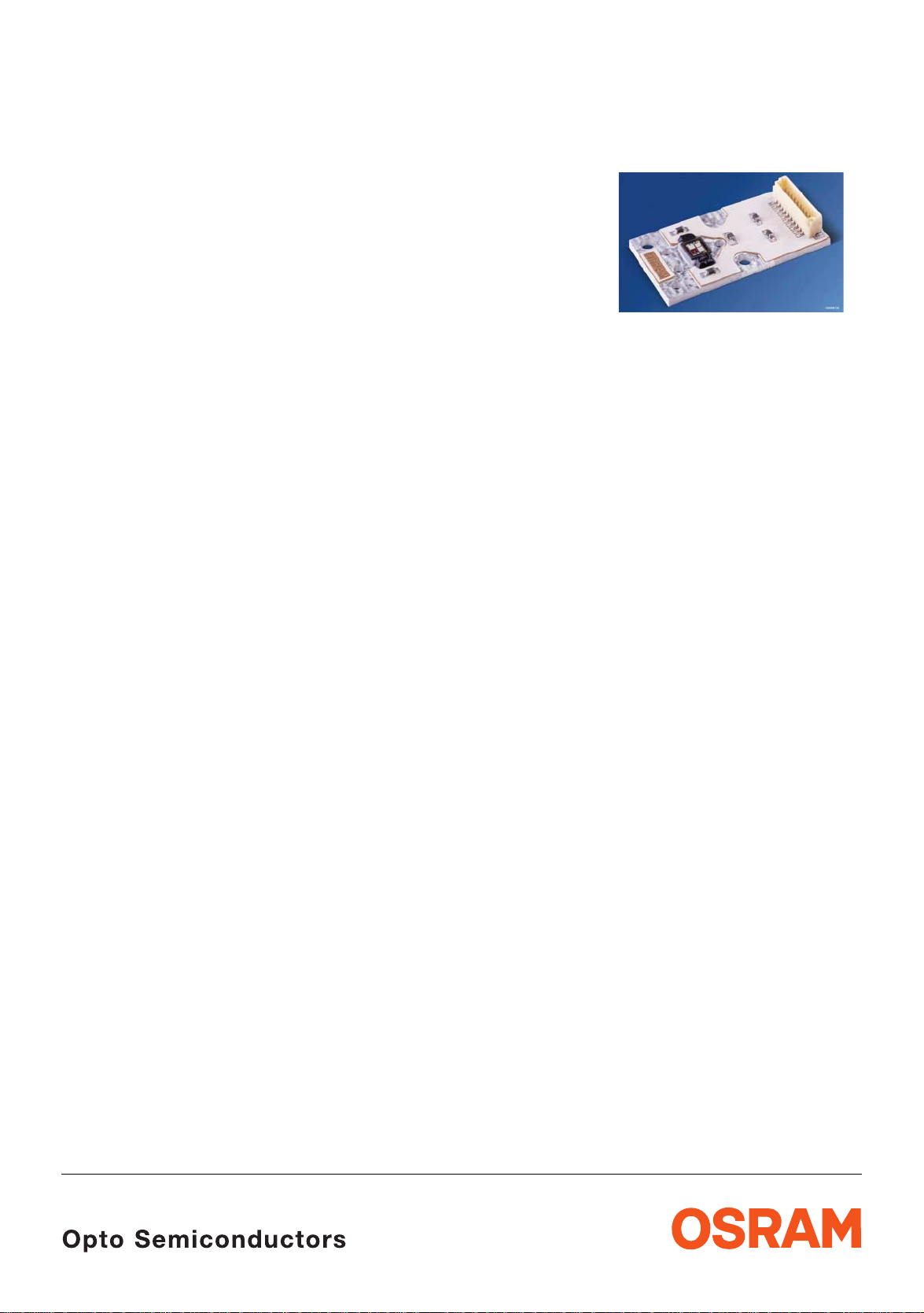
OSTAR - Projection
Lead (Pb) Free Product - RoHS Compliant
LE ATB A2A
Vorläufige Daten / Preliminary Data
Besondere Merkmale
• Gehäusetyp: Kompakte Lichtquelle in
Multi-Chip on Board Technologie;
planvergossen
• Besonderheit des Bauteils: extrem hohe
Helligkeit dank Oberflächenemission und
niedrigem
R
th
Vorbereitet für den Einsatz mit zus. Optik
• Wellenlänge: 617 nm (amber),
525
nm (true green), 464 nm (blau)
• Abstrahlwinkel: Lambertscher Strahler (120°)
• Abstrahlende Fläche: typ. 2.1 x 2.1 mm²
• Technologie: Thinfilm InGaAlP (amber),
®
ThinGaN
(true green, blau)
• Leuchtdichte: 18*106 cd/m² (amber),
6
14*10
cd/m² (true green), 3,5*106 cd/m² (blau)
• max. optischer Wirkungsgrad:
51
lm/W (amber), 86 lm/W (true green),
lm/W (blau) bei 100 mA mit Linse
17
• Montierbarkeit: verschraubbar
• Stecker: 10 Pin JST BM 10B-SRSS-TB
• ESD-Festigkeit: ESD-sicher bis 2 kV nach
JESD22-A114-B
• Verpackungseinheit: 25 St. pro Box
=
Verpackungseinheit
Features
• package: compact lightsource in multi chip on
board technology planar sealed
• feature of the device: outstanding luminance
due to pure surface emission and low R
th
prepared for additional optics
• wavelength: 617 nm (amber),
525
nm (true green), 464 nm (blue)
• viewing angle: Lambertian Emitter (120°)
• light emitting surface: typ. 2.1 x 2.1 mm²
• technology: Thinfilm InGaAlP (amber),
®
ThinGaN
(true green, blue)
• Luminance: 18*106 cd/m² (amber),
6
14*10
cd/m² (true green), 3.5*106 cd/m² (blue)
• max. optical efficiency: 51 lm/W (amber),
86 lm/W (true green), 17 lm/W (blue) at 100
mA with lens
• mounting methode: screw holes
• connector: 10 Pin JST BM 10B-SRSS-TB
• ESD-withstand voltage: up to 2 kV acc. to
JESD22-A114-B
• method of packing: 25 pcs. per tray
=
packing unit
Anwendungen
• Projektoren
• Medizintechnik: Operationslampen
• Mikroskopbeleuchtung
• Scheinwerfer
• Verkehrszeichen
• Hochwertige Blitzlichter
2006-09-27 1
Applications
•projectors
• medical lighting: surgery light
• microscope illumination
• spotlights
• VMS (variable message signs)
• high end strobe light
Bestellinformation Ordering Information
Typ
Emissionsfarbe
Color of Emission
Type
LE ATB A2A
1)
Seite 17
Lichstärke pro Farbe
Luminous Intensity per Color
I
= 750 mA (A) / 500 mA (T, B)
F
Ι
(cd)
V
amber true green blue
min. typ. min. typ. min. typ.
1)
page 17
LE ATB A2A amber
true green (2 Chips)
blue
Typ
Type
Emissionsfarbe
Color of Emission
LE ATB A2A amber
true green (2 Chips)
blue
Bestellinformation Ordering Information
Typ
Type
12 18
Lichtfluss pro Farbe
23
2)3)
Seite 17
28
2
3.5
2)3)
page 17
Luminous Flux per Color
I
= 750 mA (A) / 500 mA (T, B)
F
Φ
(lm)
V
amber true green blue
min. typ. min. typ. min. typ.
(37) (55)
(71)
(86)
(6)
(10.5)
Bestellnummer
Ordering Code
LE ATB A2A Q65110A3646
2006-09-27 2
Grenzwerte Maximum Ratings
LE ATB A2A
Bezeichnung
Parameter
Betriebstemperatur*
Operating temperature range*
Lagertemperatur
Storage temperature range
Sperrschichttemperatur
Junction temperature
Durchlassstrom pro Chip DC
Forward current per chip DC
(T
board
=25°C)
Stoßstrom pro Chip DC
Surge current per chip DC
t ≤ 10 µs, D = 0.1; T
=25°C
A
Sperrspannung pro Chip DC
Reverse voltage per chip DC
(T
board
=25°C)
Sperrstrom
Reverse current
V
= 0.5 V
R
Leistungsaufnahme pro Farbe
Power consumption per Color
(T
board
=25°C)
* Eine Betauung des Moduls muss vermieden werden.
Condensation on the module has to be avoided.
Symbol
Symbol
T
board, op
T
board, stg
T
j
I
F
I
FM
V
R
I
R
P
tot
Werte
Values
amber true
green
blue
Einheit
Unit
– 40 … + 85 °C
– 40 … + 85 °C
125 °C
750 700 mA
2000 2000 2000 mA
0.5 V
10 mA
2.55 6.0 3.0 W
Kennwerte Charakteristics
Bezeichnung
Parameter
Wärmewiderstand des gesamten Moduls
Thermal resistance of the module
Sperrschicht / Bodenplatte
Junction / base plate
2006-09-27 3
Symbol
Symbol
R
th JB
Werte
Values
amber true
green
Einheit
Unit
blue
5
K/W
Kennwerte
Characteristics
(T
board
= 25 °C)
Bezeichnung
Parameter
Symbol
Symbol
Werte
Values
LE ATB A2A
Einheit
Unit
Wellenlänge des emittierten Lichtes (typ.)
Wavelength at peak emission
I
= 750 mA (A) / 500 mA (T, B)
F
4)
Dominantwellenlänge
Dominant wavelength
I
= 750 mA (A) / 500 mA (T, B) (max.)
F
Spektrale Bandbreite bei 50 % Φ
Spectral bandwidth at 50 % Φ
I
= 750 mA (A) / 500 mA (T, B)
F
Abstrahlwinkel bei 50 %
Viewing angle at 50 % Ι
Durchlassspannung
Forward voltage
I
= 750 mA (A) / 500 mA (T, B) (max.)
F
5)
Temperaturkoeffizient von λ
Temperature coefficient of λ
I
= 750 mA (A) / 500 mA (T, B); –10°C ≤ T ≤ 100°C
F
Temperaturkoeffizient von λ
Temperature coefficient of λ
I
= 750 mA (A) / 500 mA (T, B); –10°C ≤ T ≤ 100°C
F
Seite 17
4)
page 17
rel max
rel max
(Vollwinkel) (typ.)
Ι
V
V
5)
Seite 17
page 17
(typ.)
pro Chip (typ.)
peak
per chip
peak
pro Chip (typ.)
dom
per chip
dom
(min.)
(typ.)
(typ.)
(min.)
Temperaturkoeffizient von VF pro Chip (typ.)
Temperature coefficient of VF per chip
I
= 750 mA (A) / 500 mA (T, B); –10°C ≤ T ≤ 100°C
F
Optischer Wirkungsgrad ohne Linse
Optical efficiency without Lens (typ.)
I
= 750 mA (A) / 500 mA (T, B)
F
6)
max. Optischer Wirkungsgrad mit Linse
6)
max. Optical efficiency with Lens
I
= 100 mA (R, T, B)
F
page 17
Seite 17
(typ.)
Abstrahlende Fläche (typ.)
Radiating Surface
λ
λ
λ
λ
peak
dom
dom
dom
amber true
green
627 521 460 nm
613
617
625
517
525
534
blau
458
464
469
∆λ 20 44 24 nm
2
ϕ
V
F
V
F
V
F
TC
TC
TC
η
opt
η
opt max.
A
Color
λpeak
λdom
V
120 120 120 Grad
2.1
2.9
3.4
2.9
3.5
4.0
2.9
3.5
4.0
0.14 0.05 0.05 nm/K
0.08 0.01 0.02 nm/K
– 2.5 – 4.0 – 4.0 mV/K
25
51
1.0 2.0 1.0
25
86
6
17
nm
nm
nm
deg.
V
V
V
lm/W
lm/W
mm²
Leuchtdichte
Luminance (typ.)
I
= 750 mA (A) / 500 mA (T, B)
F
2006-09-27 4
L
V
18*10
6
14*10
6
3.5*10
6
cd/m²
SMD NTC Thermistors SMD NTC Thermistors
LE ATB A2A
R
25
[Ω]
No. of R/T
characteristics*
B
[K]
25/50
B
[K]
25/85
Resistance
Tolerance
∆ RN/R
N
B value
Tolerance
∆ B/B
10k EPCOS 8502 3940 3980 ± 5% ± 3%
* for further information please visit www.epcos.com
1
1
---
------–
T
T
N
R
⎛⎞
B
⋅
⎝⎠
T
R
e
⋅=
N
RT = NTC resistance in Ω at temperature T in K
RN = NTC resistance in Ω at rated temperature TN
in K (T
= 298 K for test condition)
N
T, TN = temperature in K
e = base of the natural logarithm (e = 2.71828)
B = B value, material specific constant of the NTC thermistor
2) 7)
page 17
OHL02609
Seite 17
BB
NT⁄
TT
⋅
N
----------------
TT
–
N
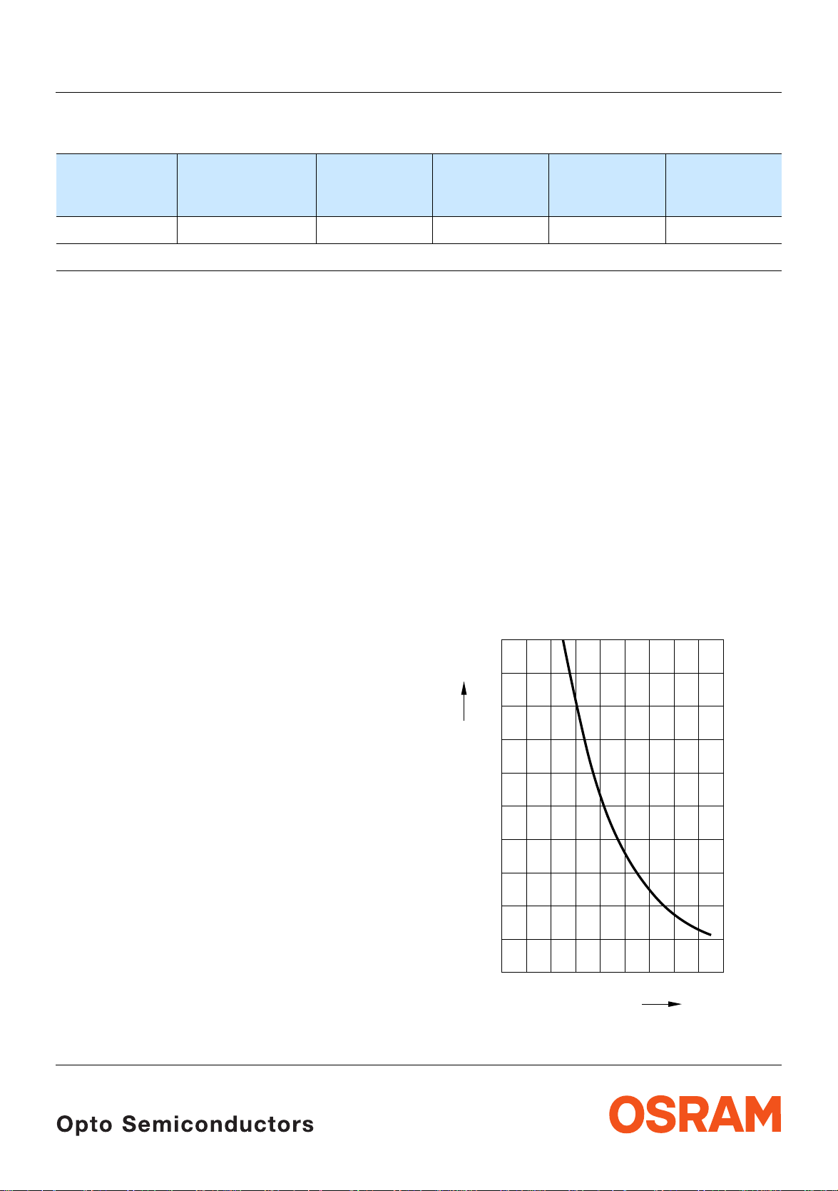
Typische Thermistor Kennlinie
R
N
-------
ln⋅==
R
T
Typical Thermistor Graph
I
= f (VF); T
F
10000
Ω
board
= 25 °C
2) 7)
R
2006-09-27 5
7000
6000
5000
4000
3000
2000
1000
0
0˚C
10 20 30 40 50 60 70 90
T
NTC
2)
Seite 17
Relative spektrale Emission
Relative Spectral Emission
2)
page 17
V(λ) = spektrale Augenempfindlichkeit / Standard eye response curve
Φ
= f (λ), T
rel
Φ
100
rel
= 25 °C, IF = 750 mA (A) / 500 mA (T, B)
board
%
80
60
40
20
V
λ
blue
true green
amber
LE ATB A2A
OHL02471
0
400
Abstrahlcharakteristik2)
Radiation Characteristic
Φ
= f (ϕ); T
rel
50˚
60˚
70˚
80˚
90˚
board
= 25 °C
Seite 17
2)
page 17
550450 500 600
0˚10˚20˚40˚ 30˚
ϕ
1.0
0.8
0.6
0.4
0.2
0
650 nmλ700
OHL01660
100˚
1.0 0.8 0.6 0.4
0˚ 20˚ 40˚ 60˚ 80˚ 100˚ 120˚
2006-09-27 6

LE ATB A2A
2)
Seite 17
Durchlassstrom (amber)
Forward Current (amber)
I
= f (VF); T
F
10
1
board
= 25 °C
2)
page 17
OHL02694
A
I
F
0
10
5
-1
10
5
-2
10
1.5
2.5 3 3.5 4 V 5
2
V
Durchlassstrom / (true green / blau)
Forward Current (true green / blue)
I
= f (VF); T
F
3
A
I
F
board
= 25 °C
OHL02695
F
2)
2)
page 17
Seite 17
) 8)
Seite 17
Relative Lichtstärke
Relative Luminous Intensity
Ι
V/ΙV(750 mA (A) / 500 mA (T, B))
=1ms, D=0,0003
t
P
I
V
I
V (ref. mA)
10
0
) 8)
= f (IF); T
page 17
board
= 25 °C;
OHL02495
5
true green
amber
10
blue
-1
5
-2
10
1
10
Relative Lichtstärke
Relative Luminous Intensity
Ι
V/ΙV(25 °C)
= f (Tj); IF = 750 mA (A) / 500 mA (T, B)
5210
)
Seite 17
)
page 17
1.6
I
V
I
V (25 ˚C)
5
3
mA
10
I
F
OHL03077
0
10
5
-1
10
2
2.5 3 3.5 4 4.5 V 5.5
V
F
2006-09-27 7
1.2
1.0
0.8
amber
true green
blue
0.6
0.4
0.2
0
-40 ˚C-20 0 20 40 60 100
T
j
LE ATB A2A
Dominante Wellenlänge
board
2)
= 25 °C
amber
Dominant Wavelength
LA, λ
λ
dom
dom
= f (IF); T
618.0
nm
617.5
617.0
616.5
616.0
615.5
615.0
0mA
200 400 600 1000
Dominante Wellenlänge
board
2)
= 25 °C
Dominant Wavelength
LB, λ
λ
dom
dom
= f (IF); T
470
nm
2)
Seite 17
page 17
2)
Seite 17
page 17
OHL01659
I
F
OHL01670
Dominante Wellenlänge
board
2)
= 25 °C
true green
Dominant Wavelength
LT, λ
λ
dom
540
dom
535
530
525
520
515
= f (IF); T
nm
0mA
200 400 600 1000
2)
Seite 17
page 17
OHL01671
I
F
468
467
466
blue
465
464
463
462
461
0mA
200 400 600 1000
I
F
2006-09-27 8

LE ATB A2A
Relative Vorwärtsspannung
Relative Forward Voltage
∆VF = VF - V
0.30
V
V
∆
F
0.20
0.15
0.10
0.05
0
-0.05
= f(Tj); IF= 750 mA amber
(25 °C)
F
2)
2)
Seite 17
page 17
OHL02985
Relative Vorwärtsspannung
Relative Forward Voltage
∆VF = VF - V
= f(Tj); IF= 500 mA (blue/true
(25 °C)
F
2)
green)
0.4
V
V
∆
F
0.2
0.1
0
-0.1
-0.2
2)
Seite 17
page 17
OHL02671
-0.10
-60
-40 -20 0 20 ˚C6040
100
T
j
-0.3
-20 0 20 40
-40
˚C60 100-60
T
j
2006-09-27 9

LE ATB A2A
Maximal zulässiger Durchlassstrom
Max. Permissible Forward Current
1 Chip on; I
I
F
= f (TS)
F
1000
mA
800
700
600
blue / true green
amber
500
400
300
200
100
0
02040 ˚C60 80 100
OHL02591
T
Board
Maximal zulässiger Durchlassstrom für 4 Chip
Max. Permissible Forward Current for 4 Chip
(operated parallel;current for single chip is If/4) I
3500
OHL02593
mA
I
F
= f (TS)
F
Maximal zulässiger Durchlassstrom für 2 Chip
Max. Permissible Forward Current for 2 Chip
(operated parallel;current for single chip is If/2) I
2000
OHL02592
mA
I
F
1600
1400
1200
blue / true green
amber
1000
800
600
400
200
0
02040 ˚C60 80 100
T
Board
= f (TS)
F
2500
amber
blue / true green
2000
1500
1000
500
0
02040 ˚C60 80 100
T
Board
2006-09-27 10

LE ATB A2A
Zulässige Impulsbelastbarkeit IF = f (tp)
Permissible Pulse Handling Capability
amber Duty cycle D = parameter, T
board
1 chip operated
2.1
A
I
F
D
2.0
t
P
t
P
=
T
T
1.9
1.8
0.2
1.7
0.3
1.6
0.5
1.5
1.4
0.5 1.5 2.5 3.5 4.5
Zulässige Impulsbelastbarkeit IF = f (tp)
Permissible Pulse Handling Capability
amber Duty cycle D = parameter, T
board
1 chip operated
2.1
A
I
F
D
1.9
1.8
1.7
1.6
1.5
t
P
t
P
=
T
D
T
=
0.005
0.01
0.02
0.05
0.1
0.2
1.4
0.3
0.5
1.3
1.2
= 25 °C
OHL02594
=
D
0.005
0.01
0.02
0.05
0.1
t
p
= 85 °C
OHL02595
Zulässige Impulsbel astbarkeit IF = f (tp)
Permissible Pulse Handling Capability
blue, true green Duty cycle D = parameter, T
board
= 25°C
1 chip operated
2.1
A
I
F
I
F
2.0
t
P
=
D
T
1.9
t
P
OHL02596
T
D
I
F
=
0.005
1.8
0.01
0.02
0.05
1.7
1.6
0.2
0.1
0.3
1.5
0.5
1.4
6ms
1.3
6ms0.5 1.5 2.5 3.5 4.5
t
p
Zulässige Impulsbel astbarkeit IF = f (tp)
Permissible Pulse Handling Capability
blue, true gree n Duty cycle D = parameter, T
board
= 85°C
1 chip operated
2.1
I
F
A
I
F
t
P
=
D
T
1.9
t
P
OHL02597
T
I
F
1.8
D
1.7
1.6
1.5
1.4
=
0.005
0.01
0.02
0.05
0.1
0.2
0.3
1.3
0.5
1.2
1.1
1.1
1.0
0.5 1.5 2.5 3.5 4.5
6ms
t
p
2006-09-27 11
1.0
0.9
6ms0.5 1.5 2.5 3.5 4.5
t
p

LE ATB A2A
Zulässige Impulsbelastbarkeit IF = f (tp)
Permissible Pulse Handling Capability
true green Duty cycle D = parameter, T
2 chips operated parallel; current for single chip is If/2
4.2
A
I
F
4.0
D
t
t
P
=
T
board
P
T
= 25°C
OHL02600
I
F
3.8
=
D
3.6
0.005
0.01
3.4
3.2
0.02
0.05
0.1
0.2
3.0
0.3
2.8
2.6
2.4
0.5 1.5 2.5 3.5 4.5 6ms
0.5
t
p
Zulässige Impulsbel astbarkeit IF = f (tp)
Permissible Pulse Handling Capability
true green Duty cycle D = parameter, T
2 chips operated parallel; current for single chip is If/2
4.2
A
I
F
D
3.8
t
t
P
=
T
3.6
3.4
3.2
3.0
board
P
T
D
=
0.005
0.01
0.02
0.05
= 85°C
OHL02601
I
F
0.1
2.8
2.6
0.2
0.3
0.5
2.4
2.2
2.0
1.8
1.6
0.5 1.5 2.5 3.5 4.5 6ms
t
p
2006-09-27 12
Maßzeichnung
9)
Package Outlines
Seite 17
9)
page 17
LE ATB A2A
Chip-Position:
1: Blue
2: Green 1
3: Green 2
4: Amber
Pin-Assignment:
a1: Cathode G1
2: Anode G1
3: Anode B
4: Cathode B
5: NTC
6: NTC
7: Cathode G2
8: Anode G2
9: Anode R
10: Cathode R
Kathodenkennung: Markierung
Cathode mark: mark
Gewicht / Approx. weight: 2 g
Verwendeter Stecker / Used male connector on board: J ST BM 10B-SR SS-TB (www.jst.com)
Empfohlene Gegenstecker / JST SHR-10V-S (www.jst.com)
Recommended female connector for power supply: JST SHR-10V-S-B (www.jst.com)
Kontakt - Pins: SSH-003T-P0.2 (www.jst.com)
2006-09-27 13

Ersatzschaltbild für den thermischen Widerstand
2)
Analogon lay out for thermal resistance
page 17
2)
Seite 17
LE ATB A2A
T
Baseplate
Verpackung
Method of Packing
=
9)
Seite 17
T
Ambient
9)
page 17
R
th,board
= 3 K/W
Board
R
th,chip
= 8 K/W
Chip 1
Chip 2
T
Submount
Chip 3
Chip 4
25 St. pro Box = Verpackungseinheit
25 pcs. per tray = packing unit
T
Junction,chip1
T
Junction,chip2
T
Junction,chip3
T
Junction,chip4
OHTE2881
2006-09-27 14

Barcode-Tray-Etikett (BTL) Barcode-Tray-Label (BTL)
LE ATB A2A
Data
Matrix
Code
BIn Nr.
BIN
LE xxx xxx
MATERIAL:
Kartonverpackung und Materialien Transportation Packing and Materials
Box
Group:
xxxx-xxxx-xxxx Date Code
Bar Code
Material Number Batch Batch Number
DC:
OHA02684
2006-09-27 15
Barcode label
0
2
0
1
2
-
-
P
1
-
:
1
Q
T
n
:
i
S
2
B
n
:
p
i
R
3
B
m
n
Y
i
C
6
e
R
M
B
T
T
7
0
C
E
2
R
6
T
D
2
L
D
0
T
C
X
4
M
E
2
E
0
L
Y
6
T
2
l
2
8
P
S
a
a
2
1
n
L
O
1
o
i
R
-
3
T
t
i
:
i
d
Q
R
d
lt
7
A
+
A
7
V
u
1
0
-
K
R
M
C
P
A
:
P
P
U
O
R
G
)
G
(
4
4
1
0
to
:
s
C
p
/
D
)
O
D
9
uctor
M
(
d
0
0
210021998
on
:
RA
0
4
O
2
3
ic
S
:
N
2
Y
O
1
H
T
em
C
H
Q
S
T
)
A
G
Q
(
B
3
)
2
P
1
6
:
(
O
245
N
T
1
Muster
O
L
0
)
0
T
1
11
(
:
O
N
D
O
R
P
)
X
(
Original packing label
OHA02886

LE ATB A2A
Revision History: 2006-09-27
Previous Version: 2006-09-13
Page Subjects (major changes since last revision) Date of change
8 Relative Forward Voltage 2006-08-08
Anm.: Gemäß IEC 60825-1 (EN 60825-1) gilt für amber, true green:
Note: According IEC 60825-1 (EN 60825-1) for amber, true green:
LED RADIATION
DO NOT VIEW DIRECTLY
WITH OPTICAL INSTRUMENTS
CLASS 1M LED PRODUCT
NICHT DIREKT MIT OPTISCHEN
INSTRUMENTEN BETRACHTEN
OHW02884
LED STRAHLUNG
LED KLASSE 1M
OHW12884
Anm.: Gemäß IEC 60825-1 (EN 60825-1) gilt für blau:
Note: According IEC 60825-1 (EN 60825-1) for blue:
LED RADIATION
LED STRAHLUNG
NICHT DIREKT IN
DO NOT STARE INTO BEAM
DEN STRAHL BLICKEN
CLASS 2 LED PRODUCT
OHW02885
Attention please!
The information describes the type of component and sha ll not be c ons idered as assured characteris tics .
Terms of delivery and rights to change design reserved. Due to technical requirements components may contain
dangerous substances. For information on the types in question please contact our Sales Organization.
If printed or downloaded, please find the latest version in the Inte rnet .
Packing
Please use the recycling operators k nown to you . We can als o help you – get in touch wit h your near est sales offic e.
By agreement we will take p acking material back, if it is sorted. You m ust bear the costs of transport. For packing
material that is returned to us unsorted or which we are not obliged to accept, we shall have to invoice you for any costs
incurred.
Components used in life-support devices or systems must be expressly authorized for such purpose! Critical
components
OSRAM OS.
10)
page 17
may only be used in life-support devices or systems
11)
LED KLASSE 2
page 17
with the express written approval of
OHW12885
2006-09-27 16

LE ATB A2A
Fußnoten:
1)
Helligkeitswerte werden mit einer Stromeinprägedauer
ms und einer Genauigkeit von ± 11% ermittelt.
von 25
Messbedingung für Lichtstärkemessung nach CIE127
Condition A.
2)
Wegen der besonderen Prozessbedingungen bei der
Herstellung von LED können typische oder abgeleitete
technische Parameter nur aufgrund statistischer Werte
wiedergegeben werden. Diese stimmen nicht
notwendigerweise mit den Werten jedes einzelnen
Produktes überein, dessen Werte sich von typischen
und abgeleiteten Werten oder typischen Kennlinien
unterscheiden können. Falls erforderlich, z.B. aufgrund
technischer Verbesserungen, werden diese typischen
Werte ohne weitere Ankündigung geändert.
3)
Min. ΦV Werte werden aus den Iv - Werten berechnet.
Die Helligkeitswerte auf Seite 2 wurden ohne
Primäroptik gemessen.
4)
Wellenlängen werden mit einer Stromeinprägedauer
von 25 ms und einer Genauigkeit von ±1
5)
Spannungswerte werden mit einer Stromeinprägedauer
ms und einer Genauigkeit von ±0,1 V ermittelt.
von 1
6)
Für den Fall, dass eine Optik wie z. B. eine
nm ermittelt.
Halbsphärenlinse als Primäroptik verwendet wird, kann
der Lichtfluss bis zu 40% für rot und grün und 36% für
blau erhöht werden.
7)
Die R-T-Kurve eines NTC läßt sich in einem engen
Bereich um den spezifizierten Wert herum in erster
Näherung durch einen exponentialen Zusammenhang
beschreiben. Sofern eine detailliertere Beschreibung
der R-T-Kurve für die Praxis nötig ist, können eine
ganauere Formel und entsprechende tabellierte Werte
bei EPCOS gefunden werden.
8)
Im gestrichelten Bereich der Kennlinien muss mit
erhöhten Helligkeitsunterschieden zwischen
Leuchtdioden innerhalb einer Verpackungseinheit
gerechnet werden.
9)
Maße werden wie folgt angegeben: mm (inch).
10)
Ein kritisches Bauteil ist ein Bauteil, das in
lebenserhaltenden Apparaten oder Systemen
eingesetzt wird und dessen Defekt voraussichtlich zu
einer Fehlfunktion dieses lebenserhaltenden Apparates
oder Systems führen wird oder die Sicherheit oder
Effektivität dieses Apparates oder Systems
beeinträchtigt.
11)
Lebenserhaltende Apparate oder Systeme sind für (a)
die Implantierung in den menschlichen Körper
oder
(b) für die Lebenserhaltung bestimmt.
Falls sie versagen, kann davon ausgegangen werden,
dass die Gesundheit und das Leben des Patienten in
Gefahr ist.
Remarks:
1)
Brightness groups are tested at a current pulse duration
ms and a tolerance of ± 11%. Condition for
of 25
luminous intensity measurement acc. to CIE127
condition A
2)
Due to the special conditions of the manufacturing
processes of LED, the typical data or calculated
correlations of technical parameters can only reflect
statistical figures. These do not necessarily correspond
to the actual parameters of each single product, w hich
could differ from the typical data and calculated
correlations or the typical characeristic line.
If requested, e.g. because of technical improvements,
these typ. data will be changed without any further
notice.
3)
Min. ΦV values are calculated from Iv values.
Brightness values stated on page 2 are measured
without primary optics.
4)
Wavelengths are tested at a current pulse duration of 25
ms and a tolerance of ±1
5)
Forward voltages are tested at a current pulse duration
ms and a tolerance of ±0.1 V.
of 1
6)
If an optic, such as a hemispherical lens is added, the
nm.
luminous flux values can be increased up to 40% for red
and green and 36% for blue.
7)
The R-T-Curve of an NTC thermistor can be roughly
described in a restricted range around the rated
temperautre. If a more precise desciption of the R/T
curve is required for practical applications a refined
formular and the corresponding tabulated values can be
found at EPCOS
8)
In the range where the line of the graph is broken, you
must expect higher brightness differences between
single LEDs within one packing unit.
9)
Dimensions are specified as follows: mm (inch).
10)
A critical component is a component used in a
life-support device or system whose failure can
reasonably be expected to cause the failure of that
life-support device or system, or to affect its safety or the
effectiveness of that device or system.
11)
Life support devices or systems are intended
(a) to be implanted in the human body,
or
(b) to support and/or maintain and sustain human life. If
they fail, it is reasonable to assume that the health and
the life of the user may be endangered.
Published by
OSRAM Opto Semiconductors GmbH
Wernerwerkstrasse 2, D-93049 Regensburg
www.osram-os.com
© All Rights Reserved.
2006-09-27 17
 Loading...