


Hyper Multi TOPLED
®
Enhanced optical Power LED (HOP2000 / ATON®)
LATB T66B
Vorläufige Daten / Preliminary Data
Besondere Merkma le
• Gehäusetyp: weißes P-LCC-4 Gehäuse;
Kontrasterhöhung durch schwarze Oberfläche
(RGB-Displays) und diffuses Harz
• Besonderheit des Bauteils: additive
Farbmischung durch unabhängige Ansteuerung
aller Chips
• Wellenlänge: 617 nm (amber),
528 nm (true green), 470 nm (bl au)
• Abstrahlwinkel: Lambertscher Strahler (120°)
• Technologie: InGaAlP (amber),
InGaN (true green, blau)
• optischer Wirkungsgrad: 24 lm/W (amber),
13 lm/W (true green), 3 lm/W (blau)
• Gruppierungsparameter: Lichtstärke
• Verarbeitungsmethode: für alle
SMT-Bestücktechniken geeignet
• Lötmethode: IR Reflow Löten und
Wellenlöten (TTW)
• Vorbehandlung: nach JEDEC Level 2
• Gurtung: 8 mm Gurt mit 2000/Rolle, ø180 mm
oder 8000/Rolle, ø330 mm
• ESD-Festigkeit: ESD-sicher bis 2 kV nach
EOS/ESD-5.1-1993
Features
• package: white P-LCC-4 package;
higher contrast by a black surface
(RGB-Displays) and diffused resin
• feature of the device: additive mixture of color
stimuli by independent driving of each chip
• wavelength: 617 nm (amber),
528 nm (true green), 470 nm (blu e)
• viewing angle: Lamberti an Em itter (120°)
• technology: InGaAlP (amber),
InGaN (true green, blue)
• optical efficiency: 24 lm /W (amber),
13 lm/W (true green) , 3 lm/W (blue)
• grouping parameter: luminous intensity
• assembly methods: suitable for all
SMT assembly methods
• soldering methods: IR reflow soldering and
TTW soldering
• preconditioning: acc. to JEDEC Level 2
• taping: 8 mm tape with 2000/r eel, ø180 mm
or 8000/reel, ø330 mm
• ESD-withstand voltage: up to 2 kV acc. to
EOS/ESD-5.1-1993
Anwendungen
• Anzeigen im Innen- und Außenbereich
(z.B. im Verkehrsbereich; Lauf schr iftanzeigen)
• Leuchtdiodenchips getrennt ansteuerbar
• Vollfarbdisplays bzw. RGB-Displays
• Hinterleuchtung (LCD, Schalter, Tasten,
Displays, Werbebeleuchtung,
Allgemeinbeleuchtung)
• Einkopplung in Lichtleiter
2002-05-24 1
Applications
• indoor and outdoor displays (e.g. displays for
traffic; light writing display s)
• LED chips can be controlled separately
• full color displays, RGB-Displays
• backlighting (LCD, switches, keys, displays,
illuminated advertising, general lighting)
• coupling into light guides
LATB T66B
Typ
Emissionsfarbe
Type
Color of
Emission
LATB T66B amber
true green
blue
Bestell - Information
Ordering Information
Typ
Type
LATB T66B-ST-1+ST-78+PQ-1
LATB T66B-ST-1+ST-7+PQ-1
LATB T66B-ST-1+ST-8+PQ-1
Farbe der
Lichtaustrittsfläche
Color of the
Light Emitting
Area
colorless diffused
and
black painted
package surface
Lichtstärke
Luminous Intensity
I
= 20 mA
F
I
(mcd)
V
amber true green blue
180 ...450 180 ...450 45 ... 112
Bestellnummer
Ordering Code
Q65110-A0152
Q65110-A0181
Q65110-A0182
Anm.: -78 gesamter Farbbereich, Lieferung in Einzelgruppen (siehe Seite 5)
Die Standardlieferform von Serientypen beinhaltet eine Familiengruppe. Einzelne Gruppen sind
nicht erhältlich.
In einer Verpackungseinheit / Gurt ist immer nur eine Gruppe pro Farbe enthalten.
Dimmverhältnis im Gleichstrom-Betrieb max. 5:1 für amber
Note: -78 Total color tolerance range, delivery in single groups (please see page 5)
The standard shipping format for serial types includes a family group. Individual groups are not
available.
No packing unit / tape ever contains more than one luminous intensity group per color.
Dimming range for direct current mode max. 5:1 for amber
2002-05-24 2
Grenzwerte
Maximum Ratings
LATB T66B
Bezeichnung
Parameter
Betriebstemperatur
Operating temperature range
Lagertemperatur
Storage temperature range
Sperrschichttemperatur
Junction temperature
Durchlassstrom
Forward current
Stoßstrom
Surge current
t
= 10 µs, D = 0.005
p
Sperrspannung
Reverse voltage
Leistungsaufnahme
Power consumption
Symbol
Symbol
T
op
T
stg
T
j
I
F
I
FM
V
R
P
tot
Werte
Values
Einheit
Unit
LA LT LB
– 40 … + 100 °C
– 40 … + 100 °C
+ 125 + 125 + 110 °C
70 30 30 mA
0.10 0.25 0.20 A
555V
180 140 140 mW
Wärmewiderstand
Thermal resistance
Sperrschicht/Umgebung 1 chip on
Junction/ambient 3 chips on
Sperrschicht/Lötpad 1 chip on
Junction/solder point 3 chips on
Montage auf PC-Board FR 4 (Padgröße
mounted on PC board FR 4 (pad size
≥ 16 mm
≥ 16 mm
2
R
th JA
R
th JA
R
th JS
R
th JS
2
)
480
770
260
420
530
820
310
470
530
820
310
470
K/W
K/W
K/W
K/W
)
2002-05-24 3
Kennwerte (TA = 25 °C)
Characteristics
LATB T66B
Bezeichnung
Parameter
Symbol
Symbol
Werte
Values
Einheit
Unit
LA LT LB
Wellenlänge des emittierten Lichtes (typ.)
λ
peak
628 523 465 nm
Wavelength at peak emission
I
= 20 mA
F
Dominantwellenlänge
Dominant wavelength
I
= 20 mA
F
Spektrale Bandbreite bei 50 %
Spectral bandwidth at 50 %
I
= 20 mA
F
Abstrahlwinkel bei 50 %
Viewing angle at 50 %
Durchlassspannung
Forward voltage (typ.)
I
= 20 mA (max.)
F
Sperrstrom (typ.)
Reverse current (max.)
V
= 5 V
R
Temperaturkoeffizient von
Temperature coefficient of
I
=20 mA; –10°C ≤ T ≤ 100°C
F
Temperaturkoeffizient von
Temperature coefficient of
I
= 20 mA; –10°C ≤ T ≤ 100°C
F
Temperaturkoeffizient von
Temperature coefficient of
I
= 20 mA; –10°C ≤ T ≤ 100°C
F
Optischer Wirkungsgrad (typ.)
1)
I
rel max
I
rel max
I
(Vollwinkel) (typ.)
V
I
V
2)
λ
peak
λ
peak
λ
dom
λ
dom
V
F
V
F
(typ.)
(typ.)
(min.)
(typ.)
(typ.)
(typ.)
λ
dom
617
–2 / +7
528
± 9
470
± 6
nm
∆λ 16 33 25 nm
2ϕ 120 120 120 Grad
deg.
V
V
V
I
R
I
R
TC
TC
TC
η
opt
F
F
F
λpeak
λdom
V
2.0
2.4
0.01
10
3.5
4.3
0.01
10
3.8
4.3
0.01
10
0.13 0.04 0.05 nm/K
0.06 0.03 0.04 nm/K
– 1.8 – 3.6 – 3.1 mV/K
24 13 3 lm/W
V
V
V
µA
µA
Optical efficiency
I
= 20 mA
F
1)
Wellenlängen werden m it einer St romeinprägedauer von 25 ms und einer Genauigkeit von ±1 nm ermittelt.
Wavelengths are tested at a current pulse duration of 25 ms and a tolerance of ± 1 nm.
2)
Spannungswerte werde n mit einer Stromeinprägedau er von 1 ms und einer Genauigkeit von ±0,1 V ermittelt.
Voltages are tested at a curre nt puls e duration of 1 ms and a tolerance of ±0.1 V.
2002-05-24 4
1)
Wellenlängengruppen / Wavelength groups
LATB T66B
Gruppe
Group
true green Einheit
min. max.
Unit
7 519 528 nm
8 528 537 nm
Lichtgruppe
Luminous
Intensity
Lichtstärke
Luminous
Intensity
Group
I
(mcd)
V
S+S+P
S+S+Q
S+T+P
S+T+Q
T+S+P
T+S+Q
T+T+P
T+T+Q
180 ...280
180 ...280
180 ...280
180 ...280
280 ...450
280 ...450
280 ...450
280 ...450
Lichtstrom
Luminous
Flux
Φ
(mlm)
V
Lichtstärke
Luminous
Intensity
I
(mcd)
V
Lichtstrom
Luminous
Flux
Φ
(mlm)
V
Lichtstärke
Luminous
Intensity
I
(mcd)
V
amber true green blue
680 (typ.)
680 (typ.)
680 (typ.)
680 (typ.)
1075 (typ.)
1075 (typ.)
1075 (typ.)
1075 (typ.)
180 ...280
180 ...280
280 ...450
280 ...450
180 ...280
180 ...280
280 ...450
280 ...450
680 (typ.)
680 (typ.)
1075 (typ.)
1075 (typ.)
680 (typ.)
680 (typ.)
1075 (typ.)
1075 (typ.)
45 ... 71
71 ... 112
45 ... 71
71 ... 112
45 ... 71
71 ... 112
45 ... 71
71 ... 112
Lichtstrom
Luminous
Flux
Φ
(mlm)
V
95 (typ.)
270 (typ.)
95 (typ.)
270 (typ.)
95 (typ.)
270 (typ.)
95 (typ.)
270 (typ.)
Helligkeitswerte werden m it einer Stromeinprägedauer von 25 ms und einer Genauigkeit von ±11 % ermittelt.
Luminous intensity is tested at a current pulse duration of 25 ms and a tolerance of ±11 %.
Gruppenbezeichnung auf Etikett
Group Name on Label
Beispiel: T-1+S-7+P-1
Example: T-1+S-7+P-1
Lichtgruppe
Luminous
Intensity
Group
(amber)
Wellenlänge
(keine
Gruppierung)
Wavelength
(no grouping)
(amber)
Lichtgruppe
Luminous
Intensity
Group
(true green)
Wellenlänge
Wavelength
(true green)
Lichtgruppe
Luminous
Intensity
Group
(blue)
Wellenlänge
(keine
Gruppierung)
Wavelength
(no grouping)
(blue)
T1S7P1
2002-05-24 5
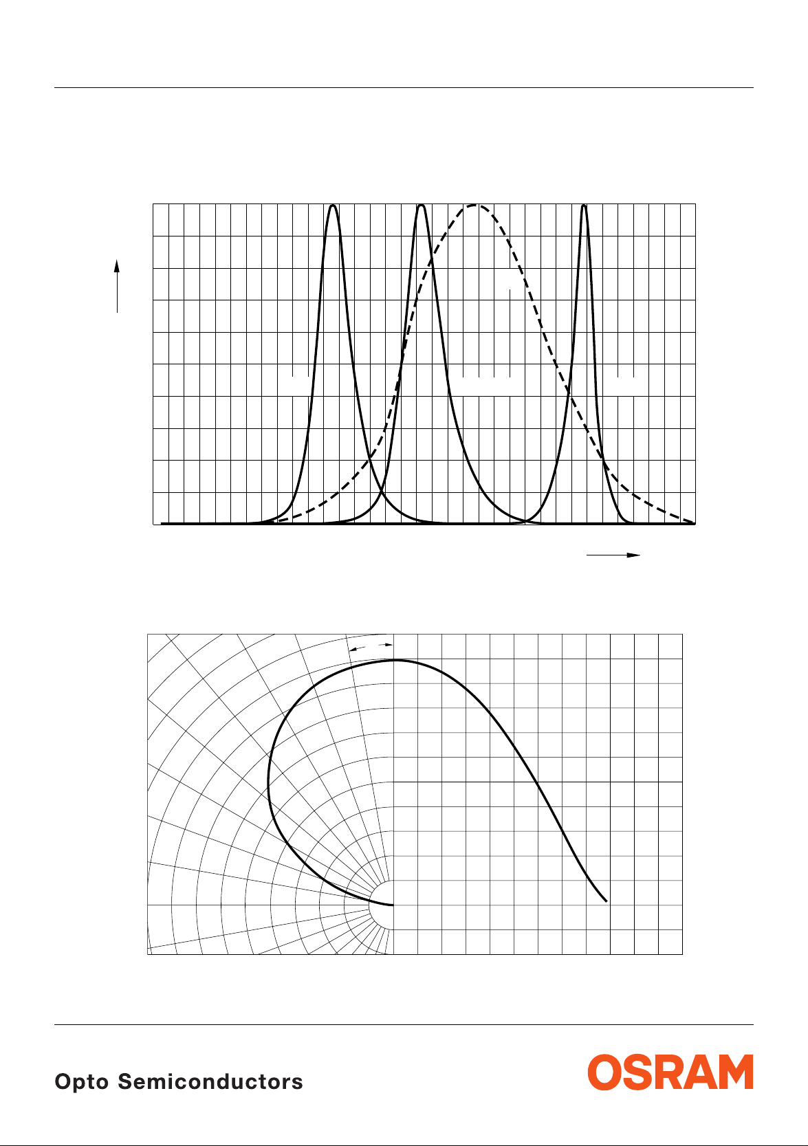
LATB T66B
Relative spektrale Emission I
rel
Relative Spectral Emission
λ) = spektrale Augenempfindlichkeit
V(
Standard eye response curve
100
%
I
rel
80
60
40
20
= f (λ), TA = 25 °C, IF = 20 mA
blue
true green
OHL01452
V
λ
amber
0
350
Abstrahlcharakteristik
Radiation Characteristic
50˚
60˚
70˚
80˚
90˚
400 450 500 550 600 650 700
nm
λ
I
= f (ϕ)
rel
0˚10˚20˚40˚ 30˚
ϕ
1.0
0.8
0.6
0.4
0.2
0
OHL01660
100˚
1.0 0.8 0.6 0.4
2002-05-24 6
0˚ 20˚ 40˚ 60˚ 80˚ 100˚ 120˚
LATB T66B
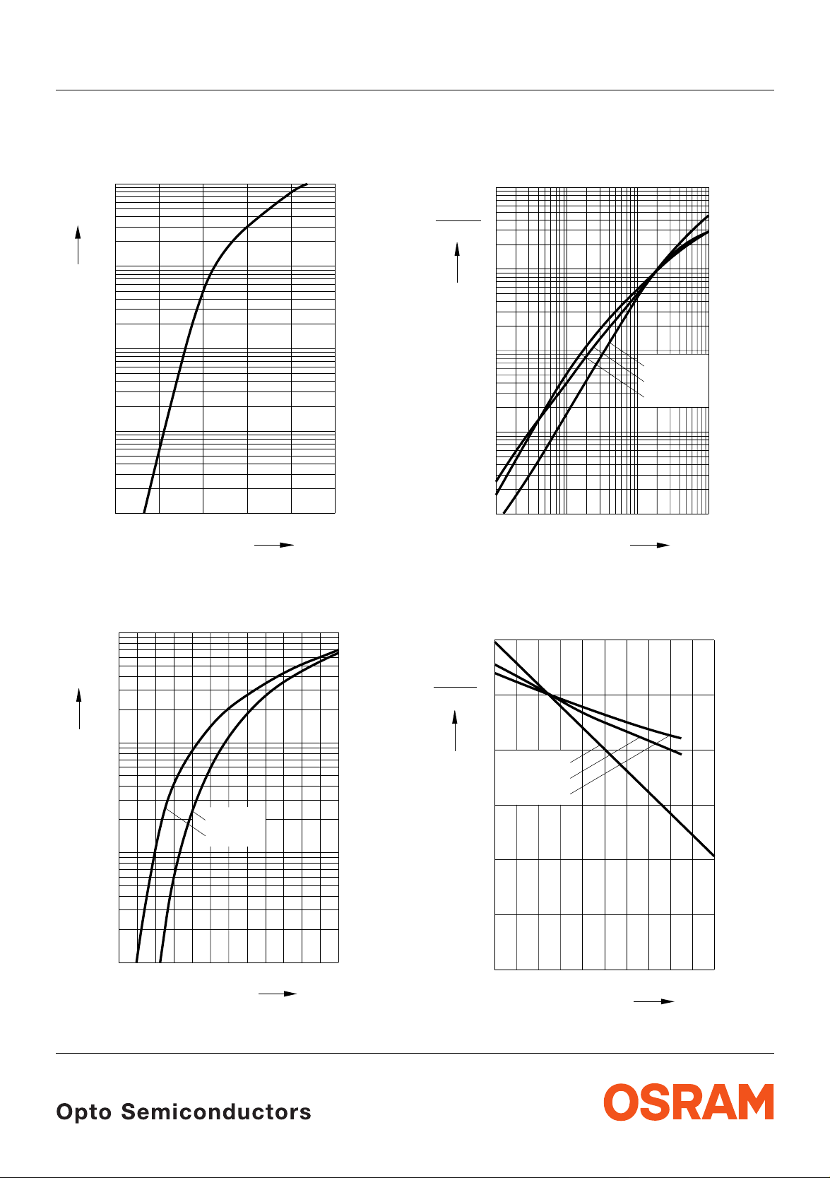
Durchlassstrom IF = f (VF)
Forward Current
T
= 25 °C
A
2
10
mA
I
F
1
10
5
0
10
5
-1
10
5
-2
10
1.4
Durchlassstrom
Forward Current
T
= 25 °C
A
2
10
mA
5
I
F
1.6 1.8 2.0 2.2 2.4
I
= f (VF)
F
OHL00444
V
V
F
OHL01481
Relative Lichtstärke
I
V/IV(20 mA)
Relative Luminous Intensity
T
= 25 °C
A
1
10
I
V
I
(20 mA)
V
0
10
5
-1
10
5
-2
10
5
-3
10
-1 0
10
Relative Lichtstärke
10 10
55
I
V/IV(25 °C)
Relative Luminous Intensity
I
= 20 mA
F
1.2
I
V
I
V
(25 ˚C)
= f (IF)
OHL01473
blue
amber
true green
12
mA
10
I
F
= f (TA)
OHL01477
1
10
5
blue
true green
10
0
5
-1
10
2002-05-24 7
3.5232.5 5V4.54
V
F
0.8
amber
true green
blue
0.6
0.4
0.2
0
020406080
100˚C
T
A

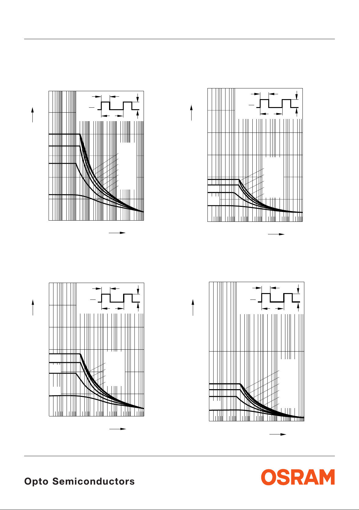
LATB T66B
Maximal zulässiger Durchlassstrom IF = f (T)
Max. Permissible Forward Current
1 chip on
80
mA
I
F
70
60
50
40
30
20
10
0
020 6040
amber
blue
true
green
T
temp. ambient
A
OHL01612
˚C
80
100
T
I
Maximal zulässiger Durchlassstrom
= f (T)
F
Max. Permissible Forward Current
1 chip on
80
mA
I
F
70
amber
OHL01610
Maximal zulässiger Durchlassstrom
Max. Permissible Forward Current
3 chips on
80
mA
I
F
70
60
50
40
30
20
10
0
020 6040
amber
T
temp. ambient
A
true
green
blue
OHL01609
˚C
80
T
Maximal zulässiger Durchlassstrom
Max. Permissible Forward Current
3 chips on
80
mA
I
F
70
OHL01607
I
100
I
F
F
= f (T)
= f (T)
60
50
40
30
blue
20
true
green
10
temp. solder point
T
S
0
020 6040
80
˚C
100
T
2002-05-24 8
60
50
40
30
20
10
temp. solder point
T
S
0
020 6040
amber
true
green
blue
80
100
˚C
T

LATB T66B
Zulässige Impulsbelastbarkeit IF = f (tp)
Permissible Pulse Handling Capability
Duty cycle
D = parameter, T
= 25 °C
A
amber (1 Chip on)
0.5
OHL01505
s
t
p
10
I
F
0.12
A
0.1
0.005
0.08
0.06
0.04
0.02
0
-510-410-310-210-1100101102
0.05
I
Zulässige Impulsbelastbarkeit
= f (tp)
F
Permissible Pulse Handling Capability
Duty cycle
D = parameter, T
= 85 °C
A
amber (1Chip on)
OHL01604
10
s
t
p
I
F
0.12
A
0.10
0.08
0.06
0.04
0.02
0
-510-410-310-210-1100101102
0.005
0.05
0.5
Zulässige Impulsbelastbarkeit IF = f (tp)
Permissible Pulse Handling Capability
Duty cycle
D = parameter, T
= 25 °C
A
amber (3 Chips on)
0.5
OHL00193
10
s
t
p
0.12
A
I
F
0.10
0.08
0.06
0.04
0.02
0
-510-410-310-210-1100101102
0.005
0.05
Zulässige Impulsbelastbarkeit IF = f (tp)
Permissible Pulse Handling Capability
Duty cycle
D = parameter, T
= 85 °C
A
amber (3 Chips on)
OHL01606
10
s
t
p
I
F
0.12
A
0.10
0.08
0.06
0.04
0.005
0.05
0.02
0
-510-410-310-210-1100101102
0.5
2002-05-24 9

LATB T66B
Zulässige Impulsbelastbarkeit IF = f (tp)
Permissible Pulse Handling Capability
Duty cycle
D = parameter, T
= 25 °C
A
true green (1 Chip on)
OHL01400
D
=
0.005
0.01
0.02
0.05
0.1
0.2
0.5
0
t
p
s10110
I
0.30
F
0.25
0.20
0.15
0.10
0.05
A
0
-5 -4 -3
10 10
10 10-210-110
I
Zulässige Impulsbelastbarkeit
= f (tp)
F
Permissible Pulse Handling Capability
Duty cycle
D = parameter, T
= 85 °C
A
true green (1 Chip on)
T
OHL01584
D =
0.005
0.01
0.02
0.05
1
t
p
I
F
2
10s
0.30
t
I
F
0.25
A
=
D
P
t
P
T
0.20
0.15
0.1
0.10
0.2
0.5
0.05
0
2
-5
10
10-410-310-210-110010
Zulässige Impulsbelastbarkeit IF = f (tp)
Permissible Pulse Handling Capability
Duty cycle
D = parameter, T
= 25 °C
A
true green (3 Chips on)
T
D =
0.005
0.01
0.02
0.05
OHL01586
I
F
1
10s
t
p
I
0.30
F
0.25
0.20
0.15
0.10
0.05
A
0.1
0.2
0.5
0
-5
10
10-410-310-210-110010
t
P
=
D
T
t
P
Zulässige Impulsbelastbarkeit IF = f (tp)
Permissible Pulse Handling Capability
Duty cycle
D = parameter, T
= 85 °C
A
true green (3 Chips on)
OHL01575
I
F
I
0.10
F
t
A
=
D
P
t
P
T
T
0.05
D =
0.005
0.1
0.2
0.5
2
0
-5
10
10-410-310-210-110010
0.01
0.02
0.05
1
2
10s
t
p
2002-05-24 10
LATB T66B
Zulässige Impulsbelastbarkeit IF = f (tp)
Permissible Pulse Handling Capability
Duty cycle
D = parameter, T
= 25 °C
A
blue (1 Chip on)
OHL01405
P
I
F
T
D
=
0.005
0.01
0.02
0.05
0.1
0.2
0.5
0
s10110
t
p
I
0.30
F
0.25
0.20
0.15
0.10
0.05
A
0
-5 -4 -3
10 10
t
t
P
D
=
T
10 10-210-110
I
Zulässige Impulsbelastbarkeit
= f (tp)
F
Permissible Pulse Handling Capability
Duty cycle
D = parameter, T
= 85 °C
A
blue (1 Chip on)
T
D =
0.005
0.01
0.02
0.05
0.1
OHL01579
I
F
1
10s
t
p
2
0.30
t
I
F
0.25
A
=
D
P
t
P
T
0.20
0.15
0.10
0.2
0.05
0.5
2
0
-5
10
10-410-310-210-110010
Zulässige Impulsbelastbarkeit IF = f (tp)
Permissible Pulse Handling Capability
Duty cycle
D = parameter, T
= 25 °C
A
blue (3 Chips on)
T
D =
0.005
0.01
0.02
0.05
OHL01576
I
F
1
10s
t
p
I
0.30
F
0.25
0.20
0.15
0.10
0.05
A
t
P
=
D
T
0.1
0.2
0.5
0
-5
10
10-410-310-210-110010
t
P
Zulässige Impulsbelastbarkeit IF = f (tp)
Permissible Pulse Handling Capability
Duty cycle
D = parameter, T
= 85 °C
A
blue (3 Chips on)
OHL01577
P
I
F
I
0.10
F
A
D
t
t
P
=
T
T
0.05
D =
0.005
0.01
0.02
0.05
0.1
0.5
2
0
-5
10
10-410-310-210-110010
0.2
1
2
10s
t
p
2002-05-24 11

LATB T66B
0.9
0.8
0.7
0.6
0.5
0.4
0.3
0.2
0.1
OHA02290
520
530
540
550
560
a)
+
0
0
0.1 0.2 0.3 0.4 0.5 0.6 0.7 0.8 0.9
570
580
590
600
610
620
630
Die Farbkoordinaten des Mischlichtes können innerhalb des mit a) gekennzeichneten Bereichs des Farbdreiecks
erwartet werden.Der Unbuntpunkt (x = 0,33, y = 0,33) ist mit „+“ gekennzeich net .
The color coordinates of the mixed light can be expected wit hin the area of the color triangle marke d a).
The achromatic point (x = 0.33, y = 0.33) is marke d „+“.
2002-05-24 12

Maßzeichnung
Package Outlines
3.0 (0.118)
2.6 (0.102)
2.3 (0.091)
2.1 (0.083)
23
3.0 (0.118)
3.4 (0.134)
0.8 (0.031)
0.6 (0.024)
(2.4 (0.094))
4˚±1
0.1 (0.004) typ
3.3 (0.130)
3.7 (0.146)
LATB T66B
2.1 (0.083)
1.7 (0.067)
0.9 (0.035)
0.7 (0.028)
14
Package marking
0.5 (0.020)
1.1 (0.043)
0.18 (0.007)
0.6 (0.024)
0.4 (0.016)
GPLY6900
1 Cathode Amber (A)
2 Anode A, T, B
3 Cathode Blue (B)
4 Cathode True Green (T)
Maße werden wie folgt angegeb en: m m (inch) / Dimensions are specified as follows: mm (inch).
Gewicht / Approx. weight: 34 mg
2002-05-24 13
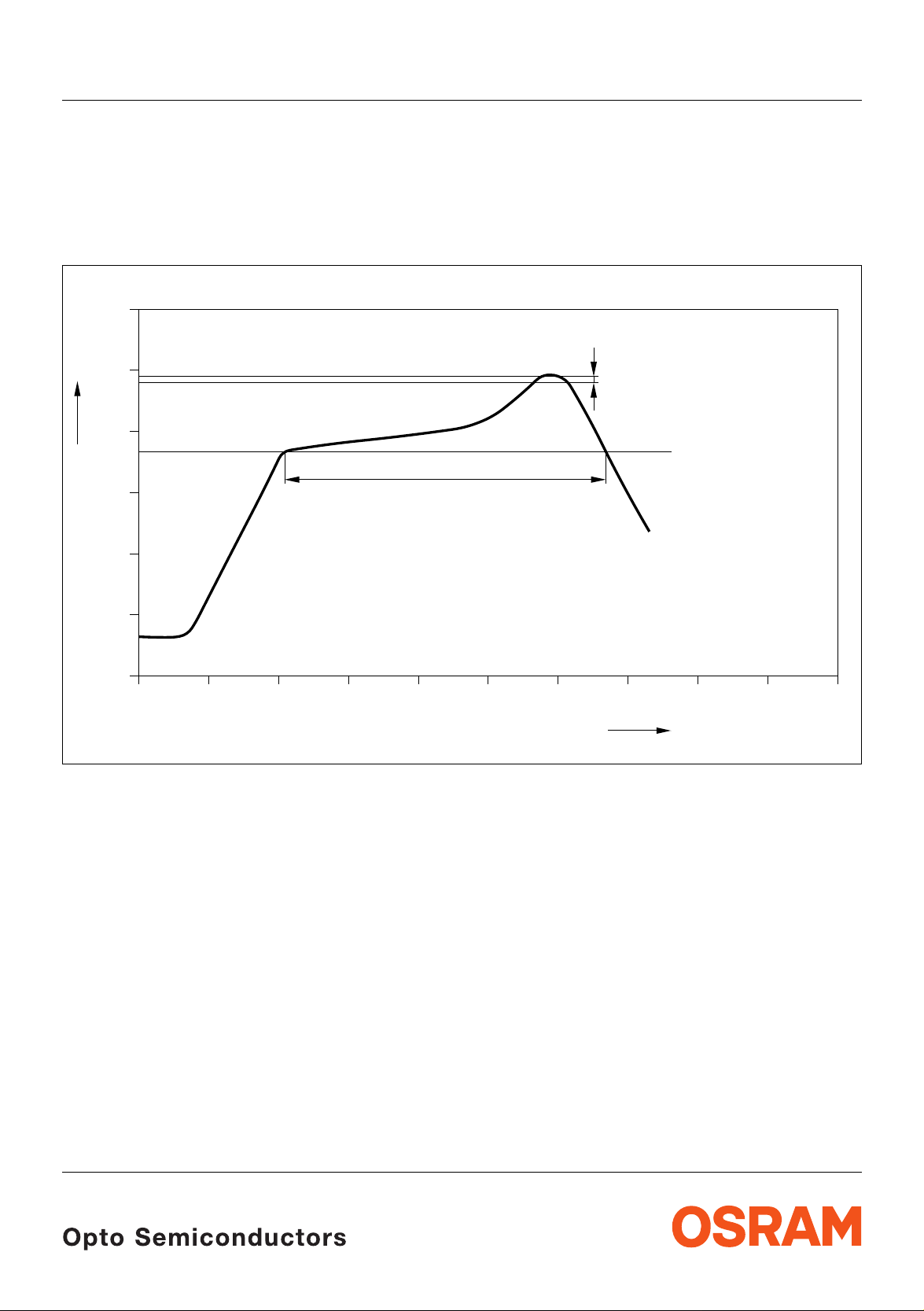
Lötbedingungen Vorbehandlung nach JEDEC Level 2
Soldering Conditions Preconditioning acc. to JEDEC Level 2
IR-Reflow Lötprofil (nach IPC 9501)
IR Reflow Soldering Profile (acc. to IPC 9501)
LATB T66B
300
˚C
250
T
200
120 to 180 s
150
100
Ramp-up rate up to 6 K/s
50
0
0
Defined for Preconditioning: 2-3 K/s
50 100 150 200 250
240-245 ˚C
10-40 s
183 ˚C
Ramp-down rate up to 6 K/s
Defined for Preconditioning: up to 6 K/s
OHLY0597
s
t
2002-05-24 14

Wellenlöten (TTW) (nach CECC 00802)
TTW Soldering (acc. to CECC 00802)
LATB T66B
300
2 K/s
10 s
5 K/s
Zwangskühlung
forced cooling
2. Welle
2. wave
Normalkurve
standard curve
Grenzkurven
limit curves
2 K/s
t
C
250
T
200
150
100
235 C
CC... 130100
50
0
0
C... 260
1. Welle
1. wave
ca 200 K/s
50 100 150 200 250
OHLY0598
s
2002-05-24 15

Empfohlenes Lötpaddesign IR Reflow Löten
Recommended Solder Pad IR Reflow Soldering
LATB T66B
2.6 (0.102)
1.1 (0.043)
1.5 (0.059)
4.5 (0.177)
Padgeometrie für
verbesserte Wärmeableitung
Paddesign for
improved heat dissipation
3.3 (0.130)
3.3 (0.130)
0.4 (0.016)
0.5 (0.020)
7.5 (0.295)
2
_
Kathoden Markierung / Cu Fläche / 12 mm per pad
Cathode marking
Cu-area
<
Lötstoplack
Solder resist
OHLPY439
Maße werden wie folgt angegeb en: m m (inch) / Dimensions are specified as follows: mm (inch).
2002-05-24 16

Empfohlenes Lötpaddesign Wellenlöten (TTW)
Recommended Solder Pad TTW Soldering
6.1 (0.240)
2.8 (0.110)
2 (0.079)
8 (0.315)
6 (0.236)
2 (0.079)
3 (0.118)
3.5 (0.138)
3.5 (0.138)1 (0.039)
1.5 (0.059)
2 (0.079)
LATB T66B
PCB-direction
Bewegungsrichtung
der Platine
2.8 (0.110)
Padgeometrie für
0.5 (0.020)
7.5 (0.295)
verbesserte Wärmeableitung
Paddesign for
improved heat dissipation
Cu Fläche / > 12 mm per pad
Cu-area
2
Lötstoplack
Solder resist
Maße werden wie folgt angegeb en: m m (inch) / Dimensions are specified as follows: mm (inch).
Gurtung / Polarität und Lage Verpackungseinheit 2000/Rolle, ø180 mm
oder 8000/Rolle, ø330 mm
Method of Taping / Polarity and Orientation Packing unit 2000/reel, ø180 mm
or 8000/reel, ø330 mm
1.5 (0.059) 4 (0.157)
2 (0.079)
CC
OHAY0583
8 (0.315)
1.75 (0.069)
2.9 (0.114)
4 (0.157)
3.5 (0.138)
3.6 (0.142)
Maße werden wie folgt angegeb en: m m (inch) / Dimensions are specified as follows: mm (inch).
2002-05-24 17
CA
OHAY0095

Revision History: 2002-05-24
Previous Version: 2001-11-30
Page Subjects (major changes since last revision)
1 ESD-withstand voltage
2 ordering informaion
5 grouping information
LATB T66B
Published by OSRAM Opto Semiconductors GmbH & Co. OHG
Wernerwerkstrasse 2, D-93049 Regensburg
© All Rights Reserved.
Attention please!
The information describes the type of component and sha ll not be considered as assured characteristics.
Terms of delivery and rights to change design reserved. Due to technical requirements components may contain
dangerous substances. For information on the types in question please contact our Sales Organization.
If printed or downloaded, please find the latest version in the Inte rnet .
Packing
Please use the recycling operators k nown to you . We can als o help you – get in touch wit h your near est sales offic e.
By agreement we will take p acking material back, if it is sorted. You m ust bear the costs of transport. For packing
material that is returned to us unsorted or which we are not obliged to accept, we shall have to invoice you for any costs
incurred.
Components used in life-support devices or systems must be expressly authorized for such purpose! Critical
components
1
A critical component is a co mponent used in a life -support device or syst em whose failure ca n reasonably be expecte d
to cause the failure of that life-support device or system, or to affect its safety or the effectiveness of that device or
system.
2
Life support devices or systems are intend ed (a) to be impl anted i n t he human b ody , or (b ) to supp ort a nd/or ma inta in
and sustain human life. If th ey fail , it is rea so nable to assume that the health of the us er m ay be endangered.
2002-05-24 18
1
may only be used in life-support dev ic es or sys t em s 2 with the express written approval of OSRAM OS.

This datasheet has been download from:
www.datasheetcatalog.com
Datasheets for electronics components.
 Loading...