

Page 1

Model FTA820A Octal Fast Timing Amplifier
and
Model FTA420C Quad Fast Timing Amplifier
Operating Manual
Printed in U.S.A. ORTEC® Part No. 740350 1002
Manual Revision D
Page 2

ii
y
y
y
y
y
y
y
g
y
q
g
y
g
g
g
)
q
y
g
g
g
y
y
g
g
y
g
y
y
$GYDQFHG 0HDVXUHPHQW 7HFKQRORJ\ ,QF
a/k/a/ ORTEC®, a subsidia ry of AMETEK®, Inc.
WARRANTY
ORTEC * w arr ant s th at th e ite ms w ill be deliver ed fre e from d efect s in mater ial or wo rkman sh ip. OR TEC makes
no other warranties, express or implied, and specificall
FITNESS FOR A PARTICULAR PURPOSE.
NO WARRANTY OF MERCHANTABILITY OR
ORTEC’s exclusive liabilit
be defectiv e in workmanship or material s within one
claim of any kind, including negligence, loss, or damages arising out of, connected with, or from the
perform ance or breach t hereof , or f rom t he m anuf act ure, sale, del i ver
services covered b
or service furnished or an
or deliver items called for in this a
remed
be liabl e for special or conse
shall be release of the buyer from the obligation to pay the purchase pri c e. In no event shall ORTEC
this agreement or purchase order, shall in no case exceed the price allocabl e to the item
is lim i ted t o repairi ng or replaci ng at ORTEC’s option, i tems found by ORTEC to
ear from t he date of del i very. ORTEC’s liability on an
, resale, repai r, or use of a ny item or
part thereof that gives rise to the claim. In the event O RTEC fai ls to manufacture
reeme nt or pu rchas e ord er, ORTE C’s e xclusive liab ility and buyer’s exclusive
uential damages.
Quality Control
Before being approved for shipment, each ORTEC instrument must pass a stringent set of quality control tests
ned to expose any flaws in materials or workmanship. Permanent records of these tests are maint ained
desi
for use in warrant
repair and as a source of statistical inf or mation for design improvements.
Repair Service
If it becomes necessary to return this instrument for repair, it is essential that Customer Services be contacted
in advance of its return so that a Return Authorization Number can be assi
be informed, either in writin
the nature of the fault of th e instru ment bei n
numbers. Fai lure to do so may cause unnecessa ry delays in getting the unit repai red. The ORT EC
panel
standard procedure re
for new-producti on instrum ents. Instrument s t hat are retur ned should be packed so that the
normal t ransit handl in
nated ORTEC repair center. The address label and the package should include the Return Authorization
desi
Numb e r assi
repaired at t he sender's expense, and it will be the sender's responsibilit
Instrument s not in warrant
ned. Instrum ents being returned that ar e dam aged in transit due to i nadequate packing will be
, by telephone [(865) 482-4411] or by facsimile transmission [(865) 483-2133], of
returned and of the m odel , seri al , and revi sion (“Rev” on rear
uires that instruments returned for repair pass the same quality control tests that are used
and must be shipped PREPAID vi a Ai r P ar cel Post or United Parcel Serv ice to t he
should fol low the same procedure and ORTEC will provide a quotation.
ned to the unit. Also, ORTEC must
will withstand
to make cl aim wit h the shipper.
Shipments should be examined immediately upon receipt for evidence of external or concealed damage. The
carrier makin
for dam a
order to establish clai ms. After such notif ication to the carrier, please not if
that assistance can be provided in makin
necessar
Copyright © 2002, Advanced Measurement Technology, Inc. All rights reserved.
*ORTEC
the propert
delivery should be notified immediately of any such damage, since the carrier is normally liable
e in shipment. Packing materials, waybills, and other such docum ent ati on shoul d be preserved in
.
®
is a registered trademark of Advanced Measurement Technology, Inc. All ot her tr adem ar ks used herein are
of their respective owners.
Damage in Transit
ORTEC of t he c ircumstances so
damage claims and in providing replacement equipment, if
Page 3

iii
CONTENTS
SAFETY INSTRUCTIONS AND SYMBOLS ............................................... iv
SAFETY WARNINGS AND CLEANING INSTRUCTIONS ..................................... v
1. DESCRIPTION ................................................................... 1
2. SPECIFICATIONS ................................................................ 1
2.1. PERFORMANCE............................................................. 1
2.2. ELECTRICAL AND MECHANICAL................................................ 1
3. INSTALLATION .................................................................. 1
4. CIRCUIT DESCRIPTION ........................................................... 2
5. MAINTENANCE .................................................................. 2
Page 4

iv
SAFETY INSTRUCTIONS AND SYMBOLS
This manual contains up to t hr ee levels of safet y instructi ons that must be observed in order to avoid
personal injur y and/or damage to equipment or other property. These are:
DANGER
WARNING
CAUTION
Please read all safety instr uc tions carefully and m ak e sure you under stand them fully before attempting t o
use this product.
In addition, the following sym bol may appear on t he pr oduc t:
Indicates a hazard that could resul t in death or serious bodi ly harm if the safety instruc tion is
not observed.
Indicates a hazard that could resul t in bodil y har m if the safety instruction is not observed.
Indicates a hazard that could resul t in property damage if the safety instruction is not
observed.
ATTENTION – Refer to Manual
DANGER – High Voltage
Please read all safety instr uc tions carefully and m ak e sure you under stand them fully before attempting t o
use this product.
Page 5

v
SAFETY WARNINGS AND CLEANING INSTRUCTIONS
DANGER Opening the cover of this instr ument is likely t o expose dangerous vol tages. Disconnect the
instrument from all volt age sources whil e it is being opened.
WARNING Using this i nstr ument in a manner not specified by the manufacturer may impair the
protecti on pr ovi ded by the instrument.
Cleaning Instructions
To clean the instrument exterior :
Unplug the instr ument from the ac power supply.
Remove loose dust on the outside of the instr ument with a l int-free cloth.
Remove remaining dirt with a lint- free cl oth dampened in a general-purpose detergent and water
solution. Do not use abrasive c leaners.
CAUTION To prevent moisture i nsi de of the instr ument during external c leaning, use only enough liquid
to dampen the c loth or applicator.
Allow the i nstr ument to dry c ompletely before rec onnec ting it to the power source.
Page 6
vi
Page 7

1
ORTEC MODEL FTA820A OCTAL FAST TIMING AMPLIFIER
AND MODEL FTA420C QUAD FAST TIMING AMPLIFIER
1. DESCRIPTION
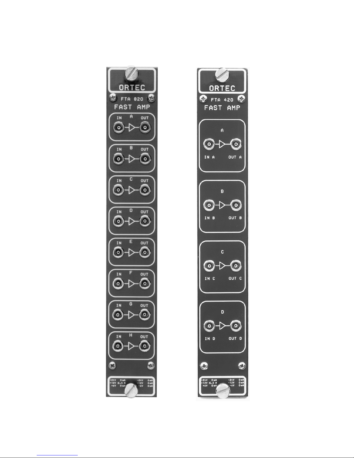
The Model FTA820A and FTA420C Fast Timing
Amplifiers are high-performance, wide-bandwidth
amplifiers designed for boosting very fast linear
signals from photomultipliers, elec tron multipliers,
silicon surface-barrier detectors, and other
detectors used in fast timing applications. The rise
time on both versions is <1 ns with a 5-V output,
enabling excellent timing resolution.
2. SPECIFICATIONS
2.1. PERFORMANCE
GAIN FOR EACH CHANNEL
on both versions):
FTA820A
FTA420C
NUMBER OF CHANNELS
FTA820A
FTA420C
RISE TIME
200, noninverting.
20, noninverting.
8
4
1 ns.
(10% gain tolerance
Both units are single-width NIM modules. The
FTA820A is an 8-channel unit with a gain of 200,
noninverting. The 4-channel FTA420C offers a gain
of 20, noninverting. LEMO type 00C50 connectors
are used for all signal c onnec tions.
INPUTS One per channel. LEMO connector; input
impedance 50 .
OUTPUTS One per channel. LEMO connector;
0 to 5V output with a 50- load. Output
impedance
1 .
2.2. ELECTRICAL AND MECHANICAL
POWER REQUIRED
FTA820A +12 V, 400 mA.
FTA420C +12 V, 200 mA.
NOISE
BANDWIDTH 10 to 350 MHz.
PROPAGATION DELAY
channels.
OUTPUT RANGE 0 to 5 V with 50- load.
20 µV rms equivalent input noise.
30-ps variation between
3. INSTALLATION
The FTA820A and FTA420C contain no internal
power supply and must obtain power from a NIMstandard bin and power supply. The bin and power
supply should be turned Off when modules are
inserted and removed. The power supply voltages
should be checked after modules are inserted.
DIMENSIONS Standard single-width NIM module,
3.4 cm × 22.1 cm (1.35 in. × 8.714 in.) per
DOE/ER-0457T.
WEIGHT
Net 1 kg (2.2 lb).
Shipping 2.7 kg (5.9 lb).
Ensure that the unit has sufficient cooling air
circulating to prevent any localized heating of the
solid-state circuitry used throughout the module.
The FTA820A and FTA420C should not be
subjected to temperatures in excess of 50(C.
Page 8

2
4. CIRCUIT DESCRIPTION
The FTA820A Amplifier has a noninverting gain of
200. Th e FT A420C has a noninverti ng gai n of 20.
The FTA820A is composed of eight separate
amplifiers; the FTA420C has four separate
amplifiers. The amplifiers are constructed on a
single printed wiring board. Each section is
identical, and the circuit description that follows
relates to any of the four sections. Component
designations are the same for each channel except
that channel 1 components have a prefix of “1”,
channel 2 components have a prefix of “2”, and so
on for al l four c hannels.
The “A” v ersion has five gain stages, 1Q1 through
1Q4, connected in the Common-Emitter
confi guration, and 1Q 5 connected in the Em itterFollower configuration. Each stage is ac-coupled to
isolate bias voltages and to strongly reject lowfrequency components. In put protection is furnished
by diode 1D1.
Consider the first stage formed around 1Q1.
Resistor 1R2 furni shes base-injection bi as for the
transistor, the series combination 1C2 and 1R3
provi des shunt feedback, and resistor 1R4 is an
unbypassed emitter resistor which, along with 1C3,
peaks the high-frequency response of the stage.
Each of the other Common-Emitter stages operated
in a similar manner with specific component values
set for optimum gain distribution and rise time. The
final t wo Com mon-Em itter stages, 1Q 3 and 1Q4,
have variable peaking capacitors, 1C20 and 1C21,
which are set in test to gi ve an over all r ise time of
<1 ns. Transistor 1Q5 is connected i n the Em i t terFollower configuration and provides excellent
output driv e capability, 0 to 5 V, and l ow output
impendence, <1 .
The grounding f or each secti on of t he am pli fi er is
isolated f rom the f rame ex cept at th e f ront panel .
Each individual amplifier section receives its circuit
ground v ia coax to the front panel, and a highquality ground connecti on must be m aint ained f or
proper operation.
The “ C” version has two fewer Common-Emitter
ampli fi er stages than the “A” v e rsi on . There i s no
signal inversion from input to output, and the
overall gain is nominally 20. The operation of each
stage is similar to that of the “A” version except for
the di stri bution of gain and rise time among the
vari ous ampl ifier stages. P eaking capacitors 1C3
and 1C7 are set in test to give an overall rise t ime
<1 ns.
5. MAINTENANCE
The FTA820A and FTA420C require very little maintenance other than routine removal of dust and tightening
of mechanical connections.
of this manual.
Be sure to observe the cleaning instructions and s afety warnings a t the fr ont
Page 9
3
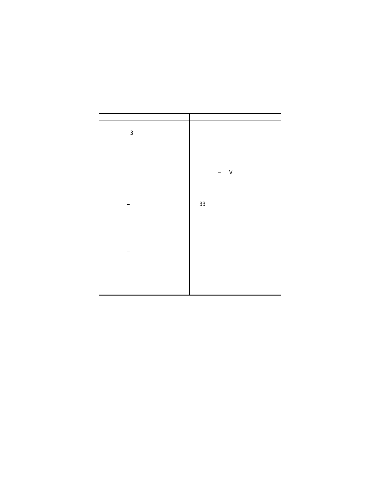
Bin/Module Connector Pin Assignments for Standard
Nuclear Inst rument Modules per DOE/ER-0457T
Pin Function Pin Function
1 +3 V 23 Reserved
2
3 V
3 Spare Bus 25 Reserved
4 Reserved Bus 26 Spare
5 Coaxial 27 Spare
6 Coaxial *28 +24 V
7 Coaxial *29
8 200 V dc 30 Spare Bus
9 Spare 31 Spare
*10 +6 V 32 Spare
*11
12 Reserved Bus *34 Power Return Ground
13 Spare 35 Reset (Scaler)
14 Spare 36 Gate
15 Reserved 37 Reset (Auxiliary)
*16 +12 V 38 Coaxial
*17
18 Spare Bus 40 Coaxial
19 Reserved Bus *41 117 V ac (Neutral)
20 Spare *42 High-Quali ty Ground
21 Spare G Ground Gui de Pin
22 Reserved
6 V
12 V
24 Reserved
24 V
*33 117 V ac (Hot)
39 Coaxial
Pins marked (*) ar e inst al led and wired in ORTEC’s Model 4001A and
4001C Modular System Bins.
Page 10

4
 Loading...