

Page 1

H
ARDWARE REFERENCE GUIDE
Date : 28 November 2005
Doc. no. : C6713CPU_HRG
Iss./Rev : 1.1
Page : 1
Orsys Orth System GmbH, Am Stadtgraben 25, 88677 Markdorf
,
Germany http://www.orsys.de
Hardware Reference Guide
micro-line
C6713CPU
High performance DSP / FPGA board
Page 2

H
ARDWARE REFERENCE GUIDE
MICRO-LINE
C6713CPU
Date : 28 November 2005
Doc. no. : C6713CPU_HRG
Iss./Rev : 1.1
Page : 2
Contents
1 PREFACE......................................................................................................................6
1.1 Document Organization.........................................................................................................6
1.2 Documentation Overview ......................................................................................................6
1.3 Notational conventions..........................................................................................................6
1.4 Trademarks.............................................................................................................................7
1.5 Revision History.....................................................................................................................8
2 HARDWARE OVERVIEW .............................................................................................9
2.1 Block Diagram of the C6713CPU ........................................................................................10
2.2 Connectors ...........................................................................................................................12
2.2.1 micro-line® Connectors........................................................................................................ 12
2.2.2 JTAG Connector.................................................................................................................. 12
2.3 Interfaces and Hardware Components...............................................................................12
2.3.1 FPGA................................................................................................................................... 12
2.3.2 External Memory (on-board SDRAM).................................................................................. 13
2.3.3 Flash Memory...................................................................................................................... 14
2.3.4 PLD .....................................................................................................................................14
2.3.5 UART / RS-232 Interface .................................................................................................... 14
2.3.6 Temperature Sensor ........................................................................................................... 14
2.3.7 Reset Generator and Watchdog.......................................................................................... 15
2.3.8 External Flags (XF signals) ................................................................................................. 15
2.3.9 Power Supply of the Board.................................................................................................. 15
2.4 Status LED's .........................................................................................................................15
2.4.1 User Programmable LED's (PLD) .......................................................................................16
2.4.2 User Programmable LED (FPGA) .......................................................................................16
2.5 DSP peripherals....................................................................................................................16
2.5.1 Multichannel Audio Serial Ports (McASP) ...........................................................................16
2.5.2 External Memory Interface (EMIF) ......................................................................................16
2.5.3 Inter Integrated Circuit (I2C) Interfaces................................................................................ 17
2.5.4 General Purpose Input / Output Pins (GPIO) ...................................................................... 17
2.5.5 Multi-channel Buffered Serial Ports (McBSP)...................................................................... 17
2.5.6 Timers .................................................................................................................................18
2.5.7 Host Port Interface (HPI) ..................................................................................................... 18
2.5.8 Interrupts ............................................................................................................................. 18
2.5.9 DMA ....................................................................................................................................19
3 MEMORY MAPS AND DESCRIPTION OF THE PLD REGISTERS ...........................20
3.1 TMS320C6713 Memory Map ................................................................................................20
3.2 C6713CPU Address Map......................................................................................................21
Page 3

H
ARDWARE REFERENCE GUIDE
MICRO-LINE
C6713CPU
Date : 28 November 2005
Doc. no. : C6713CPU_HRG
Iss./Rev : 1.1
Page : 3
3.3 Internal fast SRAM ...............................................................................................................21
3.4 DSP Peripherals ...................................................................................................................21
3.5 External SDRAM...................................................................................................................21
3.6 Flash Memory .......................................................................................................................21
3.7 Endianness ...........................................................................................................................22
3.8 EMIF Configuration ..............................................................................................................23
3.8.1 Default EMIF configuration.................................................................................................. 23
3.9 Description of the PLD Board Registers............................................................................23
3.10 Description of the PLD Registers .....................................................................................24
3.10.1 Hardware Configuration Register (HWCFG) .....................................................................24
3.10.2 FPGA Control Register (FCR)........................................................................................... 25
3.10.3 LED Control Register (LED) ..............................................................................................25
3.10.4 Module Control Register (MCR) ........................................................................................ 26
3.10.5 I2C Bus Control Register (I2C) ..........................................................................................26
3.10.6 External Flag Register (XF)............................................................................................... 27
3.10.7 Watchdog Register (WDG)................................................................................................ 27
3.10.8 Version Register (VER) ..................................................................................................... 28
4 BOOT PROCESS AND DEFAULT SETUP OF THE C6713CPU................................29
5 USING THE FLASH FILE SYSTEM............................................................................30
6 DESCRIPTION OF THE MICRO-LINE® BOARD CONNECTORS..............................31
6.1 Location of the Connectors.................................................................................................31
6.2 Connector Overview ............................................................................................................32
6.3 Pinout Tables of the micro-line® Connector ......................................................................32
6.4 Pinout of the JTAG Connector............................................................................................35
6.5 Function of the micro-line® Connector Pins......................................................................36
6.5.1 Connector A ........................................................................................................................ 36
6.5.2 Connector B ........................................................................................................................ 36
6.5.3 Connector BB ...................................................................................................................... 36
6.5.4 Connector D ........................................................................................................................ 37
6.5.5 Connector E ........................................................................................................................ 38
7 ENVIRONMENT ..........................................................................................................44
7.1 Minimum Connections.........................................................................................................44
7.2 Changing the Board Configuration.....................................................................................46
7.2.1 Location of modifiable components..................................................................................... 46
7.2.2 Configuring DSP Clock Speed ............................................................................................ 47
Page 4

H
ARDWARE REFERENCE GUIDE
MICRO-LINE
C6713CPU
Date : 28 November 2005
Doc. no. : C6713CPU_HRG
Iss./Rev : 1.1
Page : 4
7.2.3 Configuring for HPI or McASP1 Usage ...............................................................................47
7.2.4 Configuring micro-line® Pin D30 Termination ...................................................................... 47
7.2.5 Configuring for I2C interface #0 Operation ..........................................................................47
7.2.6 Configuring CLKS1 / SCL1 Termination.............................................................................. 48
7.2.7 Configuring FPGA I/O Behavior When FPGA is not Loaded............................................... 48
7.3 Signal Levels and Loads .....................................................................................................48
7.3.1 Input Voltage Levels for non-FPGA Signals........................................................................ 48
7.3.2 Output Voltage Levels for non-FPGA Signals .....................................................................48
7.3.3 Allowed Output Loads ......................................................................................................... 48
7.4 Supply Voltage .....................................................................................................................49
7.5 Power Consumption ............................................................................................................49
7.6 Reset Timing.........................................................................................................................49
7.7 Ambient Temperature ..........................................................................................................49
7.8 Ambient Humidity.................................................................................................................49
7.9 Dimensions of the Board.....................................................................................................50
7.10 Spare micro-line® Connectors...........................................................................................52
8 LIST OF ABBREVIATIONS USED IN THIS DOCUMENT ..........................................53
9 LITERATURE REFERENCES.....................................................................................54
Page 5

H
ARDWARE REFERENCE GUIDE
MICRO-LINE
C6713CPU
Date : 28 November 2005
Doc. no. : C6713CPU_HRG
Iss./Rev : 1.1
Page : 5
List of Tables
Table 1: Memory map of the processor........................................................................................... 20
Table 2: Memory map of the C6713CPU ........................................................................................ 21
Table 3: default initialization values for the FPGA related CE space registers ...............................23
Table 4: CE2 default configuration .................................................................................................. 23
Table 5: CE3 default configuration .................................................................................................. 23
Table 6: PLD and UART registers of the C6713CPU...................................................................... 24
Table 7: PLD register quick reference.............................................................................................24
Table 8: Version register encoding.................................................................................................. 28
Table 9: Default clock and EMIF settings of the C6713CPU........................................................... 29
Table 10: Connector overview......................................................................................................... 32
Table 11: Pinout of the micro-line® connectors ...............................................................................32
Table 12: Pinout summary for the McBSP interfaces...................................................................... 33
Table 13: Pinout summary for the timers ........................................................................................33
Table 14: Pinout summary for the I2C interfaces............................................................................. 33
Table 15: Pinout summary and signal routing for the McASP interfaces ........................................ 34
Table 16: Pinout of the JTAG connector .........................................................................................35
Table 17: Factory default configuration summary ...........................................................................46
Table 18: Voltage limits for the C6713CPU..................................................................................... 49
Table 19: Power consumption of the C6713CPU............................................................................ 49
Table 20: Reset timing ....................................................................................................................49
List of Figures
Figure 1: Block diagram of the C6713CPU ..................................................................................... 10
Figure 2: Top side of the C6713CPU ..............................................................................................11
Figure 3: Bottom side of the C6713CPU ......................................................................................... 11
Figure 4: FPGA connections overview ............................................................................................ 13
Figure 5: Data representation in memory in little endian configuration ...........................................22
Figure 6: Connector locations .........................................................................................................31
Figure 7: JTAG adapter for the C6713CPU ....................................................................................35
Figure 8: Supplying the C6713CPU with power .............................................................................. 44
Figure 9: Connecting the serial interface (RS-232) to a PC ............................................................ 45
Figure 10: Location of configuration elements (top side) ................................................................46
Figure 11: Location of configuration elements (bottom side) ..........................................................47
Figure 12: Dimensions of the C6713CPU (in millimeters)............................................................... 50
Figure 13: Complete micro-line® footprint........................................................................................ 51
Figure 14: C6713CPU connector pins............................................................................................. 52
Page 6

H
ARDWARE REFERENCE GUIDE
MICRO-LINE
C6713CPU
Date : 28 November 2005
Doc. no. : C6713CPU_HRG
Iss./Rev : 1.1
Page : 6
1 Preface
This document describes the hardware of the C6713CPU board. It is intended to get an overview
of the board and its features. Detailed information about programming, usage of the FPGA and the
DSP is described in other documents that will be referenced throughout this document.
1.1 Document Organization
This document is organized as follows:
Chapter 2 gives an overview of the whole system and its interfaces
Chapter 3 gives an overview of the memory maps and describes the PLD registers
Chapter 4 describes the boot process and the default settings of the board
Chapter 5 gives a brief introduction to the Flash File System of the board
Chapter 6 describes externally available signals and connector pinouts
Chapter 7 lists environmental conditions, such as voltage levels, temperature range, etc.
Chapter 9 lists documents that contain further information
Chapter 8 explains the abbreviations that are used throughout this document
1.2 Documentation Overview
This chapter lists the documentation from ORSYS that is shipped together with the C6713CPU.
Further documents from other vendors may also be listed in chapter 9 and are referenced
throughout this document in square brackets.
C6713CPU DSP Development Kit User's Guide [20]
(
C6713CPU_DSP_DevKit_ug.pdf
):
This document describes software development for the C6713CPU board using DSP/BIOS and the
C6713CPU
board library. The board library is a collection of low level drivers that allow to access
hardware on the C6713CPU, such as loading the FPGA, reading the temperature sensor etc. This
makes working with the C6713CPU easier.
C6713CPU micro-line
®
busmaster BSP User's Guide [21] (
C6713CPU_ml_bm_ug.pdf
):
Describes the micro-line
®
busmaster board support package (BSP). This BSP adds an
asynchronous parallel bus peripheral interface, an UART and HPI accessibility to the C6713CPU.
The user guide includes FPGA register description and FPGA register programming
documentation.
C6713CPU FPGA Programming Guide [22] (
C6713CPU_FPGA_pg.pdf
)
Describes how to develop customized FPGA designs. Part of the FPGA development kit.
Micro-line
®
Power Supply Kit [23] (
Power_Supply.pdf
):
Describes the micro-line
®
Power Supply board.
Reference documents that contain further information are listed in chapter 9, "Literature
References”. References to these documents are given in square brackets throughout this
document.
1.3 Notational conventions
Names of registers, bit fields and single bits are written in capital letters.
Example:
HWCFG
Names of signals are also given in capital letters, active low signals are marked with a '/' at the
beginning of the name.
Example:
/RESETIN
Page 7
H
ARDWARE REFERENCE GUIDE
MICRO-LINE
C6713CPU
Date : 28 November 2005
Doc. no. : C6713CPU_HRG
Iss./Rev : 1.1
Page : 7
Configuration parameters, function names, path names and file names are written in italic typeface.
Example:
dev_id
Source code examples are given in a small, fixed-width typeface.
Example:
int a = 10;
Menus and commands from menus and submenus are enclosed in double-quotes. Example:
Create a new project using the "Create Project..." command from the "File" menu.
The members of a bit field or a group of signals are numbered starting at zero, which is the least
significant bit.
Example:
CFG[4:0] identifies a group of five signals, where CFG0 is the least significant bit and
CFG4 is the most significant bit.
If necessary, numbers are represented with a suffix that specifies their base.
Example: 12AB
16
is a hexadecimal number (base 16 = hexadecimal) and is equal to 477910.
The bit fields of a register are displayed with the most significant bit to the left. Below each bit field
is a description of its read / write accessibility and its default value:
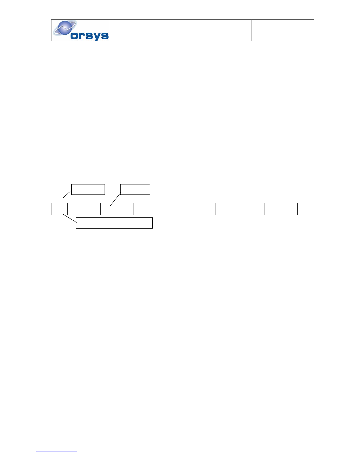
15 14 13 12 11 10 9 8 7 6 5 4 3 2 1 0
A B C D E F G H I J K L N O
r,w,0 r,w,0 r,w,0 r,w,0 r,w,0 r,w,0 r,w,010
2
r,0 r,wc,0 w r,w,0 rc,0 r,w,0 r,w,0
bit number bit name
accessibility and default value
legend:
r bit is readable
rc this bit is cleared after a read
r,w bit is readable and writeable, reading yields the previously written value unless otherwise
specified.
w bit is writeable, read value is undefined
wc writing a 1 to this bit clears it
w,0 bit is write-only, reading always yields 0.
0 default value
1.4 Trademarks
TI, Code Composer, DSP/BIOS and TMS320C6000 are registered trademarks of Texas
Instruments.
Microsoft
and Windows are either registered trademarks or trademarks of Microsoft Corporation
in the United States and/or other countries.
Hypterterminal is a trademark of Hilgraeve Inc.
All other brand or product names are trademarks or registered trademarks of their respective
companies or organizations.
Page 8
H
ARDWARE REFERENCE GUIDE
MICRO-LINE
C6713CPU
Date : 28 November 2005
Doc. no. : C6713CPU_HRG
Iss./Rev : 1.1
Page : 8
1.5 Revision History
Revision Changes
0.1 ORSYS internal preliminary version / April 2005
0.5 First public preliminary version / May 2005
0.9 Completely revised.
Block diagram completed.
1.0 Flash File System: short description only, reference to separate user's guide.
Mentioned that HPI usage requires FPGA.
Minor corrections to signal descriptions: series resistors, /RESETOUT pull-up, default
state of RTS, recommended usage of D19..D21, SCL0/SDA0 usage, HPI driver
direction control.
Values for typical power consumption added.
Dimensions of connector pins revised.
1.1 Added note about RS-232 usage with Win 2k and XP.
Board dimensions: board and connector height added.
Page 9

H
ARDWARE REFERENCE GUIDE
MICRO-LINE
C6713CPU
Date : 28 November 2005
Doc. no. : C6713CPU_HRG
Iss./Rev : 1.1
Page : 9
2 Hardware Overview
The micro-line® C6713CPU is a high performance DSP board that combines several key
technologies for high speed data processing:
a TMS320C6713 DSP with 256 KB internal fast SRAM and 225MHz or 300MHz CPU clock
(1800 MIPS / 1350 MFLOPS or 2400 MIPS / 1800 MFLOPS)
a Xilinx Spartan 3 FPGA with up to 1M gates
32 / 64 MB SDRAM in standard versions and 128 MB on request
2 MB flash memory for non-volatile program, data and FPGA design storage
The C6713CPU is available in different versions, regarding processor speed and memory size.
Please contact ORSYS or ORSYS distributors for the newest product list.
For proper operation of the micro-line
®
C6713CPU ORSYS recommends the desk carrier micro-
line
®
PowerSupply board which provides:
3.3 V regulated power supply for the C6713CPU
a 9-Pin SUB-D connector for the RS-232 interface
a reset button
Two isolated ±15 V DC/DC converters for peripheral I/O power supply (optional)
ORSYS furthermore offers complete development packages including Code Composer Studio,
XDS510 JTAG emulator/debugger or equivalent types and all necessary accessories like cables,
power supplies and software libraries.
This documentation describes the basic features of the C6713CPU. It does not include details of
the FPGA or the DSP. For further information about the FPGA, please refer to Xilinx [2]. For further
information about the DSP, please refer to Texas Instruments [1]. A good starting point is also the
chapter "documentation support" in [4].
Many operational features of the C6713CPU require the use of a specific FPGA design, which is
provided by an according board support package (BSP).
The FPGA of the C6713CPU can be used either with the default BSP from ORSYS which is preinstalled when the C6713CPU is shipped, or with individual custom designs using the FPGA
development option. The default BSP from ORSYS allows to operate the C6713CPU as a standard
micro-line
®
DSP board. In this case it is logically upward compatible to other existing micro-line
®
products such as the C6711CPU (if the C6711CPU is operated with 3.3V only).
Page 10
H
ARDWARE REFERENCE GUIDE
MICRO-LINE
C6713CPU
Date : 28 November 2005
Doc. no. : C6713CPU_HRG
Iss./Rev : 1.1
Page : 10
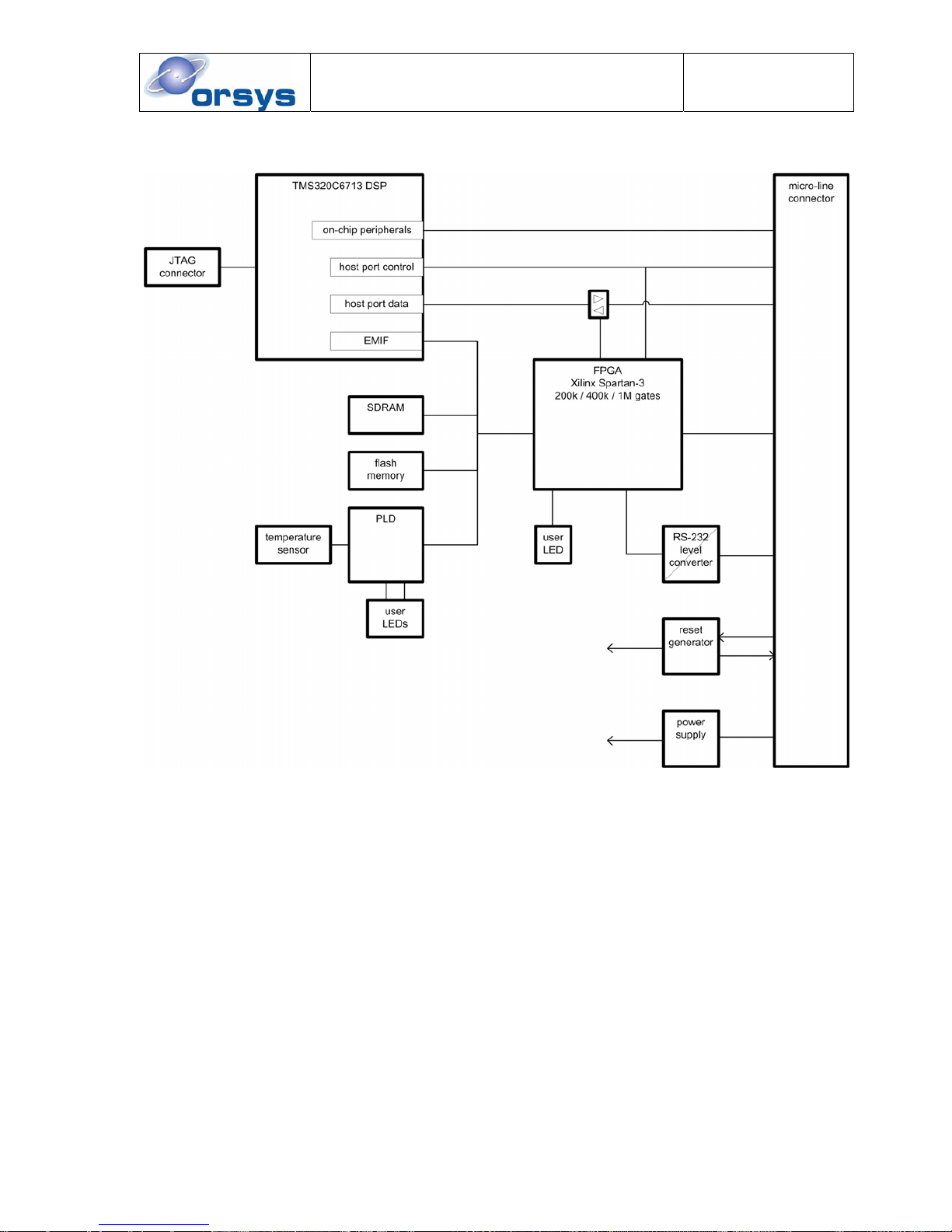
2.1 Block Diagram of the C6713CPU
Figure 1: Block diagram of the C6713CPU
Page 11
H
ARDWARE REFERENCE GUIDE
MICRO-LINE
C6713CPU
Date : 28 November 2005
Doc. no. : C6713CPU_HRG
Iss./Rev : 1.1
Page : 11
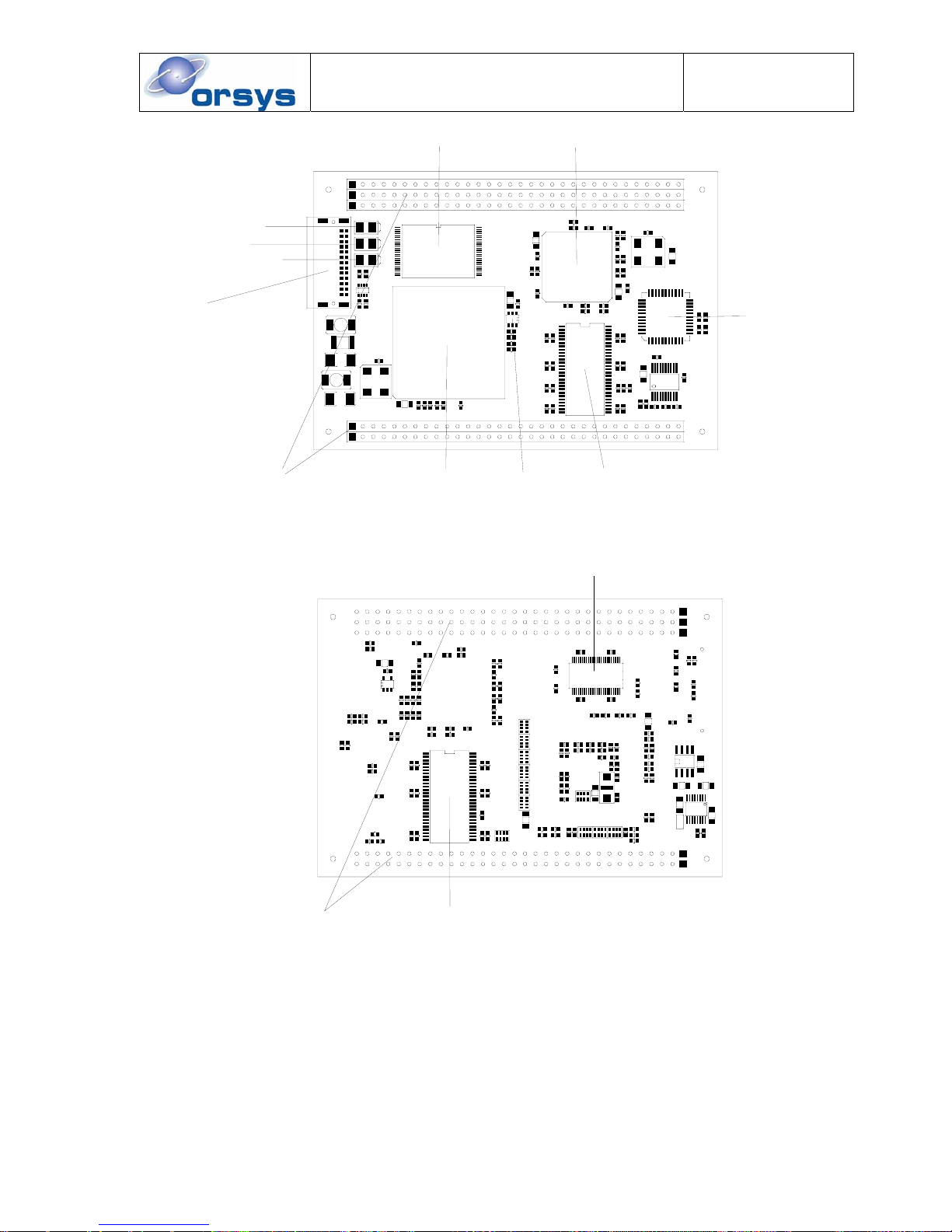
C9
green LED (PLD)
red LED (PLD)
yellow LED (FPGA)
JTAG
connector
DSP SDRAM
temperature
senso
r
flash memory FPG
A
PLD
micro-line connectors
Figure 2: Top side of the C6713CPU
micro-line connectors
R1
SDRAM
16 bit HPI data bus transceiver
Figure 3: Bottom side of the C6713CPU
Page 12

H
ARDWARE REFERENCE GUIDE
MICRO-LINE
C6713CPU
Date : 28 November 2005
Doc. no. : C6713CPU_HRG
Iss./Rev : 1.1
Page : 12
2.2 Connectors
2.2.1 micro-line® Connectors
The micro-line
®
connectors are the main I/O connectors of the C6713CPU. They provide access to
all signals that are needed for a wide range of I/O connectivity. The signals on the micro-line
®
connectors can be grouped into the following categories:
power supply
DSP- and board specific interfaces, such as timers and serial ports
FPGA specific signals (their function depend on the respective FPGA design)
Historically (without FPGA) the micro-line
®
connectors carried the following signals:
power supply
DSP- and board specific interfaces, such as timers and serial ports
the micro-line
®
peripheral interface which allowed straightforward access to peripherals
Today, with FPGA technology onboard, many of the micro-line
®
I/O signals can be individually
hardware-configured for nearly any application. This is possible by building an individual,
application-specific FPGA design which exactly covers the application's requirements.
Nevertheless, the micro-line
®
standard peripheral interface is still available as a board support
package, the micro-line busmaster BSP
®
. It is the default configuration when the C6713CPU board
is shipped from ORSYS. The pinning of the micro-line
®
connectors (without any particular FPGA
design loaded) is described in chapter 6. The pinning and functionality of the micro-line
®
busmaster
BSP is described in [21].
2.2.2 JTAG Connector
The JTAG connector is used during development of application software or FPGA designs. It
contains two separate JTAG interfaces, one for the DSP and one for the FPGA.
The DSP JTAG interface is used for debugging and application software download during
development, together with Texas Instruments Code Composer Studio and an XDS510 (or similar)
emulator. After the software development is finalized, the user application software can be
downloaded from the development PC to the C6713CPU's flash memory via RS232 for permanent
storage. This is managed by the Flash File System which is permanently installed on the
C6713CPU.
The FPGA JTAG interface can be used to quickly download and test FPGA designs during
development without permanent storage on the C6713CPU. After the FPGA development is
finalized, the FPGA design can be downloaded from the development PC via RS232 to the
C6713CPU's flash memory for permanent storage. This is managed by the Flash File System
which is permanently installed on the C6713CPU.
In order to connect a standard DSP JTAG emulator or a standard FPGA download cable to the
C6713CPU, a JTAG adapter is used, which is included in C6713CPU development kits. The JTAG
adapter is described in chapter 6.4.
2.3 Interfaces and Hardware Components
2.3.1 FPGA
The default FPGA design for the C6713CPU can be used for standard micro-line
®
bus compatible
applications. Alternatively the FPGA can be individually programmed by the user. This is possible
by using an optional FPGA development package from ORSYS together with standard FPGA
development tools from Xilinx. FPGA technology allows flexible internal logic and individual I/O
Page 13
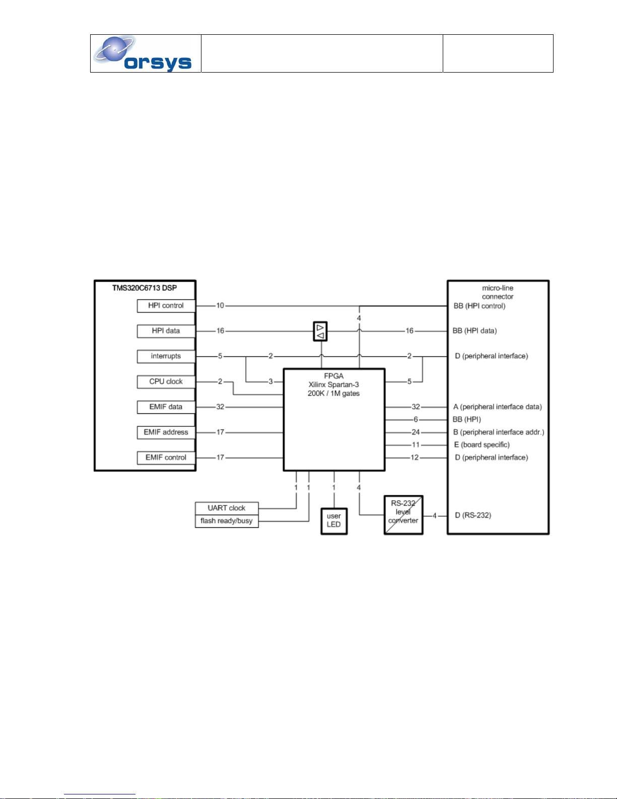
H
ARDWARE REFERENCE GUIDE
MICRO-LINE
C6713CPU
Date : 28 November 2005
Doc. no. : C6713CPU_HRG
Iss./Rev : 1.1
Page : 13
interfacing over for the majority of the micro-line
®
connector pins. The user is no longer restricted
to a fixed I/O logic.
The FPGA has access to the following signal groups:
DSP EMIF (data bus, address bus, control signals)
micro-line
®
connectors
JTAG interface
DSP interrupts
RS232 line driver
The figure below gives an overview, how the FPGA is connected on the C6713CPU board. The
numbers shows the number of signals for each connection. The description of the micro-line
®
connectors in parentheses show the classic functions, as they are implemented by the micro-line
®
busmaster BSP (see [21]) and also by classic micro-line
®
CPU and peripheral boards without
FPGA.
Figure 4: FPGA connections overview
After power up or hardware reset, the FPGA is automatically cleared and has to be loaded before it
starts operation. This can be done manually by application software or automatically by the Flash
File System of the C6713CPU. The FPGA can be loaded at any time and can also be reloaded
with a different configuration during runtime without the need to power-off or reset the whole board.
During system startup, a FPGA design is loaded by the Flash File System (see chapter 2.3.3). This
FPGA design leaves all external pins passive, except the RS-232 interface. For a more detailed
description of the FPGA signals, please refer to the documentation of the micro-line busmaster
BSP [21] or FPGA development [22].
2.3.2 External Memory (on-board SDRAM)
The C6713CPU uses 32-bit wide SDRAM with 32 or 64 MB in standard off-the-shelf versions and
up to 128 MB on request. This provides a large memory space for storage of program code or
data. The memory access timings are based on the EMIF clock which is initialized to 90 MHz
(225 MHz CPU clock) or 100 MHz (300MHZ CPU clock) by the Flash File System. The EMIF clock
Page 14

H
ARDWARE REFERENCE GUIDE
MICRO-LINE
C6713CPU
Date : 28 November 2005
Doc. no. : C6713CPU_HRG
Iss./Rev : 1.1
Page : 14
can be software reconfigured by PLL settings. It can also be generated by the FPGA, allowing any
clock frequency up to 100 MHz.
Compared to the internal fast SRAM of the DSP chip, the on-board SDRAM is significantly slower.
Therefore it is strongly recommended to use the internal memory of the DSP whenever it is
possible. The internal memory can be used as memory for time critical code and data as well as L2
cache. See [4] for details.
2.3.3 Flash Memory
The C6713CPU uses an MX29LV160BT flash memory for non-volatile storage. The flash memory
is 16 bit wide and can hold up to 2 MB. It is used for permanent storage of software- and FPGA
code.
After reset or power up, the DSP boots from the first address of the flash memory. The DSP
internal boot loader copies the first 1 KB to internal memory to address 0 and executes it. Further
loading is realized by a secondary loader program.
The C6713CPU is always shipped with the Flash File System installed. It handles all flash memory
programming and management of stored data. The Flash File System is automatically booted after
reset or power up. It first initializes the system, then looks for commands from a host on the RS232 interface (See [24] for a description of the host side utilities) and then loads the FPGA(s) and a
user program that are selected for auto-boot. Since RS-232 usage on the C6713CPU requires a
loaded FPGA design, the Flash File System already contains a startup FPGA design, which is
loaded during system startup. Later on it will be overwritten when the on-board auto-boot FPGA is
loaded.
2.3.4 PLD
The PLD contains some necessary glue logic of the board. It provides all necessary resources to
run the DSP without a loaded FPGA. It also contains some register that configure board operation.
See chapter 3.10 for a description of the PLD registers,
2.3.5 UART / RS-232 Interface
The RS-232 interface is realized inside the FPGA and is connected to a RS-232 line driver.
Therefore, to use the RS-232 interface, an appropriate FPGA design must be loaded. The RS-232
interface can be used as general purpose communication interface. Functions like
fprintf(), and
fgetc(), etc. are executable by the application program on the micro-line
®
C6713CPU, using the
RS-232 interface as a communication channel, e.g. to transfer measurement results to a host
system or to control a connected peripheral device. Another common usage of the RS232 interface
is to output debugging information during testing.
The interface consists of the signals TxD (transmit data), RxD (receive data), RTS (request to
send) and CTS (clear to send). These signals are available at the micro-line
®
connector. Please
refer to chapter 6.1 for details. The CTS input signal can also be configured in a way to generate a
system reset on the C6713CPU board.
The UART of the (default) micro-line busmaster BSP can operate at programmable baud rates up
to 1Mbaud.
The RS-232 line driver can be switched into shutdown mode to reduce power consumption. Please
see chapter 3.10.4 for details.
Please note: When using the RS-232 interface in conjunction with a PC that runs Windows 2000 or
XP, the transmit buffer settings of the PC's COM port must be changed on the PC as described for
the Flash File System installation in [24].
2.3.6 Temperature Sensor
The C6713CPU has an onboard temperature sensor with a serial I
2
C-Bus interface in order to
determine the board temperature during operation. The sensor can measure a temperature range
from –25°C up to +85°C with an accuracy of 2 degrees and –55°C up to +125°C with an accuracy
of 3 degrees. If the C6713CPU is operated in an environment where it is exposed to high
temperatures, the temperature sensor can be used to detect over-temperature conditions. The
Page 15
H
ARDWARE REFERENCE GUIDE
MICRO-LINE
C6713CPU
Date : 28 November 2005
Doc. no. : C6713CPU_HRG
Iss./Rev : 1.1
Page : 15
DSP-internal temperature is roughly 15 degrees Celsius above the temperature measured by the
sensor. Software drivers for the temperature sensor are included in the development kits, see [20]
for details. Further information can be found in [18].
The temperature sensor is connected to the PLD by a separate I
2
C interface. It does not use the
I
2
C interfaces of the DSP. The temperature sensor can be accessed by the I2C bus control register
(see chapter 3.10.5).
2.3.7 Reset Generator and Watchdog
The C6713CPU board provides a triple voltage supervising reset generator which generates a
defined reset pulse in case of one or more of the following events:
power up
software reset (via the module control register; see chapter 3.10)
the /RESETIN pin is active (low)
one of the supply voltages drops below a certain limit
the reset generator's watchdog timer is enabled and has expired
The reset function of the RS232 CTS line is activated and CTS is active.
During the reset pulse the micro-line
®
signals /RESETOUT and RESETOUT are activated.
The reset generator circuit has a watchdog timer that causes a reset if it is not reset periodically by
software. The watchdog timer is disabled by default, thus no resets will be generated and the
watchdog timer does not need to be reset by software.
Enabling the watchdog timer and resetting it is described in chapter 3.10.7.
2.3.8 External Flags (XF signals)
The C6713CPU provides two dedicated general-purpose I/O pins that can be configured as either
inputs or outputs. When configured as an output, the user can write to a PLD register to control the
state driven on the output pin. When configured as an input, the user can detect the state of the
input by reading the state of a PLD register. Please refer to chapter 3.10 for a description on how
to control the XF pins. Please note that also some of the on-chip interfaces of the DSP, such as the
McBSP, can be used as general purpose I/O.
2.3.9 Power Supply of the Board
The C6713CPU must be supplied with a voltage of 3.3 V. It is not designed for 5V supply! Please
refer to chapter 7.1 for connection details.
CAUTION:
The C6713CPU is not protected against reversed voltage. Please be careful when connecting the
power supply to the board. Applying reversed voltage will damage the board!
The following voltages are generated internally on the C6713CPU by highly efficient switched
mode voltage regulators:
1.4 V supply voltage for the processor core
1.25 V supply voltage for the FPGA core
2.4 Status LED's
On the C6713CPU there are two groups of LED's:
two user programmable LED's controlled by the PLD
one user programmable LED controlled by the FPGA
Page 16

H
ARDWARE REFERENCE GUIDE
MICRO-LINE
C6713CPU
Date : 28 November 2005
Doc. no. : C6713CPU_HRG
Iss./Rev : 1.1
Page : 16
2.4.1 User Programmable LED's (PLD)
These LED's are controlled by PLD registers (see chapter 3.10). They can be switched on and off
by application software to display certain events or states.
Examples for software controlled usage of the LED's are:
displaying an error condition by the red LED
checking software activity by toggling one of the LED each time the main loop is executed
DSP load indicator, flashing the LED during interrupt handlers or calculations
Furthermore, the green LED can automatically be driven by other hardware activities:
CE1 is active, PLD or UART is accessed
Flash is accessed (default)
2.4.2 User Programmable LED (FPGA)
A yellow LED is directly connected to the FPGA. The function is defined by the respective FPGA
design or BSP and is described in the BSP documentation.
2.5 DSP peripherals
The TMS320C6713 DSP has a number peripheral interfaces integrated on the chip. These
interfaces are described briefly in this chapter. Hardware and programming details can be found in
the respective literature from Texas Instruments [6] to [9].
Some of the DSP peripheral interfaces share pins with others. Therefore, care must be taken when
using multiple peripherals to ensure that all interfaces are available at the same time.
2.5.1 Multichannel Audio Serial Ports (McASP)
The McASPs are serial ports, optimized for the needs of multi-channel audio applications. Two
McASP ports are available on the TMS320C6713. The McASP ports are described in [4] and [7] in
detail.
The signals of the McASP ports are shared with signals of other DSP peripherals like:
McBSPs
Timers
GPIO 5 / EXT_INT5
GPIO 4 / EXT_INT4
Host Port Interface
At the C6713CPU board, the McASP0 port is available at micro-line
®
connectors. Chapter 6.3
contains detailed tables of shared signals. Further information can also be found in [4].
By default, the McASP1 port is disabled by hardware and the Host Port Interface (HPI) is enabled
therefore. If McASP1 is needed for a certain application, a slight hardware reconfiguration on the
C6713CPU board is necessary. In this case please contact ORSYS. Further details about McASP1
configuration are also described in chapter 7.2.
2.5.2 External Memory Interface (EMIF)
The EMIF is the main on-board 32 bit bus-interface between the DSP and other components. It is
connected to:
on-board memory (SDRAM, flash memory)
on-board peripherals (PLD)
FPGA
The EMIF can also be used to access off-board hardware by using an appropriate FPGA design.
This can either be a standard BSP from ORSYS, or a custom FPGA design.
The EMIF is mapped into the DSP's address space, separated into four areas called CE spaces:
Page 17

H
ARDWARE REFERENCE GUIDE
MICRO-LINE
C6713CPU
Date : 28 November 2005
Doc. no. : C6713CPU_HRG
Iss./Rev : 1.1
Page : 17
CE0 is used for on-board SDRAM
CE1 is used for on-board flash memory , PLD and FPGA registers.
CE2 and CE3 are used for the FPGA
Please refer to chapter 3 for further descriptions of the CE spaces and their address ranges.
2.5.3 Inter Integrated Circuit (I
2
C) Interfaces
The TMS320C6713 DSP provides two I
2
C interfaces. These 2-wire interfaces can be used for
accessing peripherals, like temperature sensors, EEPROMS, A/D and D/A converters, etc. The I
2
C
interfaces are described in detail in [4] and [9].
At the TMS320C6713 DSP, the signals of I
2
C interface #1 are shared with signals of the McBSP
interface #1. Chapter 6.3 shows the shared signals.
By default, the C6713CPU board only provides the I
2
C interface #1 of the TMS320C6713 DSP. If
the I
2
C interface #0 is also needed for a certain application, a slight hardware reconfiguration of the
C6713CPU board is necessary. In this case please contact ORSYS.
2.5.4 General Purpose Input / Output Pins (GPIO)
At the TMS320C6713 DSP a couple of GPIO pins are shared with the Host Port Interface (HPI).
The HPI is enabled by default, therefore the GPIO signals are not available.
Instead of DSP GPIO pins, a number of other software programmable digital I/O pins can be used:
External flags (XF0, XF1)
Timer signals (TINP0, TINP1 TOUT0, TOUT1)
McBSP signals (see [6], chapter "McBSP Pins as General-Purpose I/O")
Free FPGA pins (requires a BSP or custom FPGA design)
2.5.5 Multi-channel Buffered Serial Ports (McBSP)
The TMS320C6713 DSP provides two independent McBSPs. Each port can communicate a full
duplex, continuous data stream at rates up to 75 Mbps. These ports can be used for interprocessor communication as well as for connecting industry standard peripheral devices like audio
codecs, A/D or D/A devices etc.
An implemented multi-channel protocol which provides up to 128 channels additionally opens a
variety of applications such as T1/E1 framers, MVIP framers etc.
The McBSPs are compatible to other standard synchronous serial interfaces from Texas
Instrument's TMS320C2000 or ’C5000 DSP families and can be programmed to be compatible
with many other vendors' synchronous serial interfaces. They consist of the signals DRx (data
receive), DXx (data transmit), CLKRx (clock receive), CLKXx (clock transmit), FSRx (frame sync
receive) and FSXx (frame sync transmit). Additionally the TMS320C6713 DSP supports a CLKSx
(clock source) signal. The 'x' in the signal names represent the port number and are 0 or 1 for
McBSP0 or McBSP1 respectively.
The above mentioned signals can also be used as software controllable digital general purpose
inputs or outputs.
Possible general purpose inputs are: DRx, CLKRx, CLKXx, FSRx, FSXx and CLKSx.
Possible general purpose outputs are: DXx, CLKRx, CLKXx, FSRx and FSXx.
On the TMS320C6713 DSP, the McBSP peripherals share signals with
McASP #0
I
2
C #1
On the C6713CPU board, all McBSP signals are routed to micro-line
®
connectors. Chapter 6.3
contains a detailed listing of connector pin assignments as well as a list of shared signals. Detailed
information how to use the McBSPs can be found in [4] and [6].
Page 18

H
ARDWARE REFERENCE GUIDE
MICRO-LINE
C6713CPU
Date : 28 November 2005
Doc. no. : C6713CPU_HRG
Iss./Rev : 1.1
Page : 18
2.5.6 Timers
The TMS320C6713 DSP provides two independent 32-bit general purpose timers. The timers
support two signaling modes and can be clocked by an internal or an external source. Each timer
has a separate input pin and an output pin. Using an internal clock, for example, the timer can
trigger an external A/D converter to start a conversion, or it can trigger the DMA controller to start a
data transfer. If connected to an external digital signal source, the timer can count external events
and interrupt the DSP after a specified number of events.
Each timer input pin TINP0 or TINP1 can either work as timer clock input or be configured for
general purpose digital input. Each timer output pin TOUT0 or TOUT1 can either work as clock
output or be configured for general purpose digital output.
At the TMS320C6713 DSP, the timer signals are shared with the McASP0 port.
On the C6713CPU board, the timer signals are routed to micro-line
®
connectors.
Chapter 6.3 contains a detailed listing of connector pin assignments as well as a list of shared
signals. Detailed information how to use the timers can be found in [4] and [6].
2.5.7 Host Port Interface (HPI)
The TMS320C6713 DSP provides a 16 bit wide Host Port Interface (HPI) which can be used by a
host processor to directly access the memory of the DSP. Here, the host device accesses the HPI
as a master and the DSP acts as a slave. The host processor and the DSP can exchange
information via DSP-internal and on-board memory. The host also has direct access to memorymapped peripheral registers. Connectivity to the DSP memory space is automatically provided by a
background DMA mechanism. The host device controls the HPI transfers via dedicated HPI
address and data registers which are not accessible for the DSP. Here, the DMA auxiliary channel
connects the HPI to the DSP memory space.
On the TMS320C6713 DSP, the HPI peripherals shares signals with
McASP1
GPIO
HPI booting is not supported by default. If HPI booting is required, please contact ORSYS.
HPI operation requires an appropriate FPGA to be loaded, such as [21]. Further information about
the HPI can be found in [4] and [6]. HPI operation is enabled in default hardware configuration.
(see chapter 7.2).
2.5.8 Interrupts
Four maskable and one non-maskable interrupt hardware input lines allow on-board and off-board
hardware devices to interrupt a running program and jump into a dedicated interrupt service
routine. DMA transfers can also be triggered by hardware interrupt lines. Detailed information
about interrupts can be found in [4], [6] and [5].
At the TMS320C6713 DSP, hardware interrupt lines are shared with GPIO signals and McASP
ports.
On the C6713CPU board the DSP interrupt lines EXT_INT4 and EXT_INT5 are directly connected
to the micro-line
®
connectors (/EXT_INT4, /EXT_INT5) as well as to the FPGA. The remaining
interrupt lines EXT_INT6, EXT_INT7 and NMI are only connected to the FPGA. Therefore,
EXT_INT6, EXT_INT7 and NMI are typically used for on-board interrupt sources, while EXT_INT4
and EXT_INT5 can be used for both, off-board and on-board interrupt sources. Care must be taken
that /EXT_INT4 and /EXT_INT5 are only driven by a single source, that is either the FPGA or an
external hardware on the micro.-line bus.
The (default) micro-line
®
busmaster BSP provides programmable interrupt polarity and routes
EXT_INT[7:6] and NMI to the external connectors sot that /EXT_INT[7:4] and /NMI are available at
the micro-line
®
connectors.
For proper interrupt operation, application software must set up the interrupt configuration so that
EXT_INT[7:4] are falling edge triggered. this can be done either by writing to the EXTPOL register,
or by using an appropriate DSP/BIOS configuration file (see [20]).
Page 19

H
ARDWARE REFERENCE GUIDE
MICRO-LINE
C6713CPU
Date : 28 November 2005
Doc. no. : C6713CPU_HRG
Iss./Rev : 1.1
Page : 19
2.5.9 DMA
The TMS320C6713 DSP provides an enhanced DMA (EDMA) controller with 16 channels and 16
possible synchronization events. It can be used to transfer data between two locations anywhere in
the address range of the C6713CPU. EDMA transfers can be triggered by software, internal
events, such as timers or serial ports, or by hardware interrupt lines. DMA operations can be
chained, that means the end of one transfer starts the next transfer. This provides a powerful,
flexible way to perform continuous data flow without CPU intervention as well as scatter-gather
transfers. The enhanced DMA can perform element transfers with single cycle throughput in the
case that the source and destination are on two different internal buses and each provides a single
cycle throughput. In this case a maximum data throughput of 300 MWords per second can be
achieved.
Furthermore, there is another, more simplified DMA register set available: the QDMA (quick DMA).
QDMA transfers can be set up within five CPU clock cycles register accesses and can be restarted with one a single register access.
At the TMS320C6713 DSP the DMA is the only way to perform fast block transfers from or to noncached locations.
Detailed information can be found in [4], [6], [12] and [13].
Page 20
H
ARDWARE REFERENCE GUIDE
MICRO-LINE
C6713CPU
Date : 28 November 2005
Doc. no. : C6713CPU_HRG
Iss./Rev : 1.1
Page : 20
3 Memory Maps and Description of the PLD Registers
3.1 TMS320C6713 Memory Map
The memory map of the TMS320C6713 is divided into several sections:
internal memory
DSP peripherals
EMIF CE spaces CE0 .. CE3
The external devices are located at different CE (Chip Enable) spaces. The EMIF bus timing of
each CE space can be individually set up. The complete memory map is shown in Table 1. For a
more detailed memory map of the DSP please refer to [4].
address range (hex) size (bytes) Description
0000 0000 - 0002 FFFF 192KB Internal RAM
0003 0000 - 0003 FFFF 64KB Internal RAM/Cache
0004 0000 - 017F FFFF 24MB - 256KB Reserved
0180 0000 - 3C1F FFFF 938MB DSP peripherals
3C20 0000 - 7FFF FFFF 1GB + 62MB Reserved
8000 0000 - 8FFF FFFF 256MB (usable: 128MB ) EMIF CE0
9000 0000 - 9FFF FFFF 256MB (usable: 128MB ) EMIF CE1
A000 0000 – AFFF FFFF 256MB (usable: 128MB ) EMIF CE2
B000 0000 – BFFF FFFF 256MB (usable: 128MB ) EMIF CE3
C000 0000 – FFFF FFFF 1GB Reserved
Table 1: Memory map of the processor
Page 21
H
ARDWARE REFERENCE GUIDE
MICRO-LINE
C6713CPU
Date : 28 November 2005
Doc. no. : C6713CPU_HRG
Iss./Rev : 1.1
Page : 21
3.2 C6713CPU Address Map
The table below shows how the C6713CPU uses the four CE address spaces of the processor:
address range (hex) CE space size (bytes) Description
8000 0000 - 83FF FFFF 128MB external RAM (SDRAM)
8400 0000 - 8FFF FFFF
CE0
128MB reserved (mirrored SDRAM)
9000 0000 - 900F FFFF CE1 1MB flash memory (upper or lower half)
9010 0000 - 9017 FFFF 512K PLD register set
9018 0000 - 901F FFFF 512K FPGA register set
9020 0000 - 9FFF FFFF 254M reserved (mirrored flash & registers)
A000 0000 - AFFF FFFF CE2 256M reserved for use by FPGA
B000 0000 - BFFF FFFF CE3 256M reserved for use by FPGA
Table 2: Memory map of the C6713CPU
3.3 Internal fast SRAM
The TMS320C6713 DSP provides a total of 256 KB of internal fast SRAM. The upper 64 KB can
partially or fully be used as level-2 cache. Please refer to [4] for details about cache memory
usage. The lower 192 KB can be used for any purpose. The DSP-internal memory should be used
for application software parts that need very fast memory access. The DSP-internal SRAM can be
accessed via 256 bit bus width, whereas all accesses to on-board memory are limited to 32 bit bus
width. External SDRAM (via EMIF) and DSP-internal SRAM can be accessed simultaneously.
3.4 DSP Peripherals
The DSP peripherals are briefly explained in chapter 2.5 . Their addresses are defined in [4].
3.5 External SDRAM
The external SDRAM of the C6713CPU is mapped into the processor's CE0 address space. This
memory can be used for user applications and/or data storage.
The external SDRAM address space starts at address 8000 0000h, regardless of the memory size
and ends at 8000 0000h + SDRAM size. The upper 1400h bytes of the SDRAM are reserved for
usage by the Flash File System and should not be used for initialized sections (
.text, .cinit
, etc.)
of user applications. The external SDRAM is typically used for large buffers and code or data that
is not extremely time-critical. For time-critical code or data, internal fast SRAM should be used.
Please note that using the cache speeds up external SDRAM accesses significantly.
3.6 Flash Memory
The Flash memory is mapped into the processor's CE1 address space, together with PLD and
FPGA registers. The flash size is 2 MB, however the address space for the flash memory is divided
into 2 parts, each of them holds 1 MB of data. The upper and lower segment can be accessed with
the FLASH_A19 bit in the MCR register as described in chapter 3.10. The flash memory can be
programmed in units of sectors, most of them are of 64 KB size, with exception of the first 4
sectors. See [19] for details.
The C6713CPU is shipped with the Flash File System software installed. Therefore, accesses to
the flash memory are handled by the Flash File System and corresponding utilities (see chapter 5
and [24]). Direct accesses to the flash memory from application software are not recommended.
After reset or power up, the DSP boots from flash memory. During the boot process, the Flash File
System software is loaded. The Flash File System software then loads the FPGA(s) and
application software, that is marked as auto-start application and executes it.
Page 22
H
ARDWARE REFERENCE GUIDE
MICRO-LINE
C6713CPU
Date : 28 November 2005
Doc. no. : C6713CPU_HRG
Iss./Rev : 1.1
Page : 22
3.7 Endianness
When data is transferred between the C6713CPU board and external hardware over the microline
®
connector it is important to know how data is stored in memory.
The C6713CPU is configured for little endian operation. This means, less significant bytes are
stored first (at lower addresses).
8 bit write to memory
Data to be stored C-code result in memory
12
*(char *)0x8000000 = 0x12
8000 0000h
12
16 bit write to memory
Data to be stored C-code result in memory
12 34
*(short *)0x8000000 = 0x1234
8000 0000h
34
8000 0001h
12
32 bit write to memory
Data to be stored C-code result in memory
12 34 56 78
*(int *)0x8000000 = 0x12345678
8000 0000h
78
8000 0001h
56
8000 0002h
34
8000 0003h
12
Figure 5: Data representation in memory in little endian configuration
Page 23
H
ARDWARE REFERENCE GUIDE
MICRO-LINE
C6713CPU
Date : 28 November 2005
Doc. no. : C6713CPU_HRG
Iss./Rev : 1.1
Page : 23
3.8 EMIF Configuration
All accesses to off-DSP-chip peripherals, such as on-board SDRAM, the UART or the FPGA are
performed by the DSP's external memory interface (EMIF). The timings and interface type for
these accesses can be software-programmed separately for each CE space (see Table 2 for an
overview of the CE space usage).
3.8.1 Default EMIF configuration
When the C6713CPU is reset or powered on, it automatically boots the Flash File System, which
initializes the EMIF to a safe timing. This timing can be used for many applications, so that no
further EMIF initialization is necessarily required. However, I/O performance can be optimized by
application software by faster accesses to the FPGA and off-board peripherals. This can be done
by modifying the timing settings for the CE2 and CE3 address spaces. Examples for this can be
found in the software examples that are shipped with the C6713CPU.
CE space configuration register 32 bit initialization value
CE2 32B3 8A23
CE3 32B3 8A13
Table 3: default initialization values for the FPGA related CE space registers
1
Parameter Value Timing for an EMIF clock of 100MHz
bus width 32 bit n/a
Read set-up time 3 EMIF clocks 30 ns
Read strobe time 10 EMIF clocks 100 ns
Read hold time 3 EMIF clocks 30 ns
Read/write turnaround time 2 EMIF clocks 20 ns
Write set-up time 3 EMIF clocks 30 ns
Write strobe time 10 EMIF clocks 100 ns
Write hold time 3 EMIF clocks 30 ns
Table 4: CE2 default configuration
Parameter Value Timing for an EMIF clock of 90MHz
bus width 16 bit n/a
Read set-up time 3 EMIF clocks 30 ns
Read strobe time 10 EMIF clocks 100 ns
Read hold time 3 EMIF clocks 30 ns
Read/write turnaround time 2 EMIF clocks 20 ns
Write set-up time 3 EMIF clocks 30 ns
Write strobe time 10 EMIF clocks 100 ns
Write hold time 3 EMIF clocks 30 ns
Table 5: CE3 default configuration
3.9 Description of the PLD Board Registers
The PLD board registers are mapped into the DSP's CE1 address space. Table 6 lists the address
map of all board registers. The register mnemonics are used in this documentation as well as in
the software that is shipped together with the board.
1
These initialization values are only valid for an EMIF clock setting of 90MHz. If another EMIF
clock is used, these settings may be different.
Page 24
H
ARDWARE REFERENCE GUIDE
MICRO-LINE
C6713CPU
Date : 28 November 2005
Doc. no. : C6713CPU_HRG
Iss./Rev : 1.1
Page : 24
base address2register name register mnemonic
9010 0000h Hardware configuration register HWCFG
9011 0000h FPGA control register FCR
9012 0000h LED control register LED
9013 0000h Module control register MCR
9014 0000h I2C bus control register I2C
9015 0000h External flag register XF
9016 0000h Watchdog register WDG
9017 0000h PLD version register VER
Table 6: PLD and UART registers of the C6713CPU
3.10 Description of the PLD Registers
The PLD registers are all 8 bit wide and can be accessed as 8 or 16 bits. All writeable bits can be
read back, so they can be modified without keeping a (shadow register) copy in memory. Bits 0 .. 3
of all PLD registers are reserved. The read-back value of these reserved bits is not defined.
Name Address Bit 7 Bit 6 Bit 5 Bit 4
HWCFG 90100000 RAMSIZE CPUSPEED RESERVED FLASH_A19
FCR 90110000 PROG DONE CFG_EN RESERVED
LED 90120000 LED_RED LED_GREEN
MCR 90130000 SW_RESET RESERVED CTS_RESET_EN RS232_DRV_EN
I2C 90140000 SDA_STAT SDA_CTL SCL_STAT SCL_CTL
XF 90150000 XF1_DIR XF1_DATA XF0_DIR XF0 DATA
WDG 90160000 RESERVED RESERVED WDG_RST WDG_EN
VER 90170000 VERSION
Table 7: PLD register quick reference
3.10.1 Hardware Configuration Register (HWCFG)
This register provides information about several hardware settings of the board and the controls
the highest address bit of the flash memory. Application software can read this register to
determine e.g. the size of the SDRAM. The value of RAMSIZE and CPUSPEED are determined by
the hardware configuration of the C6713CPU. Please refer to chapter 7.2 for configuration details.
7 6 5 4 3 0
RAMSIZE CPUSPEED RESERVED FLASH_A19 RESERVED
r, 0 r, 0 r, 0 r, w, 0
RAMSIZE:
This bit can be used by application software to determine the available memory
size.
RAMSIZE SDRAM size
0 32 MB
1 64 MB
2
all PLD registers are mirrored within a range of 64K bytes
Page 25
H
ARDWARE REFERENCE GUIDE
MICRO-LINE
C6713CPU
Date : 28 November 2005
Doc. no. : C6713CPU_HRG
Iss./Rev : 1.1
Page : 25
CPUSPEED:
This bit can be used by application software to determine the DSP speed version and to program
the DSP's PLL accordingly.
CPUSPEED CPU clock frequency
0 225 MHz
1 300 MHz
FLASH_A19:
This bit represents the highest address line of the flash memory. When FLASH_A19 is 0 the lower
1 MB of the flash memory is selected. When FLASH_A19 is 1, the upper 1 MB of the flash memory
is selected. Application software usually does not need to access this bit, but use the provided
functions for runtime flash memory access from the board library (see [20]).
3.10.2 FPGA Control Register (FCR)
The FPGA control register is used by the Flash File System and the board library to load the
FPGA. Application software does not need to access this register. The FPGA can be loaded at any
time and it is also possible to reload it during runtime with a different design.
7 6 5 4 3 0
PROG DONE CFG_EN RESERVED RESERVED
r, w, 0 r, 0 r, w, 0 r, 0
PROG:
This bit controls the PROG_B input line of the FPGA. This bit only has an effect if CFG_EN is set
to 1. Please refer to the FPGA development kit documentation for details. During reset, the
PROG_B signal of the FPGA is active, independent of the state of the PROG bit. This clears the
FPGA on reset.
PROG PROG pin
0 driven high (idle, has no effect on the FPGA)
1 driven low (FPGA is cleared)
DONE:
This bit allows to read back the status of the FPGA DONE output line. Please refer to the FPGA
development kit documentation for details.
DONE Encoding
0 the FPGA isn't configured yet.
1 the FPGA has been successfully configured
CFG_EN:
This bit switches the dedicated configuration signals of the FPGA to idle states so that no current
flows from the 3.3V PLD into the 2.5V configuration inputs of the FPGA. The user must set this bit
to 1 before starting the configuration of the FPGA and reset it to 0 after completion of the
configuration process. Please refer to the FPGA development kit documentation for details.
CFG_EN Encoding
0 FPGA configuration isn't possible.
1 FPGA configuration signals are driven.
3.10.3 LED Control Register (LED)
This register can be used by application software to control the two LED’s connected to the PLD.
There are different possible sources to switch on the green LED.
Page 26

H
ARDWARE REFERENCE GUIDE
MICRO-LINE
C6713CPU
Date : 28 November 2005
Doc. no. : C6713CPU_HRG
Iss./Rev : 1.1
Page : 26
7 6 5 4 3 0
RED_LED GREEN_LED RESERVED
r, w, 00 r, w, 11
RED_LED:
RED_LED Encoding
00
2
off
01
2
on
others reserved
GREEN_LED:
RED_LED Encoding
00
2
off
01
2
on
10
2
on when CE1 active, that is when Flash, PLD or FPG registers are accessed
11
2
on when Flash is accessed
3.10.4 Module Control Register (MCR)
7 6 5 4 3 0
SW_RESET RESERVED CTS_RESET_EN RS232_DRV_EN RESERVED
w, 0 r, 0 r, w, 0 r, w, 1
SW_RESET:
SW_RESET provides the possibility to reset the board (and connected peripherals) by application
software. This bit is always read as a 0. Setting this bit to 1 triggers the on-board reset generator. A
hardware reset pulse is generated which resets all components of the C6713CPU. The reset pulse
is also asserted on the micro-line
®
signals RESETOUT and /RESETOUT. SW_RESET can be
used to restart the system after a fatal error condition, after a flash memory software update etc.
The SW_RESET bit is automatically cleared to 0.
CTS_RESET_EN:
Setting this bit to 1 enables the board reset function of the CTS line of the RS232 interface. When
the board reset function is enabled, an external device may reset the C6713CPU over the CTS line
of the RS232 interface. CTS is considered active when CTS line of the micro-line
®
connectors is at
a voltage of +3 to +10 V. Setting CTS_RESET_EN to 0 enables normal usage of the CTS signal as
a RS232 handshake signal. The CTS-reset feature is used by the Flash File System commands to
interrupt normal operation and to connect to the C6713CPU.
Note: When CTS_RESET_EN is set to 1 and the C6713CPU board is connected to a terminal, the
terminal may cause periodic resets. In this case, either disconnect the terminal or disable the CTS
reset function for normal operation.
RS232_DRV_EN
This bit controls the RS232 driver. If this bit is set to 1, the RS232 line driver is enabled.
3.10.5 I
2
C Bus Control Register (I2C)
The on-board temperature sensor is connected to the system by a local I
2
C bus interface which is
implemented in the PLD (none of the DSP I
2
C interfaces is used). The I2C bus control register
controls the local I
2
C bus. The I2C bus consists of a clock line (SCL) and a data line (SDA) which
are pulled to a high level by resistors and which can be pulled low by any I
2
C bus members.
Details on how to program the I
2
C bus and how to use the temperature sensor are in. However,
application software usually does not access this register directly, but uses the appropriate board
library functions [20]. A software driver for the temperature sensor is included in the development
kits.
Page 27

H
ARDWARE REFERENCE GUIDE
MICRO-LINE
C6713CPU
Date : 28 November 2005
Doc. no. : C6713CPU_HRG
Iss./Rev : 1.1
Page : 27
7 6 5 4 3 0
SDA_STAT SDA_CTL SCL_STAT SCL_CTL RESERVED
r, 1 r, w, 1 r, 1 r, w, 1
SDA_STAT:
retrieves the current state of the SDA line. If this bit is read as 1, the SDA line is in a logic high
state and no device pulls the line low. If 0 is read from this bit, the SDA line is pulled low by either
the PLD (SDA_CTL bit), or the temperature sensor.
SDA_CTL:
controls the SDA line. If this bit is set to 0, the SDA line is pulled low by the PLD. If this bit is set to
1, the SDA line is not driven by the PLD. In this case the SDA line may be at logic high level (if the
temperature sensor does not drive this signal, line is then pulled high by a pull-up resistor) or at
logic low level (if the temperature sensor pulls SDA low).
SCL_STAT:
retrieves the current state of the SCL line. Since the PLD is the only clock source of the local I
2
C
bus, it will always reflect the status of the SCL_CTL bit.
SCL_CTL:
controls the SCL line. If this bit is set to 0, the SCL line is pulled low by the PLD. If this bit is set to
1, the SCL line will be released, so it will become high by its pull-up resistor.
3.10.6 External Flag Register (XF)
The C6713CPU provides two digital I/O pins, called external flags (XF0, XF1). These I/O pins are
available at the micro-line
®
connectors. They are controllable by the external flag register. Each XF
pin can be programmed to be either an input or an output.
Application software can use the XF pins for any I/O purposes. Examples are:
digital control line for external hardware
digital input for reading the status of external hardware
7 6 5 4 3 0
XF1_DIR XF1_DATA XF0_DIR XF0_DATA RESERVED
r, w, 0 r, w r, w, 0 r, w
XF1_DIR controls the direction of the XF1 pin:
If XF1_DIR is set to 1, XF1 is an output. In this case XF1_DATA is read- and writeable. The XF1
pin reflects the status of XF1_DATA (XF1_DATA=1 sets the XF1 pin to +3.3 V).
If XF1_DIR is set to 0, XF1 is an input. In this case XF1_DATA is read-only and reflects the status
of the XF1 pin (XF1 >= 2.0 V: XF1_DATA = 1; XF1 < 0.8 V: XF1_DATA = 0).
XF0_DIR and XF0_DATA have the same functionality, but for the XF0 pin.
Both, the XF1 pin and the XF0 pin are configured as inputs after reset or power-up.
3.10.7 Watchdog Register (WDG)
This register controls operation of the watchdog timer. Application software can enable the
watchdog timer to reset the whole system if the system is no longer working properly.
7 6 5 4 3 0
RESERVED WDG_RST WDG_EN RESERVED
r, 00 w, 0 r, w, 0
Page 28

H
ARDWARE REFERENCE GUIDE
MICRO-LINE
C6713CPU
Date : 28 November 2005
Doc. no. : C6713CPU_HRG
Iss./Rev : 1.1
Page : 28
WDG_RST:
The WD_RST pin of the PLD is connected to the watchdog input of the reset generator. If the
watchdog is enabled the WD_RST pin must be set to 1 at least once per second. This must be
done by writing a 1 to the WDR_RST bit of this register. The WDR_RST bit is self-clearing.
Application software should access this bit from within a function that must be periodically, usually
the main loop. It should not be accessed from an interrupt service routine.
WDG_EN:
If the WDG_EN is set to 1, the on-board watchdog is enabled. A reset will be generated, whenever
the watchdog timer expires. This bit is set to 0 after a hardware reset and can only be set but not
be cleared by application software. Thus, if the watchdog is enabled, there is no way to disable it.
3.10.8 Version Register (VER)
This register contains the PLD version. The version number is encoded as a four bit number and is
read-only. It may be updated due to changes of the PLD code or changes of the C6713CPU
hardware. Application software can read the version number in order to determine the version of
the PLD code.
7 4 3 0
VERSION RESERVED
r
Applies to VERSION
PCB PLD
Comment
0 n/a n/a reserved for internal use
1 V1.0 V1.0 First public release
2 .. F n/a n/a reserved for future versions of
this board
Table 8: Version register encoding
Page 29

H
ARDWARE REFERENCE GUIDE
MICRO-LINE
C6713CPU
Date : 28 November 2005
Doc. no. : C6713CPU_HRG
Iss./Rev : 1.1
Page : 29
4 Boot Process and Default Setup of the C6713CPU
After reset or power up the C6713CPU boots the Flash File System from flash memory. The Flash
File System first checks, if a command from a host PC on the RS-232 interface is pending. If a
command is pending, if performs the desired function (see [24]). If no command is present, it looks
for files that are marked as auto-boot FPGA and a file that is marked as auto-boot application
program. All of them are loaded and started. The Flash File System already sets up clock and
EMIF settings of the TMS320C6713 DSP. The default settings can be used by the user application,
so the user does not need to change the settings. The default settings are listed below:
Parameter Value
CPU clock 225 MHz / 300 MHz
Peripheral clock 112.5 MHz / 150 MHz
EMIF clock 90 MHz / 100 MHz
EMIF global control hold allowed, no output on CLKOUT[2:1]
EMIF CE0 32 Bit SDRAM
EMIF CE1 asynchronous 16 bit, 2-9-2 clocks read/write, 2 clock turnaround
EMIF CE2 asynchronous 32 bit, 3-10-3 clocks read/write, 2 clocks turnaround
EMIF CE3 asynchronous 16 bit, 3-10-3 clocks read/write, 2 clocks turnaround
Table 9: Default clock and EMIF settings of the C6713CPU
In case of multiple FPGA peripheral systems the C6713CPU is also capable to boot up to 1023 offboard FPGAs with a defined booting sequence. In that case each off-board FPGA is marked with
individual boot- address and -handshake information, as well as a certain boot-sequence number.
Page 30

H
ARDWARE REFERENCE GUIDE
MICRO-LINE
C6713CPU
Date : 28 November 2005
Doc. no. : C6713CPU_HRG
Iss./Rev : 1.1
Page : 30
5 Using the Flash File System
The Flash File System of the C6713CPU consists of three parts:
A target-resident boot loader which initializes the C6713CPU at startup, looks for
commands on the RS-232 interface and then either loads auto-boot FPGA(s) / application
or loads a Flash File System command executable over RS-232.
DSP-side executables which perform the desired function
PC-side utilities that connect to the C6713CPU, upload the DSP-side executables and
perform the desired function.
The Flash File System supports storage and boot sequence management for both, FPGA code
and DSP applications.
For correct operation of the Flash File System, it is recommended that the CTS-reset feature is
enabled in the PLD, see chapter 3.10.4 for details. This allows the Flash File System to interrupt
the currently running program and to connect to the C6713CPU. If the CTS-reset feature is
disabled, the C6713CPU must be reset manually.
A detailed description of the Flash File System is given in [24]
Page 31

H
ARDWARE REFERENCE GUIDE
MICRO-LINE
C6713CPU
Date : 28 November 2005
Doc. no. : C6713CPU_HRG
Iss./Rev : 1.1
Page : 31
6 Description of the micro-line® Board Connectors
6.1 Location of the Connectors
For the micro-line® connectors, Pin 1 is marked by a black square in Figure 6.
C9
JTAG connector
connector A
connector B
connector BB
connector D
connector E
Figure 6: Connector locations
Page 32
H
ARDWARE REFERENCE GUIDE
MICRO-LINE
C6713CPU
Date : 28 November 2005
Doc. no. : C6713CPU_HRG
Iss./Rev : 1.1
Page : 32
6.2 Connector Overview
Table 10 gives an overview about usage of the micro-line® connectors, including the 'classic' usage
as peripheral interface as used with previous CPU boards. The classic peripheral interface is
implemented in the micro-line
®
busmaster BSP which is described in [21].
Connector Default micro-line® bus usage
A DSP data lines D[31:0]
B DSP address lines A[23:0]; digital signal ground
BB DSP host port interface
D Power supply, control signals for peripheral boards, RS-232 interface
E DSP peripherals
Table 10: Connector overview
6.3 Pinout Tables of the micro-line® Connector
On the C6713CPU, some signals have fixed functions, others (marked with "(FPGA)"), can be
used individually by a board support package, such as [21] or by a customized FPGA design. A
detailed signal description can be found in chapter 6.5.
Connector Pin
No.
A B BB D E
Pin
No.
1 (FPGA) (FPGA) HD0 (I/O/Z) Power GND (I) (FPGA) 1
2 (FPGA) (FPGA) HD1 (I/O/Z) Power GND (I) (FPGA) 2
3 (FPGA) (FPGA) HD2,(I/O/Z) Power GND (I) (FPGA) 3
4 (FPGA) (FPGA) HD3,(I/O/Z) Power GND (I) (FPGA) 4
5 (FPGA) (FPGA) HD4,(I/O/Z) +3.3V (I) (FPGA) 5
6 (FPGA) (FPGA) HD5,(I/O/Z) +3.3V (I) (FPGA) 6
7 (FPGA) (FPGA) HD6 (I/O/Z) /RESETIN (I) (FPGA) 7
8 (FPGA) (FPGA) HD7 (I/O/Z) /RESETOUT (O) (FPGA) 8
9 (FPGA) (FPGA) HD8 (I/O/Z) RESETOUT (O) (FPGA) 9
10 (FPGA) (FPGA) HD9 (I/O/Z) (FPGA) DR1 (I) SDA1 (I/O/Z) 10
11 (FPGA) (FPGA) HD10 (I/O/Z) (FPGA) DX1 (O/Z) AXR0[5] (I/O/Z) 11
12 (FPGA) (FPGA) HD11 (I/O/Z) (FPGA) CLKR1 (I/O/Z) AXR0[6] (I/O/Z) 12
13 (FPGA) (FPGA) HD12 (I/O/Z) (FPGA) CLKX1 (I/O/Z) AMUTE0 (O/Z) 13
14 (FPGA) (FPGA) HD13 (I/O/Z) (FPGA) FSR1 (I/O/Z) AXR0[7] (I/O/Z) 14
15 (FPGA) (FPGA) HD14 (I/O/Z) (FPGA) FSX1 (I/O/Z) 15
16 (FPGA) (FPGA) HD15 (I/O/Z) (FPGA) CLKS1 (I) SCL1 (I/O/Z) 16
17 (FPGA) (FPGA) HHWIL (I) (FPGA) / INT4 (I) TINP1 (I) AHCLKX0 (I/O/Z) 17
18 (FPGA) (FPGA) HCNTL0 (I) (FPGA) / INT5 (I) TINP0 (I) AXR0[3] (I/O/Z) 18
19 (FPGA) (FPGA) HCNTL1 (I) (FPGA) CLKS0 (I) AHCLKR0 (I/O/Z) 19
20 (FPGA) (FPGA) /HAS (I) (FPGA) DR0 (I) AXR0[0] (I/O/Z) 20
21 (FPGA) (FPGA) (FPGA) / HR/W (I) (FPGA) DX0 (O/Z) AXR0[1] (I/O/Z) 21
22 (FPGA) (FPGA) (FPGA) / /HCS (I) (FPGA) CLKR0 (I/O/Z) ACLKR0 (I/O/Z) 22
23 (FPGA) (FPGA) (FPGA) / /HRD_HSTRB (I) (FPGA) CLKX0 (I/O/Z) ACLKX0 (I/O/Z) 23
24 (FPGA) (FPGA) (FPGA) / /HWR_HSTRB (I) (FPGA) FSR0 (I/O/Z) AFSR0 (I/O/Z) 24
25 (FPGA) Signal GND /HRDY (O) (FPGA) FSX0 (I/O/Z) AFSX0 (I/O/Z) 25
26 (FPGA) Signal GND /HINT (O) TXD (O) XF0 (I/O/Z) 26
27 (FPGA) Signal GND (FPGA) RTS (O) XF1 (I/O/Z) 27
28 (FPGA) Signal GND (FPGA) RXD (I) TOUT0 (O) AXR0[2] (I/O/Z) 28
29 (FPGA) Signal GND (FPGA) CTS (I) TOUT1 (O) AXR0[4] (I/O/Z) 29
30 (FPGA) Signal GND (FPGA) (FPGA) (FPGA) 30
31 (FPGA) Signal GND (FPGA) / SCL0 (FPGA) / /HOLD (I) (FPGA) 31
32 (FPGA) Signal GND (FPGA) / SDA0 (FPGA) / /HOLDA (O) Signal GND 32
Table 11: Pinout of the micro-line® connectors
Page 33
H
ARDWARE REFERENCE GUIDE
MICRO-LINE
C6713CPU
Date : 28 November 2005
Doc. no. : C6713CPU_HRG
Iss./Rev : 1.1
Page : 33
shared with Default
signal name
Interface signal
micro-line® connector
CLKX0 ACLKX0 E23
FSX0 AFSX0 E25
DX0 AXR0[1] E21
CLKR0 ACLKR0 E22
FSR0 AFSR0 E24
DR0 AXR0[0] E20
CLKS0
McASP0
AHCLKR0 E19
CLKX1 McASP0 AMUTE0 E13
FSX1 E15
DX1 AXR0[5] E11
CLKR1 AXR0[6] E12
FSR1
McASP0
AXR0[7] E14
DR1 SDA1 E10
CLKS1
I
2
C
SCL1 E16
Table 12: Pinout summary for the McBSP interfaces
shared with Default
signal name
interface signal
micro-line® connector
TOUT0 AXR0[2] E28
TINP0 AXR0[3] E18
TOUT1 AXR0[4] E29
TINP1
McASP0
AHCLKX0 E17
Table 13: Pinout summary for the timers
shared with Default
signal name
interface signal
micro-line® connector
SCL0 BB31
SDA0
BB32
SCL1 CLKS1 E16
SDA1
McBSP1
DR1 E10
Table 14: Pinout summary for the I2C interfaces
Page 34
H
ARDWARE REFERENCE GUIDE
MICRO-LINE
C6713CPU
Date : 28 November 2005
Doc. no. : C6713CPU_HRG
Iss./Rev : 1.1
Page : 34
shared with Signal
interface signal
micro-line® connector
AXR0[7] FSR1 E14
AXR0[6] CLKR1 E12
AXR0[5]
McBSP
DX1 E11
AXR0[4] TOUT1 E29
AXR0[3] TINP0 E18
AXR0[2]
Timer
TOUT0 E28
AXR0[1] DX0 E21
AXR0[0] DR0 E20
ACLKR0 CLKR0 E22
AHCLKR0 CLKS0 E19
AFSR0 FSR0 E24
ACLKX0
McBSP
CLKX0 E23
AHCLKX0 Timer TINP1 E17
AFSX0 FSX0 E25
AMUTE0
McBSP
CLKX1 E13
AMUTEIN0 GPIO,
interrupt
GP5,
EXT_INT5
D18
AXR1[7] HD1 BB2
AXR1[6] /HDS1 BB23
AXR1[5] /HDS2 BB24
AXR1[4] HD0 BB1
AXR1[3] HCNTL0 BB18
AXR1[2] /HCS BB22
AXR1[1] HCNTL1 BB19
AXR1[0] HR/W BB21
ACLKR1 /HRDY BB25
AHCLKR1 HD6 BB7
AFSR1 HHWIL BB17
ACLKX1 /HAS BB20
AHCLKX1 HD5 BB6
AFSX1 HD2 BB3
AMUTE1
HPI
HD3 BB4
AMUTEIN1 GPIO,
interrupt
GP4,
EXT_INT4
D17
Table 15: Pinout summary and signal routing for the McASP interfaces
Page 35
H
ARDWARE REFERENCE GUIDE
MICRO-LINE
C6713CPU
Date : 28 November 2005
Doc. no. : C6713CPU_HRG
Iss./Rev : 1.1
Page : 35
6.4 Pinout of the JTAG Connector
Pin Signal pin signal used for
A1 FPGA_TMS B1 GND
A2 FPGA_TDI B2 GND
A3 FPGA_TDO B3 GND
A4 FPGA_TCK B4 GND
A5 +3.3 V B5 GND
FPGA
A6 not connected B6 not connected unused
A7 CPU_EMU0 B7 CPU_EMU1
A8 CPU_TCK_RET B8 GND
A9 CPU_TCK B9 GND
A10 CPU_TDO B10 GND
A11 +3.3 V B11 not connected
A12 CPU_TDI B12 GND
A13 CPU_TMS B13 /CPU_TRST
DSP
Table 16: Pinout of the JTAG connector
Usually, the JTAG connector is used with an adapter that is part of the development kits. This
adapter provides connectors that are mechanically compatible with the standard development
tools:
JTAG emulators (e.g. XDS510 PP Plus, XDS510 USB, XDS560)
the Xilinx parallel download cable
DSP JTAG connec tor
(fits TI emulator POD)
FPGA JTAG connector
A1
B1 3
B1
A13
TMSTDITDOTCKGND+3.3V
top view
Figure 7: JTAG adapter for the C6713CPU
Page 36

H
ARDWARE REFERENCE GUIDE
MICRO-LINE
C6713CPU
Date : 28 November 2005
Doc. no. : C6713CPU_HRG
Iss./Rev : 1.1
Page : 36
6.5 Function of the micro-line® Connector Pins
6.5.1 Connector A
Pins A1 through A32:
These signals are routed to the FPGA. Usage of these signals requires either an ORSYS board
support package or a custom FPGA design. These signals are pulled-up by the FPGA as long as
the FPGA is not loaded.
6.5.2 Connector B
Pins B1 through B24:
These signals are routed to the FPGA. Usage of these signals requires either an ORSYS board
support package or a custom FPGA design. These signals are pulled-up by the FPGA as long as
the FPGA is not loaded.
Signal GND:
These are the signal ground pins of the micro-line
®
connector. Peripheral devices should use this
ground as reference. Power supply ground should not be directly connected to these pins to avoid
switching regulator ripple on the signal ground. Power supply ground should be connected to the
GND pins on connector D.
6.5.3 Connector BB
HD[15:0]:
These signals are connected over a 16 bit bus transceiver to the DSP's HPI data bus. The bus
transceiver is controlled by the FPGA. Therefore, usage of these signals requires either an ORSYS
board support package or a custom FPGA design. For HPI booting or McASP / GPIO operation,
the 16 bit bus transceiver can be replaced by resistor arrays which provide direct connections
between the BB[16:1] and the DSP.
HHWIL, HCNTL[1:0], /HAS,HR/W, /HCS, /HRD_HSTRB, /HWR_HSTRB, /HRDY, /HINT:
These signals are routed to the DSP’s HPI control lines and have a pull-up resistor provided by the
DSP. Additionally, /HRDY, has a 4.7k pull-down resistor and /HAS has a 10k pull-up resistor.
/HINT and /HRDY also have 22 series resistors. The function of these signals is described in [6].
HR/W directly controls the direction of the HPI data driver. The signals HR/W, /HCS,
/HRD_HSTRB and /HWR_HSTRB are also connected to the FPGA and are used by the FPGA for
enabling the HPI data driver. These signals are inputs to the DSP. The FPGA should must not
drive these signals if they are driven from an external host processor at the micro-line
®
bus.
Pins BB27 through BB30:
The signals are routed to the FPGA. Usage of these signals requires either an ORSYS board
support package or a custom FPGA design. These signals are pulled-up by the FPGA as long as
the FPGA is not loaded.
SCL0:
This signal is only routed to the FPGA in default hardware configuration, therefore SCL0 is not
available by default. In this case, SCL0 can be used for any purpose by an ORSYS board support
package or a custom FPGA design. Optionally, SCL0 can additionally be connected to the DSP's
I
2
C interface #0, see chapter 7.2.5 for details. When connected, SCL0 has a 10K pull-up resistor.
If the board is configured for I2C #0 usage, then the FPGA may only pull this signal low, according
to the rules of the I
2
C standard.
SDA0:
This signal is only routed to the FPGA in default hardware configuration, therefore SDA0 is not
available by default. In this case, SDA0 can be used for any purpose by an ORSYS board support
Page 37

H
ARDWARE REFERENCE GUIDE
MICRO-LINE
C6713CPU
Date : 28 November 2005
Doc. no. : C6713CPU_HRG
Iss./Rev : 1.1
Page : 37
package or a custom FPGA design. Optionally, SDA0 can additionally be connected to the DSP's
I
2
C interface #0, see chapter 7.2.5 for details. When connected, SDA0 has a 10K pull-up resistor.
If the board is configured for I2C #0 usage, then the FPGA may only pull this signal low, according
to the rules of the I
2
C standard.
6.5.4 Connector D
Power GND:
These four pins are the power supply ground pins of the C6713CPU board. Only the power supply
should be connected here. Signal ground should be connected to the ground pins of connector B.
+3.3V:
These two pins provide the power supply for the C6713CPU board. All necessary internal voltages
are generated from this input voltage. Please refer to chapter 7.4 for voltage limits and
recommended operating conditions.
/RESETIN:
This input pin can be used for an external reset button or for a reset output signal from external
hardware. When /RESETIN is driven low, all components of the C6713CPU are reset.
Furthermore, RESETOUT and /RESETOUT are activated so that connected peripheral
components will also get a defined reset signal. The /RESETIN signal does not need to be debounced. The C6713CPU board provides a 10k pull-up resistor on this
input.
/RESETOUT:
This is an active low reset output pin. It allows external hardware to get a defined reset and exactly
be started together with the C6713CPU board. /RESETOUT always becomes active if the
C6713CPU board is reset. There is no difference whether the reset was caused manually by
/RESETIN, power on, a watchdog event, software or a under-voltage condition. In all cases, the
reset condition is asserted by a 200ms (typical) pulse. A 10k pull-up resistor is provided on this
signal for cases, where the C6713CPU is hardware-configured for future use as a slave peripheral
board where /RESETOUT is an input to the
board.
RESETOUT:
This is an inverted /RESETOUT signal, that means an active high reset
signal.
Pins D10 through D16:
These signals are routed to the FPGA. Usage of these signals requires either an ORSYS board
support package or a custom FPGA design. These signals are pulled-up by the FPGA as long as
the FPGA is not loaded.
EXT_INT[5:4]:
These signals are routed to the respective interrupt inputs of the DSP as well as to the FPGA and
have a 10kpull-up resistor. These signals can be used as interrupt inputs even when the FPGA
is not loaded. They can either be driven by an appropriate FPGA design, or by an external source,
but care must be taken that they are never driven by both sources simultaneously. Please note that
the DSP must be configured for falling-edge triggered interrupts as mentioned in chapter 2.5.8.
Pins D19 through D25:
These signals are routed to the FPGA. Usage of these signals requires either an ORSYS board
support package or a custom FPGA design. These signals are pulled-up by the FPGA as long as
the FPGA is not loaded. Further, all of these signals with exception of D24 have a 10k pull-up
resistor. D19 through D21 are intended as additional interrupt inputs, however this usage is not
mandatory.
Page 38

H
ARDWARE REFERENCE GUIDE
MICRO-LINE
C6713CPU
Date : 28 November 2005
Doc. no. : C6713CPU_HRG
Iss./Rev : 1.1
Page : 38
TXD:
This pin is the transmit data output of the RS-232 interface. Output voltage is either -5.5 V (typical)
or +5.5 V (typical). This output can be disabled by putting the RS-232 line driver in shut down
mode, see chapter 3.10.4.
RTS:
This pin is the ready to send output of the RS-232 interface. Output voltage is either -5.5 V (typical)
or +5.5 V (typical). This output can be disabled by putting the RS-232 line driver in shut down
mode, see chapter 3.10.4. RTS is set to –5.5 V by a pull-up resistor on the line driver input when
the FPGA is not loaded.
RXD:
This pin is the receive data input of the RS-232 interface. This pin accepts RS-232 signal levels
from –10 V to +10 V. An internal 5kΩ pull down resistor to GND is integrated in the line receiver.
CTS:
This pin is the clear to send input of the RS-232 interface. This pin accepts RS-232 signal levels
from –10 V to +10 V. An internal 5kΩ pull down resistor to GND is integrated in the line receiver.
The CTS pin can also be used as a reset input. The reset generation is controlled by the PLD (see
chapter 3.10.4)
Pin D30:
This signal is routed to the FPGA. Usage of the signal requires either an ORSYS board support
package or a custom FPGA design. In default hardware configuration, this signal is pulled high by
a 4.7K pull-up resistor. Hardware configuration can also be changed to a pull-down resistor, see
chapter 7.2.4 for details.
/HOLD (pin D31):
This signal is routed to the FPGA and to the /HOLD pin of the DSP. If this signal is driven by the
FPGA, it should not simultaneously be driven by an external source via the micro-line
®
pin. The
C6713CPU board provides a 10K pull-up resistor on this signal.
/HOLDA (pin D32):
This signal is routed to the FPGA and to the /HOLDA pin of the DSP. This signal is driven by the
DSP so it may not be driven by the FPGA or from the micro-line
®
pin. The C6713CPU board
provides a 10K pull-up resistor on this signal.
6.5.5 Connector E
Pins E1 through E9:
These signals are routed to the FPGA. Usage of these signals requires either an ORSYS board
support package or a custom FPGA design. These signals are pulled-up by the FPGA as long as
the FPGA is not loaded.
DR1 / SDA1:
This pin has a dual function:
If configured for McBSP usage, this pin is the data receive input of McBSP1. All incoming
data from devices, connected to the McBSP1 is communicated via this input pin. If the
receiver port function is not needed, DR1 can also be used as general purpose input.
If configured for I
2
C interface usage, this pin is the open collector data line for I2C interface
1.
DR1 has a 10K pull-up resistor and a 22R series resistor. How to use this pin is described in [4],
[6] and [9].
Page 39

H
ARDWARE REFERENCE GUIDE
MICRO-LINE
C6713CPU
Date : 28 November 2005
Doc. no. : C6713CPU_HRG
Iss./Rev : 1.1
Page : 39
DX1 / AXR0[5]:
This pin has a dual function:
If configured for McBSP usage, this pin is the data transmit output of McBSP1. All outgoing
data to devices, connected to the McBSP1 is communicated via this output pin. If the
transmitter port function is not needed, DX1 can also be used as general purpose output.
If configured for McASP usage, this pin is a bi-directional data line of McASP0.
DX1 has a 22R series resistor. How to use this pin is described in [4], [6] and [7].
CLKR1 / AXR0[6]:
This pin has a dual function:
If configured for McBSP usage, this pin is the receiver clock output or input of McBSP1.
The receiver clock signal can be either supplied by an external clock or can be provided
internally and then supplied to the pin. If the receiver port function is not needed, CLKR1
can also be used as general purpose I/O pin.
If configured for McASP usage, this pin is a bi-directional data line of McASP0.
CLKR1 has a 22R series resistor. How to use this pin is described in [4] and [6] and [7].
CLKX1 / AMUTE0:
This pin has a dual function:
If configured for McBSP usage, this pin is the transmitter clock output or input of McBSP1.
This transmitter clock can either be supplied by an external clock or can be provided
internally and then supplied to the pin. If the transmitter port function is not needed, CLKX1
can also be used as general purpose I/O pin.
If configured for McASP usage, this pin is the mute output of McASP0.
CLKX1 has a 22R series resistor. How to use this pin is described in [4] and [6] and [7].
FSR1 / AXR0[7]:
This pin has a dual function:
If configured for McBSP usage, this pin is the receiver frame sync input or output of
McBSP1. If frame synchronization is provided by an external device, FSR1 is an input. If
the frame synchronization signals are generated internally by processor's sample rate
generator, FSR1 is an output. If the receiver port function is not needed, FSR1 can also be
used as general purpose I/O pin.
If configured for McASP usage, this pin is a bi-directional data line of McASP0.
FSR1 has a 22R series resistor. How to use this pin is described in [4], [6] and [7].
FSX1:
This pins is the transmitter frame sync output or input of McBSP1. If frame synchronization is
provided by an external device, FSX1 is an input. If the frame synchronization signals are
generated internally by the processor's sample rate generator, FSX1 is an output. If the transmitter
port function is not needed, FSX1 can also be used as general purpose I/O pin.
FSX1 has a 22R series resistor. How to use this pin is described in [4] and [6].
Page 40

H
ARDWARE REFERENCE GUIDE
MICRO-LINE
C6713CPU
Date : 28 November 2005
Doc. no. : C6713CPU_HRG
Iss./Rev : 1.1
Page : 40
CLKS1 / SCL1:
This pin has a dual function:
If configured for McBSP usage, this pin is the external input of the internal sample rate
generator used for McBSP1. If the transmitter and the receiver port function is not needed,
CLKS1 can also be used as general purpose input pin.
If configured for I
2
C usage, this pin is the open collector clock line of I2C interface 1.
By default, this pin has a 10K pull-down resistor which is needed for McBSP interface usage. If this
pin is used for I
2
C interface #1, then a hardware pull-up resistor is required. Please refer to chapter
7.2.6 for details.
CLKS1 has a 22R series resistor. How to use this pin is described in [4] and [6] and [9].
TINP1 / AHCLKX0:
This pin has a dual function:
If configured for timer usage, this pin is the external clock input of timer1. Low-to-high
transitions (or high-to-low transitions if INVINP = 1) will increment the timer counter. The
actual state of the TINP pin can be read by accessing the DATIN bit. This makes TINP1
also usable as general purpose input pin.
If configured for McASP usage, this pin is the transmit high-frequency master clock of
McASP0.
TINP1 has a 22R series resistor. How to use this pin is described in [4], [6] and [7].
TINP0 / AXR0[3]:
This pin has a dual function:
If configured for timer usage, this pin is the external clock input of timer 0. Low-to-high
transitions (or high-to-low transitions if INVINP = 1) will increment the timer counter. The
actual state of the TINP pin can be read by accessing the DATIN bit. This makes TINP1
also usable as general purpose input pin.
If configured for McASP usage, this pin is a bi-directional data line of McASP0.
TINP0 has a 22R series resistor. How to use this pin is described in [4], [6] and [7].
CLKS0 / AHCLKR0:
This pin has a dual function:
If configured for McBSP usage, this pin is the external input of the internal sample rate
generator used for McBSP0. If the transmitter and the receiver port function is not needed,
CLKS0 can also be used as general purpose input pin.
If configured for McASP usage, this pin is the receive high-frequency master clock of
McASP0.
CLKS0 has a 22R series resistor. How to use this pin is described in [4], [6] and [7].
Page 41

H
ARDWARE REFERENCE GUIDE
MICRO-LINE
C6713CPU
Date : 28 November 2005
Doc. no. : C6713CPU_HRG
Iss./Rev : 1.1
Page : 41
DR0 / AXR0[0]:
This pin has a dual function:
If configured for McBSP usage, this pin is the data receive input of McBSP0. All incoming
data from devices connected to the McBSP is communicated via this input pin. If the
receiver port function is not needed, DR0 can also be used as general purpose input.
If configured for McASP usage, this pin is a bi-directional data line of McASP0.
DR0 has a 22R series resistor. How to use this pin is described in [4], [6] and [7].
DX0 / AXR0[1]:
This pin has a dual function:
If configured for McBSP usage, this pin is the data transmit output of McBSP0. All outgoing
data to devices connected to the McBSP is communicated via this output pin. If the
transmitter port function is not needed, DX0 can also be used as general purpose output.
If configured for McASP usage, this pin is a bi-directional data line of McASP0.
DX0 has a 22R series resistor. How to use this pin is described in [4], [6] and [7].
CLKR0 / ACLKR0:
This pin has a dual function:
If configured for McBSP usage, this pin is the receiver clock input or output of McBSP0.
The receiver clock signal can be either supplied by an external clock or can be provided
internally and then supplied to the pin. If the receiver port function is not needed, CLKR0
can also be used as general purpose I/O pin.
If configured for McASP usage, this pin is the receive bit clock of McASP0.
CLKR0 has a 22R series resistor. How to use this pin is described in [4], [6] and [7].
CLKX0 / ACLKX0:
This pin has a dual function:
If configured for McBSP usage, this pin is the transmitter clock output or input of McBSP0.
This transmitter clock can either be supplied by an external clock or can be provided
internally and then supplied to the pin. If the transmitter port function is not needed, CLKX0
can also be used as general purpose I/O pin.
If configured for McASP usage, this pin is the transmit bit clock of McASP0.
CLKX0 has a 22R series resistor. How to use this pin is described in [4], [6] and [7].
Page 42

H
ARDWARE REFERENCE GUIDE
MICRO-LINE
C6713CPU
Date : 28 November 2005
Doc. no. : C6713CPU_HRG
Iss./Rev : 1.1
Page : 42
FSR0 / AFSR0:
This pin has a dual function:
If configured for McBSP usage, this pin is the receiver frame sync input or output of
McBSP0. If frame synchronization is provided by an external device, FSR0 is an input. If
the frame synchronization signals are generated internally by processor's sample rate
generator, FSR0 is an output. If the receiver port function is not needed, FSR0 can also be
used as general purpose I/O pin.
If configured for McASP usage, this pin is the receive frame sync or left/right clock of
McASP0.
FSR0 has a 22R series resistor. How to use this pin is described in [4], [6] and [7].
FSX0 / AFSX0:
This pin has a dual function:
If configured for McBSP usage, this pins is the transmitter frame sync output or input of
McBSP0. If frame synchronization is provided by an external device, FSX0 is an input. If
the frame synchronization signals are generated internally by the processor's sample rate
generator, FSX0 is an output. If the transmitter port function is not needed, FSX0 can also
be used as general purpose I/O pin.
If configured for McASP usage, this pin is the transmit frame sync or left/right clock of
McASP0.
FSX0 has a 22R series resistor. How to use this pin is described in [4], [6] and [7].
XF0, XF1:
These pins are dedicated general purpose digital input/output pins of the micro-line
®
bus. They can
be programmed separately in order to function as outputs or inputs. For further information refer to
the description of the external flag register in chapter 3.10.6.
TOUT0 / AXR0[2]:
This pin has a dual function:
If configured for timer usage, This pin is the output of timer 0. The timer output can e.g.
trigger an external A/D converter to start a conversion. If the timer clock output function is
not needed, the TOUT0 can also be used as general-purpose output.
If configured for McASP usage, this pin is a bi-directional data line of McASP0.
See also chapter 7.2. TOUT0 has a 22R series resistor. How to use this pin is described in [4], [6]
and [7].
TOUT1 / AXR0[4]:
This pin has a dual function:
If configured for timer usage, this pin is the output of timer 1. The timer output can e.g.
trigger an external A/D converter to start a conversion. If the timer clock output function is
not needed, the TOUT1 can also be used as general-purpose output.
If configured for McASP usage, this pin is a bi-directional data line of McASP0.
See also chapter 7.2. TOUT1 has a 22R series resistor. How to use this pin is described in [4], [6]
and [7].
Page 43

H
ARDWARE REFERENCE GUIDE
MICRO-LINE
C6713CPU
Date : 28 November 2005
Doc. no. : C6713CPU_HRG
Iss./Rev : 1.1
Page : 43
Pins E30 and E31:
These signals are routed to the FPGA. Usage of these signals requires either an ORSYS board
support package or a custom FPGA design. These signals are pulled-up by the FPGA as long as
the FPGA is not loaded and have 22R series resistors.
Signal GND:
This is one further signal ground pin of the micro-line
®
connector.
Page 44

H
ARDWARE REFERENCE GUIDE
MICRO-LINE
C6713CPU
Date : 28 November 2005
Doc. no. : C6713CPU_HRG
Iss./Rev : 1.1
Page : 44
7 Environment
7.1 Minimum Connections
This chapter shows how to set up the C6713CPU for use without a micro-line® Power Supply
carrier board. Please refer to chapter 7.4 for the supply voltage limits.
C9
D
+
-
3.3 V
-
Voltage
Regulator
-
Figure 8: Supplying the C6713CPU with power
CAUTION:
The C6713CPU is not protected against reversed voltage. Please be careful when connecting
power supply to the board. Applying reversed voltage will damage the board.
CAUTION:
The power up voltage ramp time must be at least 0.6 ms. The ramp time is measured from 10% to
90% of the full nominal voltage swing. Direct plugging a 3.3V power cable into a working 3.3V
power supply may damage the board.
Page 45

H
ARDWARE REFERENCE GUIDE
MICRO-LINE
C6713CPU
Date : 28 November 2005
Doc. no. : C6713CPU_HRG
Iss./Rev : 1.1
Page : 45
C9
D
standard PC RS-232 connector
Sub-D 9pin socket; fits directly into a PC
front view
5
6 9
1
TxD (connect to PC's RxD)
RTS (connect to PC's CTS)
CTS (connect to PC's RTS)
RxD (connect to PC's TxD)
GND
Figure 9: Connecting the serial interface (RS-232) to a PC
Page 46

H
ARDWARE REFERENCE GUIDE
MICRO-LINE
C6713CPU
Date : 28 November 2005
Doc. no. : C6713CPU_HRG
Iss./Rev : 1.1
Page : 46
7.2 Changing the Board Configuration
This chapter shows the different hardware board configurations. The factory defaults are listed
below. Some configuration settings may be changed by the user and are described in the
subsequent paragraphs. For changing other settings, please contact ORSYS.
Function default setting
DSP clock speed same as DSP speed grade
HPI / McASP1 HPI
micro-line® pin D30 termination
4.7K pull-up
I2C #0 / FPGA I/O FPGA I/O
CLKS1 / SCL1 termination
10K pull-down
FPGA IO without FPGA loaded FPGA-internal pull-up
Table 17: Factory default configuration summary
7.2.1 Location of modifiable components
C9
R81
R65 R67
Figure 10: Location of configuration elements (top side)
Page 47

H
ARDWARE REFERENCE GUIDE
MICRO-LINE
C6713CPU
Date : 28 November 2005
Doc. no. : C6713CPU_HRG
Iss./Rev : 1.1
Page : 47
R1
R7 2 R7 3
R6 4
R6 6
Figure 11: Location of configuration elements (bottom side)
7.2.2 Configuring DSP Clock Speed
R81 controls the setting of the CPUSPEED bit in the PLD's HWCFG register. The Flash File
System takes this bit to decide between 225 MHz and 300 MHz initialization. Application software
can also read this bit to determine the current setting. Please note that a 300 MHz DSP can be
configured for 225 MHz or 300 MHz operation, whereas a 225 MHz DSP can only be operated at
225 MHz.
R81 CPU clock EMIF clock
mounted with 10k
225 MHz 90 MHz
not mounted (default) 300 MHz 100 MHz
7.2.3 Configuring for HPI or McASP1 Usage
Using the McASP1 interface of the TMS320C6713 DSP is only possible when the HPI is disabled
and vice versa. The decision which interface is active is controlled by different components and is
not available for modification by the user. Default setting is to use the HPI. If McASP1 is to be
used, please contact ORSYS.
7.2.4 Configuring micro-line
®
Pin D30 Termination
By default, this pin has a 4.7k pull-up resistor (R72). This is necessary for using pin D30 as an
active-high RDY input with the micro-line
®
busmaster BSP. Alternatively, a pull-down resistor (R73)
can be mounted for usage of pin D30 as an active-low (e.g. /RDY) input.
R72 R73 usage of pin D30
mounted with 4.7k (default)
not mounted (default) Input with pull-up (e.g. RDY)
not mounted
mounted with 4.7k
input with pull-down (e.g. /RDY)
not mounted not mounted Any
7.2.5 Configuring for I2C interface #0 Operation
By default, the I
2
C interface #0 is disabled by hardware. and the corresponding two micro-line®
connector pins can be used for FPGA I/O. If usage of I
2
C #0 is required, R64 and R66 have to be
mounted with 0. In this case, the FPGA design must not drive these signals.
Page 48
H
ARDWARE REFERENCE GUIDE
MICRO-LINE
C6713CPU
Date : 28 November 2005
Doc. no. : C6713CPU_HRG
Iss./Rev : 1.1
Page : 48
7.2.6 Configuring CLKS1 / SCL1 Termination
By default, a 10k pull-down resistor (R65) is installed for CLKS1 operation. This configuration is
suitable for McBSP #1 operation. For usage of I
2
C interface #1, R65 must be removed and R67
must be mounted with a 10k pull-up resistor.
R65 R67 pin used as
mounted with 10k (default)
not mounted (default) CLKS1
not mounted
mounted with 10k
SCL1
7.2.7 Configuring FPGA I/O Behavior When FPGA is not Loaded
Before the FPGA is loaded, all FPGA I/O pins are pulled high by default. The HSWAP_EN input of
the FPGA determines whether or not weak pull-up resistors are enabled in an unloaded state.
HSWAP_EN = 1 disables the pull-up resistors while HSWAP_EN = 0 (default) enables the pull-up
resistors. The default setting is to have pull-up resistors enabled and is required by the Flash File
System. Please contact ORSYS if this setting has to be changed.
7.3 Signal Levels and Loads
7.3.1 Input Voltage Levels for non-FPGA Signals
All digital logic input signal levels are 0 to +0.8V for logic low and +2.0V to +3.3V for logic high and
can be driven by an output of one of the following logic standards
3.3V LVTTL
2.5V CMOS
Exceptions are the RS-232 interface signals. Their voltage levels are listed in the individual pin
description (chapter 6.5.4).
CAUTION:
Do not apply voltages higher than 3.3V to any pin of the micro-line® connector (except RS-232
pins).
7.3.2 Output Voltage Levels for non-FPGA Signals
All output signals of the C6713CPU (except the RS-232 interface) typically drive a logic high signal
level of +3.3V. They can drive inputs of one of the following logic standards:
3.3V LVTTL
2.5V CMOS
7.3.3 Allowed Output Loads
The maximum output load on the micro-line
®
connector depends on the type of the output. The
micro-line
®
pins can be divided into four categories regarding source, buffered or non-buffered.
1. The non-buffered outputs are directly connected to the DSP. The output pins are on microline
®
connectors E10..E25 and E28, E29 (McBSP, McASP, I2C and timer interfaces). For
these sensitive signals please refer to the recommended operating conditions in [4].
2. Outputs driven by the PLD (/RESETOUT, RESETOUT, XF0, XF1). These outputs should
not drive loads higher than 200pF and ±8mA.
3. FPGA signals. For these signals, please refer to the BSP or FPGA development
documentation.
4. Signals buffered by bus drivers (HD0 to HD15). These outputs can drive loads of 24mA
(high level) and 48mA (low level) and typically 40pF. Loads above 80pF should be avoided.
The maximum load should be limited to not more than 5 signals.
Page 49
H
ARDWARE REFERENCE GUIDE
MICRO-LINE
C6713CPU
Date : 28 November 2005
Doc. no. : C6713CPU_HRG
Iss./Rev : 1.1
Page : 49
7.4 Supply Voltage
The C6713CPU must be supplied with a voltage of nominal +3.3 V. The integrated switching
voltage regulators generate all necessary on-board voltages.
CAUTION:
The C6713CPU is not protected against reversed voltage. Please be careful when connecting
power supply to the board. Applying reversed voltage will damage the board.
CAUTION:
The power up voltage ramp time must be at least 0.6 ms. The ramp time is measured from 10% to
90% of the full nominal voltage swing. Direct plugging a 3.3V power cable into a working 3.3V
power supply may damage the board.
Board type minimum allowed supply voltage maximum allowed supply voltage
C6713CPU 3.25 V 3.35 V
Table 18: Voltage limits for the C6713CPU
7.5 Power Consumption
The typical power consumption is shown in the following table. Please note that the power
consumption strongly depends on I/O pin usage and the FPGA design.
Condition Typical power consumption
Toggle_led_1 example, any board, FPGA loaded
460 mA
Toggle_led_fpga example, any board, FPGA loaded
470 mA
Table 19: Power consumption of the C6713CPU
7.6 Reset Timing
Parameter Min Typ Max
/RESETIN pulse width
1s
(/)RESETOUT pulse width 140ms 200ms 280ms
Watchdog timeout 1.6s
Table 20: Reset timing
7.7 Ambient Temperature
Storage temperature: -25..+85° C
Operating temperature: 0..+70° C
Extended temperature versions are available on request
7.8 Ambient Humidity
Storage with up to 90% humidity, non condensing
Operating with up to 85% humidity, non condensing
Page 50
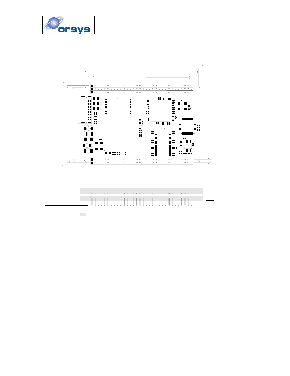
H
ARDWARE REFERENCE GUIDE
MICRO-LINE
C6713CPU
Date : 28 November 2005
Doc. no. : C6713CPU_HRG
Iss./Rev : 1.1
Page : 50
7.9 Dimensions of the Board
Figure 12 shows the dimensions of the C6713CPU. When the C6713CPU is stacked with other
modules, board spacing is 14mm.
C9
78.74
90.17
97.54
58.42
60.96
67.06
2.54
2.54
1,5
1,5
6,0
5,0
3,5
maximum heigh of components
Figure 12: Dimensions of the C6713CPU (in millimeters)
In case of a customized carrier design, it is recommended to reserve some more space additionally
to the existing micro-line
®
connectors of the C6713CPU. This space does not necessarily need to
be mounted with connectors. It is only recommended not to place components into this region. This
allows to mount micro-line
®
peripheral boards and/or future micro-line® processor boards in the
same socket. The full micro-line footprint is listed below. Recommended keep-out areas are
connector rows A, B, BB, C, D, E for CPU boards and A, B, BB, C, D, E, EGND 1..4, P, X1..X10 for
peripheral boards. Rows EE, 1394-1, 1394-2, EGND5 and X11..16 are very unlikely to be used
and can therefore be used for placing components.
Page 51
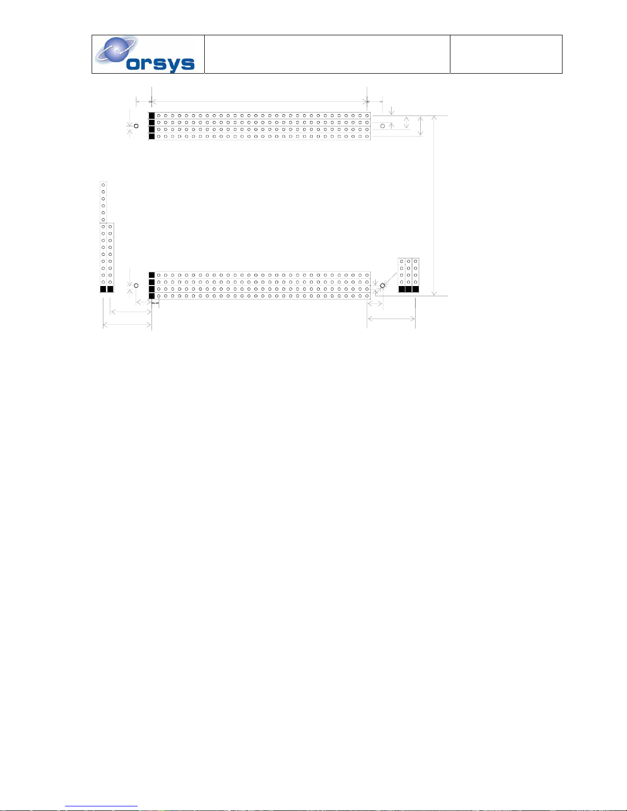
H
ARDWARE REFERENCE GUIDE
MICRO-LINE
C6713CPU
Date : 28 November 2005
Doc. no. : C6713CPU_HRG
Iss./Rev : 1.1
Page : 51
2.54
5.71
1.27
5.71
15,24
17.78
5.71
5.71
17.78
2.54
5.08
7.62
2.5
1.27
B
AA
A
BB
XP
E
C
D
EE
1394-2
1394-1
EGND
16
10
1
1
32
1
5
1
32
1,27
66,04
78,74
Figure 13: Complete micro-line® footprint
Page 52
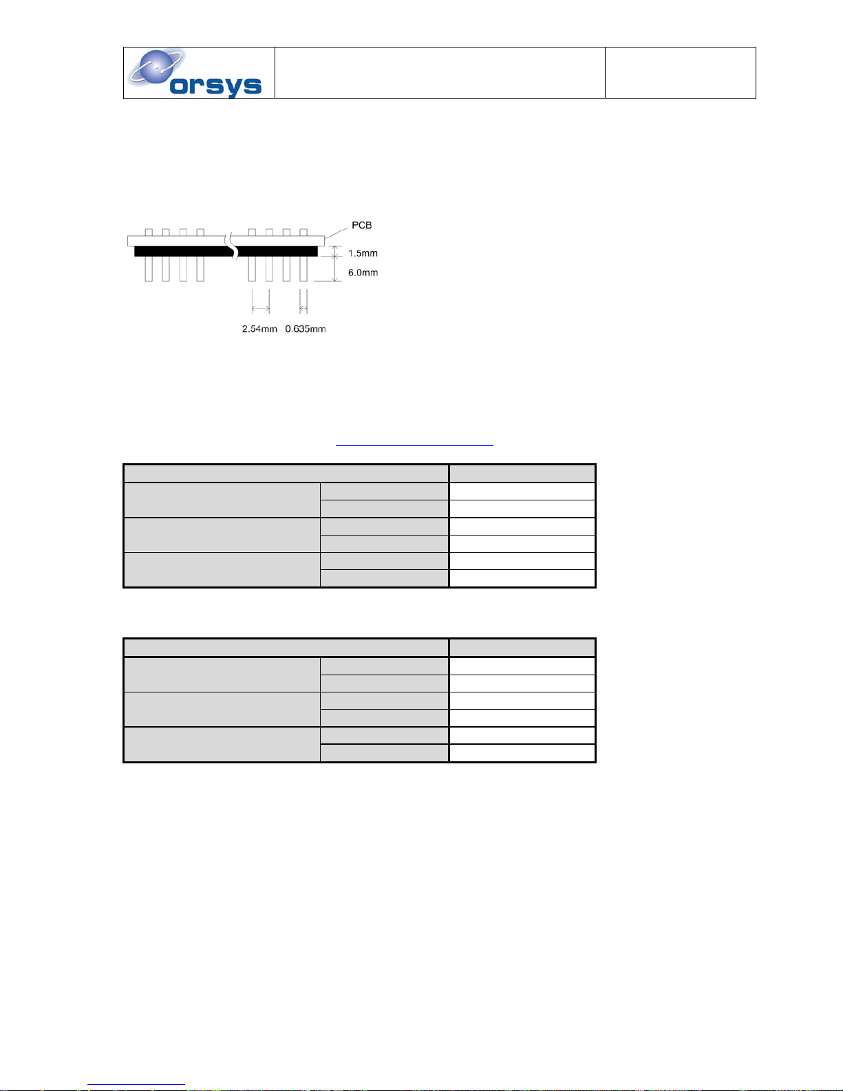
H
ARDWARE REFERENCE GUIDE
MICRO-LINE
C6713CPU
Date : 28 November 2005
Doc. no. : C6713CPU_HRG
Iss./Rev : 1.1
Page : 52
7.10 Spare micro-line® Connectors
The C6713CPU uses square connectors with 0.1 inch (2.54 mm) spacing. In contrast to previous
micro-line
®
CPU boards, the C6713CPU does not allow stacking other boards on top of it.
However, peripheral boards are stackable.
Figure 14: C6713CPU connector pins
The tables below give part number examples for spare micro-line connectors that can be used to
build customized carrier boards or peripheral boards.
Manufacturer: fischer Elektronik,
www.fischerelektronik.de
xx = number of pins, 1..32 for single row, 2..64 for double row
Connector type Part. No.
single row SL LP 1 112 xx G CPU board, not stackable
double row SL LP 2 112 xx G
single row BL1 xx or BL 5 xx Carrier board, not stackable
double row BL 2 xx or BL 6 xx
single row n/a peripheral board, stackable
double row n/a
Manufacturer: Preci-DIP, www.precidip.ch
xx = number of pins, 1..32 for single row, 2..64 for double row
Connector type Part. No.
single row n/a CPU board, not stackable
double row n/a
single row 801-pp-xx-10-001001 Carrier board, not stackable
double row 803-pp-xx-10-001001
single row 801-pp-xx-53-001001 peripheral board, stackable
double row 803-pp-xx-53-001001
Page 53

H
ARDWARE REFERENCE GUIDE
MICRO-LINE
C6713CPU
Date : 28 November 2005
Doc. no. : C6713CPU_HRG
Iss./Rev : 1.1
Page : 53
8 List of abbreviations used in this document
BSP board support package: a combination of software and FPGA design that provides
further functionality to the C6713CPU
CCS
Code Composer Studio –TI's development environment
CPU
Central Processing Unit = processor
DMA
direct memory access – a fast data transfer method
DSP Digital Signal Processor
e.g.
exempli gratia (Latin) = for example
yEMI
electromagnetic interference
EMIF
external memory interface – a peripheral of the TMS320C6713 DSP
FPGA
field programmable gate array
HPI
host port interface – a peripheral of the TMS320C6713 DSP
i.e.
id est (Latin) = that is
I
2
C inter integrated circuit – a low speed interface between integrated circuits
KB 1024 byte
LED
light emitting diode
LSB least significant bit
MB 1024 KB = 1048576 byte
MSB
most significant bit
McASP
multi-channel audio serial port – a peripheral of the TMS320C6713 DSP
McBSP
multi-channel buffered serial port – a peripheral of the TMS320C6713 DSP
N.A.
not available / not applicable
N.C.
not connected
PLD
programmable logic device
RAM
random access memory
ROM
read only memory
SRAM
static random access memory
SDRAM
synchronous dynamic random access memory
TBC
to be changed = value not 100% tested and may change in future
TBD
to be defined = value is not yet specified
TI
Texas Instruments
UART
universal asynchronous receiver transmitter
Page 54
H
ARDWARE REFERENCE GUIDE
MICRO-LINE
C6713CPU
Date : 28 November 2005
Doc. no. : C6713CPU_HRG
Iss./Rev : 1.1
Page : 54
9 Literature references
Further information that is not covered in this user's guide can be found in the documents listed
below. References to this list are given in square brackets throughout this document. The
documents are listed by title, author and literature number or file name
[1] Texas Instruments website at
www.ti.com
[2] Xilinx website at
www.xilinx.com
[3]
TMS320C6000 Technical Brief
, TI,
SPRU197
[4]
TMS320C6713 floating-point digital signal processor data sheet
, TI,
SPRS186
[5]
TMS320C6000 CPU and instruction set reference
, TI,
SPRU189
[6]
TMS320C6000 peripherals reference guide
, TI,
SPRU190
[7]
TMS320C6000 DSP Multichannel Audio Serial Port (McASP) Reference Guide
, TI,
SPRU041
[8]
TMS320C6000 DSP Software-Programmable Phase-Locked Loop (PLL) Controller Reference
Guide
, TI,
SPRU233
[9]
TMS320C6000 DSP Inter-Integrated Circuit (I2C) Module Reference Guide
, TI,
SPRU175
[10]
TMS320C6713 Errata Sheet
, TI,
SPRZ191
[11]
Manual Update Sheet for TMS320C6000 Peripherals Reference Guide (SPRU190)
, TI,
SPRZ122
[12] application report "
Applications Using the TMS320C6000 Enhanced DMA
", TI,
SPRA636
[13] application report "
TMS320C621x/TMS320C671x EDMA Queue Management Guidelines
", TI,
SPRA720
[14]
How to Begin Development Today With the TMS320C6713 Floating-Point DSP
, TI,
SPRA809
[15]
Optimizing C-Compiler user's guide
, TI,
SPRU187
[16]
TMS320C6000 Assembly Language Tools User’s Guide
, TI,
SPRU186
[17]
TMS320C62x/C67x Programmer’s Guide
, TI,
SPRU198
[18]
TMP100 temperature sensor data sheet
, TI,
SBOS231
[19]
MX29LV160CT/CB 16 Megabit Flash Memory
, Macronix,
PM1186
[20]
C6713CPU DSP Development Kit User’s Guide
, Orsys,
C6713CPU_DSP_DevKit_ug
[21]
C6713CPU micro-line Busmaster Board Support Package
, Orsys,
®
C6713CPU_ML_BM_ug
[22]
C6713CPU FPGA Programming Guide
, Orsys,
C6713CPU_FPGA_pg
[23]
Power Supply Board
, Orsys,
power_supply
[24]
Flash File System User's Guide
, Orsys,
FFS_ug
 Loading...