

OPTREX DMF-51026NYU-LY Datasheet
DMF-51026NYU-LY (AA) No.2000-0179 OPTREX CORPORATION Page 1/18
OPTREX
Type No.
*******
May 1, 2000
First Edition
Final Revision
Quality Assurance Div.
Production Div.
Checked by
Checked by
Approved by
Production Div.
Design Engineering Div.
Prepared by
LCD Module Specification
DMF-51026NYU-LY
DMF-51026NYU-LYDMF-51026NYU-LY
DMF-51026NYU-LY
Table of Contents
1. General Specifications .............................................................................2
2. Electrical Specifications...........................................................................3
3. Optical Specifications..............................................................................8
4. I/O Terminal...........................................................................................10
5. Test..........................................................................................................12
6. Appearance Standards............................................................................13
7. Code System of Production Lot ..........................................................16
8. Type Number..........................................................................................16
9. Applying Precautions .............................................................................16
10. Precautions Relating Product Handling................................................17
11. Warranty..................................................................................................18
Revision History
Rev. Date Page Comment
DMF-51026NYU-LY (AA) No.2000-0179 OPTREX CORPORATION Page 2/18
OPTREX
1.General Specifications
Operating Temp.
:
min. 0℃ ~ max. 50℃
Storage Temp.
:
min. -20℃ ~ max. 60℃
Dot Pixels
:
160 (W) × 64 (H) dots
Dot Size
:
0.34 (W) × 0.34 (H) mm
Dot Pitch
:
0.37 (W) × 0.37 (H) mm
Viewing Area
:
62.4 (W) × 27.6 (H) mm
Outline Dimensions
:
89.0 (W) × 35.6 (H) × 13.9* max. (D) mm
* Without I/O Connecter
W eight
:
60g max.
LCD Type
:
NTD-12641
( STN / Yellow-mode / Transmissive )
Viewing Angle
:
12:00
Data Transfer
:
4-bit parallel data transfer
Backlight
:
LED Backlight / Yellow-green
Drawings
:
Dimensional Outline UE-300215
DMF-51026NYU-LY (AA) No.2000-0179 OPTREX CORPORATION Page 3/18
OPTREX
2.Electrical Specifications
2.1.Absolute Maximum Ratings
V
SS
=0V
Parameter Symbol Conditions Min. Max. Units
Supply Voltage
(Logic)
VCC-VSS
-
-0.3 7.0 V
Supply Voltage
(LCD Drive)
VCC-VEE
-
0 30.0 V
Input Voltage VI
-
-0.3 VCC+0.3 V
2.2.DC Characteristics
Ta=25℃, V
SS
=0V
Parameter Symbol Conditions Min. Typ. Max. Units
Supply Voltage
(Logic)
VCC-VSS
-
4.5 - 5.5 V
VCC-VEE
-
15.6 - 17.4 V
Supply Voltage
(LCD Drive)
V
CC-VADJ
Shown in 3.1 V
High Level
Input Voltage
VIH VCC=5.0V±10% 0.7×VCC
-
V
CC
V
Low Level
Input Voltage
VIL VCC=5.0V±10% 0 - 0.3×VCC V
Supply Current
ICC VCC-VSS=5.0V
-
0.9 0.4 mA
I
EE
VCC-VEE=13.5V
-
0.8 1.2 mA
DMF-51026NYU-LY (AA) No.2000-0179 OPTREX CORPORATION Page 4/18
OPTREX
2.3.AC Characteristics
V
CC
=5.0V±10%
Parameter Symbol Min. Max. Units
Clock Pulse Cycle Time
t
CYC
125 - ns
Clock Pulse Hi gh Level Width
t
CWH
40 - ns
Clock Pulse Low Level Width
t
CWL
40 - ns
Clock Pulse Setup Time
t
SCL
80 - ns
Clock Pulse Hold Time
t
HCL
80 - ns
Clock Pulse Rise/Fall Time
t
r, tf
-
Note1 ns
LP High Level Width
t
LWH
80 - ns
LP Low Level Width
t
LWL
1.0 -
μ
s
LP Cycle Time
t
CL1
10 -
μ
s
Data Setup Time
t
DS
20 - ns
Data Hold Time
t
DH
20 - ns
FLM Data Setup Time
t
FS
100 - ns
FLM Data Hold Time
t
FH
100 - ns
M Phase Difference
t
CM
-
300 ns
Note1:Please satisfy the following conditions (1),(2) in the same time.
(1)
t
r, tf < (
t
CYC - tCWH - tCWL
)/2
(2)
t
r, tf ≦ 50
t
FH
t
FS
t
r
t
f
t
DH
t
DS
t
CWL
t
HCL
t
SCL
CP
LP
M
FLM
D0~D3
t
LWH
t
CYC
t
CWH
t
CM
t
LWL
t
CL1
t
r
t
f
DMF-51026NYU-LY (AA) No.2000-0179 OPTREX CORPORATION Page 5/18
OPTREX
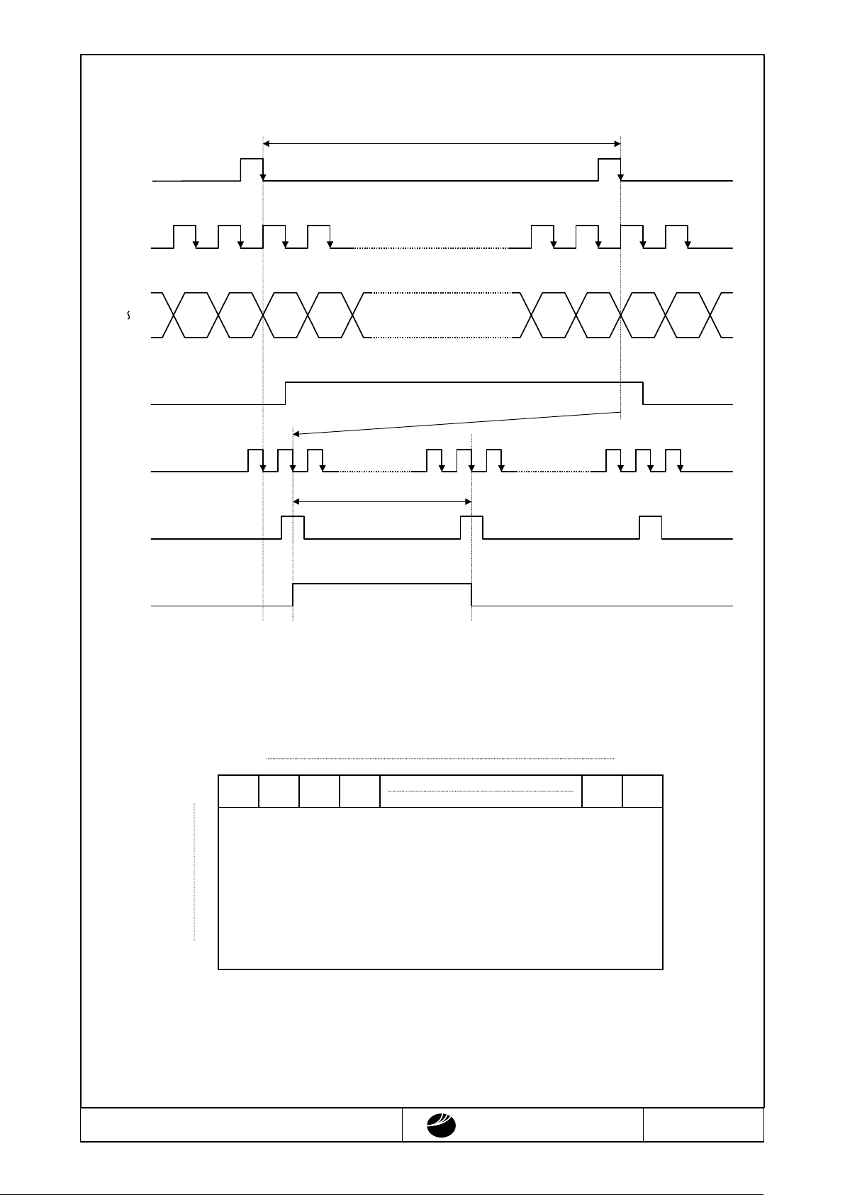
2.4.Timing Chart
2.5.Comparison of Display and Data
T=0.187ms typ.
64×T
FLM
LP
FLM
M
D3
D0
CP
LP
~
#1 DATA
SEGSEG SEGSEG SEGSEG SEGSEG
160156 84160156 84
157
~
153
~
5
~
1
~
157
~
153
~
5
~
1
~
(Reduction)
(Reduction)
SEG1 SEG160
#1
#64
D2D3
D0~D3
TOP VIEW
D0D1 D0D1
DMF-51026NYU-LY (AA) No.2000-0179 OPTREX CORPORATION Page 6/18
OPTREX
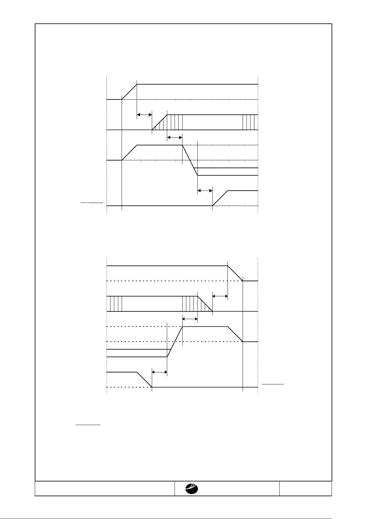
2.6.Power Supply ON/OFF Sequence
2.6.1.ON Sequence
2.6.2.OFF Sequence
Please maintain the above sequence when turning on and off the power supply of the module.
If DISPOFF is supplied to the module
w
hile internal alternate signal for LCD driving (M) is
unstable, DC component will be supplied to the LCD panel. This may cause damage the LCD
module.
VCC
VSS
VEE
VSS
VSS
VCC
VSS
DISPOFF
VCC
VCC
VEE
0≦t
SIGNAL
0≦t
SIGNAL
VCC
LEVEL
0≦t
VADJ
VADJ
VCC
VSS
VEE
VSS
VSS
VCC
VSS
DISPOFF
VCC
VCC
VEE
0≦t
SIGNAL
0≦t
SIGNAL
VCC
LEVEL
0≦t
VADJ
VADJ
 Loading...