

OPTREX DMF-50961NF-SFW Datasheet
DMF-50961NF-SFW (AB) No.99-0053 OPTREX CORPORATION Page 1/18
OPTREX
Type No.
*******
Mar 8, 1999
First Edition
Final Revision
Quality Assurance Div.
Production Div.
Checked by
Checked by
Approved by
Production Div.
Design Engineering Div.
Prepared by
LCD Module Specification
DMF-50961NF-SFW
DMF-50961NF-SFWDMF-50961NF-SFW
DMF-50961NF-SFW
Table of Contents
1. General Specifications .............................................................................2
2. Electrical Specifications...........................................................................3
3. Optical Specifications..............................................................................8
4. I/O Terminal...........................................................................................10
5. Test..........................................................................................................12
6. Appearance Standards............................................................................13
7. Code System of Production Lot ..........................................................16
8. Type Number..........................................................................................16
9. Applying Precautions .............................................................................16
10. Precautions Relating Product Handling................................................17
11. Warranty..................................................................................................18
Revision History
Rev. Date Page Comment
DMF-50961NF-SFW (AB) No.99-0053 OPTREX CORPORATION Page 2/18
OPTREX
1.General Specifications
Operating Temp.
:
min. 0℃ ~ max. 50℃
Storage Temp.
:
min. -20℃ ~ max. 60℃
Dot Pixels
:
640×480 (H) dots
Dot Size
:
0.21 (W) × 0.21 (H) mm
Dot Pitch
:
0.23 (W) × 0.23 (H) mm
Viewing Area
:
153.0 (W) × 115.4 (H) mm
Outline Dimensions
:
201.0
*
(W) × 141.0 (H) × 6.5 max. (D) mm
* Without CFL Cable and mounting holes.
W eight
:
230g max.
LCD Type
:
NTD-12708
(F-STN / Black
&White-mode / Transflective )
Viewing Angle
:
6:00
Data Transfer
:
4-bit parallel data transfer × 2
Backlight
:
Cold Cathode Fluorescent Lamp (CFL) × 1
Drawings
:
Dimensional Outline UE-300170A
DMF-50961NF-SFW (AB) No.99-0053 OPTREX CORPORATION Page 3/18
OPTREX
2.Electrical Specifications
2.1.Absolute Maximum Ratings
V
SS
=0V
Parameter Symbol Conditions Min. Max. Units
Supply Voltage
(Logic)
VCC-VSS
-
-0.3 7.0 V
Supply Voltage
(LCD Drive)
VHH-VSS
-
-0.3 32.0 V
Input Voltage VI
-
-0.3 VCC+0.3 V
2.2.DC Characteristics
Ta=25℃, V
SS
=0V
Parameter Symbol Conditions Min. Typ. Max. Units
Supply Voltage
(Logic)
VCC-VSS
-
2.5 - 5.5 V
Supply Voltage
(LCD Drive)
VHH-VSS Shown in 3.1 V
High Level
Input Voltage
VIH VCC=2.5~5.5V 0.8×VCC
-
V
CC
V
Low Level
Input Voltage
VIL VCC=2.5~5.5V 0 - 0.2×VCC V
Supply Current
ICC VCC-VSS=5.0V
-
2.0 5.0 mA
I
HH
VHH-VSS=21.8V
-
7.0 20.0 mA
DMF-50961NF-SFW (AB) No.99-0053 OPTREX CORPORATION Page 4/18
OPTREX
2.3.AC Characteristics
V
CC
=2.5~5.5V
Parameter Symbol Min. Max. Units
Clock Pulse Cycle Time
t
WCK
152 - ns
Clock Pulse Hi gh Level Width
t
WCKH
65 - ns
Clock Pulse Low Level Width
t
WCKL
65 - ns
Latch Pulse High Level Width
t
WLPH
65 - ns
CP→LP Rise Time
t
LD
0 - ns
CP→LP Fall Time
t
SL
65 - ns
LP→CP Rise Time
t
LS
65 - ns
LP→CP Fall Time
t
LH
65 - ns
Clock Pulse Rise/Fall Time
t
r, tf 50 ns
Data Setup Time
t
DS
50 - ns
Data Hold Time
t
DH
40 - ns
DISPOFF Low Level Width
t
WDL
1.2 -
μ
s
DISPOFF Cancellation Time
t
SD
100 - ns
t
WDL
t
SD
t
r
t
f
t
DH
t
DS
t
WCKL
t
LH
t
SL
CP
t
LD
t
LS
LP
DISPOFF
D0~D3
t
WLPH
TOP DATALAST DATA
t
WCK
t
WCKH
DMF-50961NF-SFW (AB) No.99-0053 OPTREX CORPORATION Page 5/18
OPTREX
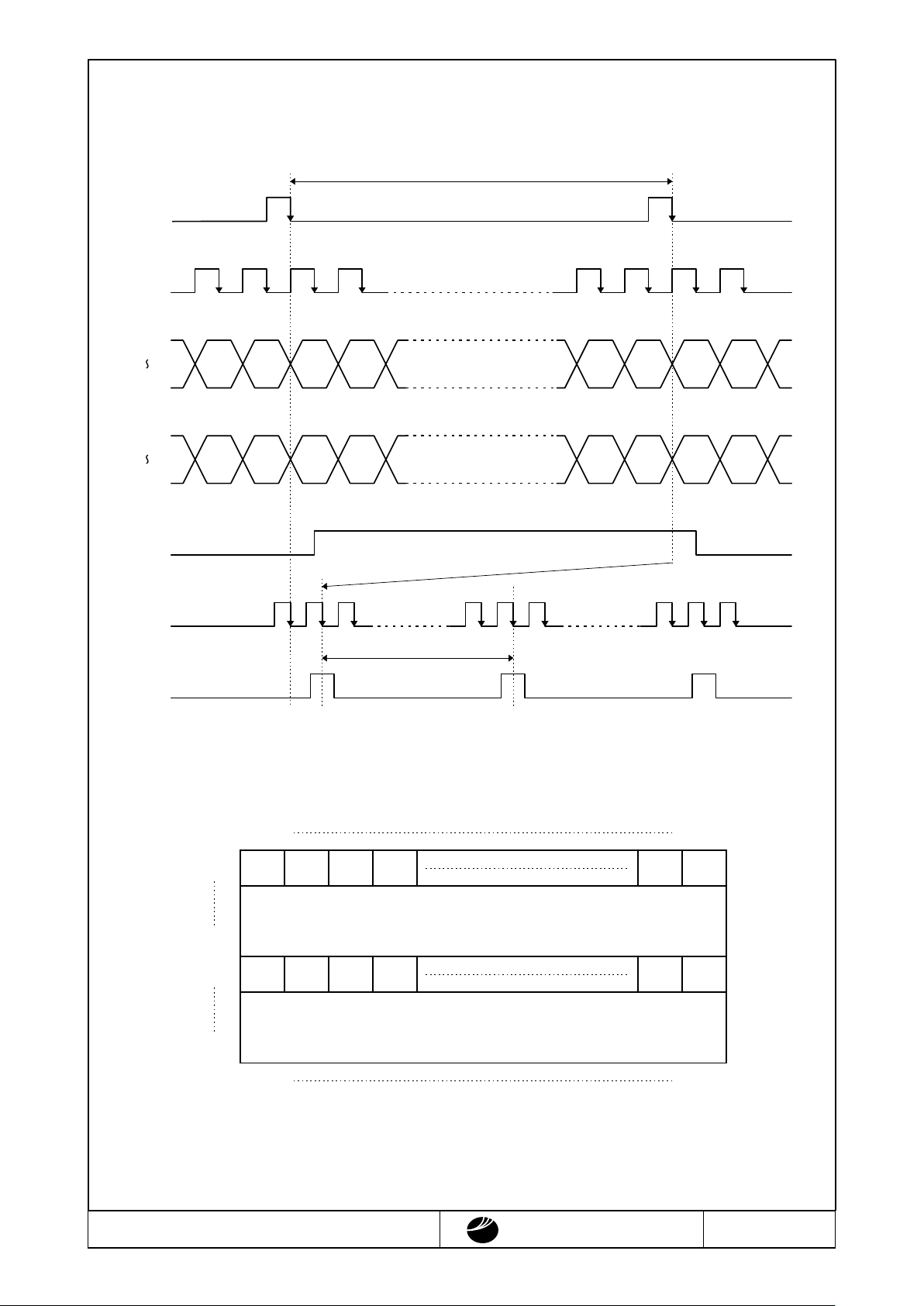
2.4.Timing Chart
2.5.Comparison of Display and Data
T=0.0595ms typ.
240×T
FLM
(
reduction
)
(
reduction
)
LP
FLM
DU3
DU0
CP
LP
~
#1 DATA
SEGSEG SEGSEG SEGSEG SEGSEG
640636 84640636 84
637
~
633
~
5
~
1
~
637
~
633
~
5
~
1
~
DL3
DL0
~
#241 DATA
SEGSEG SEGSEG SEGSEG SEGSEG
12801276 648644 12801276 648644
1277
~
1273
~
645
~
641
~
1277
~
1273
~
645
~
641
~
SEG1 SEG640
#241
#1
#240
#480
DU2DU3
DU0~DU3
DL0~DL3
SEG641 SEG1280
DU0DU1 DU0DU1
DL2DL3 DL0DL1 DL0DL1
DMF-50961NF-SFW (AB) No.99-0053 OPTREX CORPORATION Page 6/18
OPTREX
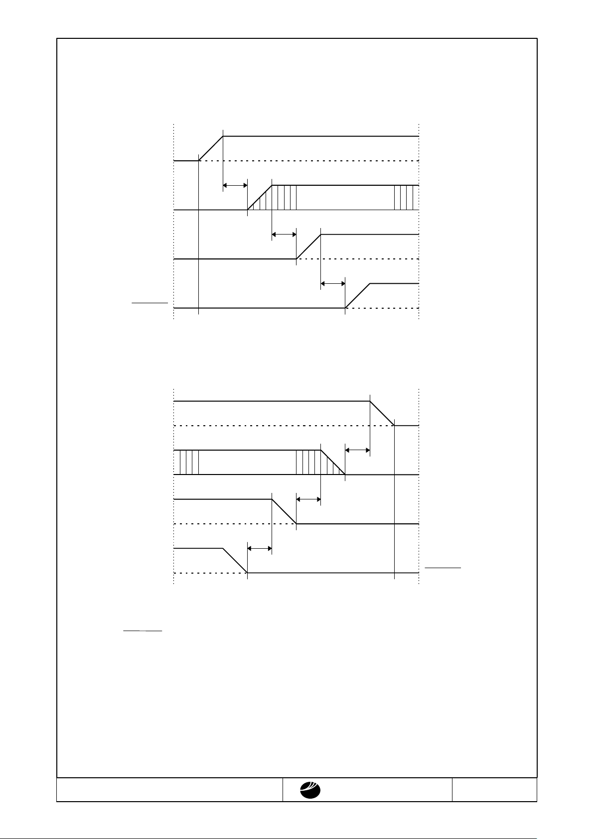
2.6.Power Supply ON/OFF Sequence
2.6.1.ON Sequence
2.6.2.OFF Sequence
Please maintain the above sequence when turning on and off the power supply of the module.
If DISPOFF is supplied to the module
w
hile internal alternate signal for LCD driving (M) is
unstable, DC component will be supplied to the LCD panel. This may cause damage the LCD
module.
VSS
VCC
VSS
VSS
VCC
VSS
VCC
DISPOFF
VHH
VCC
0≦t
0≦t
SIGNAL
SIGNAL
LEVEL
VHH
0≦t
VSS
VCC
VSS
VSS
VCC
VSS
VCC
DISPOFF
VHH
VCC
0≦t
0≦t
SIGNAL
SIGNAL
LEVEL
VHH
0≦t
 Loading...