

OPTREX DMF-50807NFH-T Datasheet
DMF-50807NFH-T (AB) No.2000-0169 OPTREX CORPORATION Page 1/17
OPTREX
Type No.
*******
Apr 26, 2000
First Edition
Final Revision
Quality Assurance Div.
Production Div.
Checked by
Checked by
Approved by
Production Div.
Design Engineering Div.
Prepared by
LCD Module Specification
DMF-50807NFH-T
DMF-50807NFH-TDMF-50807NFH-T
DMF-50807NFH-T
Table of Contents
1. General Specifications .............................................................................2
2. Electrical Specifications...........................................................................3
3. Optical Specifications..............................................................................5
4. I/O Terminal.............................................................................................9
5. Test..........................................................................................................11
6. Appearance Standards............................................................................12
7. Code System of Production Lot ..........................................................15
8. Type Number..........................................................................................15
9. Applying Precautions .............................................................................15
10. Precautions Relating Product Handling................................................16
11. Warranty..................................................................................................17
Revision History
Rev. Date Page Comment

DMF-50807NFH-T (AB) No.2000-0169 OPTREX CORPORATION Page 2/17
OPTREX
1.General Specifications
Operating Temp.
:
min. -20℃ ~ max. 70℃
Storage Temp.
:
min. -30℃ ~ max. 80℃
Dot Pixels
:
248 (W) × 60 (H) dots
Dot Size
:
0.36 (W) × 0.32 (H) mm
Dot Pitch
:
0.38 (W) × 0.34 (H) mm
Viewing Area
:
99.0 (W) × 25.0 (H) mm
Outline Dimensions
:
123.0 (W) × 97.0 (H) × 2.9* max. (D) mm
* Without Parts Height
W eight
:
38g max.
LCD Type
:
NTD-15780
( F-STN / Black
&White-mode / Transmissive )
Viewing Angle
:
6:00
Data Transfer
:
8-bit parallel data transfer
Backlight
:
None
Drawings
:
Dimensional Outline UE-36912C
DMF-50807NFH-T (AB) No.2000-0169 OPTREX CORPORATION Page 3/17
OPTREX
2.Electrical Specifications
2.1.Absolute Maximum Ratings
V
SS
=0V
Parameter Symbol Conditions Min. Max. Units
Supply Voltage
(Logic)
VDD-VSS
-
-0.3 7.0 V
Input Voltage VI
-
-0.3 VDD+0.3 V
2.2.DC Characteristics
Ta=25℃, V
SS
=0V
Parameter Symbol Conditions Min. Typ. Max. Units
Supply Voltage
(Logic)
VDD-VSS
-
4.5 - 5.5 V
High Level
Input Voltage
VIH VDD=5.0V±10% 0.7×VDD
-
V
DD
V
Low Level
Input Voltage
VIL VDD=5.0V±10% 0 - 0.3×VDD V
High Level
Output Voltage
VOH IOH=-1.0mA 0.8×VDD
-
V
DD
V
Low Level
Output Voltage
VOL IOL=1.0mA 0 - 0.2×VDD V
Supply Current IDD VDD-VSS=5.0V
-
2.0 5.0 mA
DMF-50807NFH-T (AB) No.2000-0169 OPTREX CORPORATION Page 4/17
OPTREX
2.3.AC Characteristics
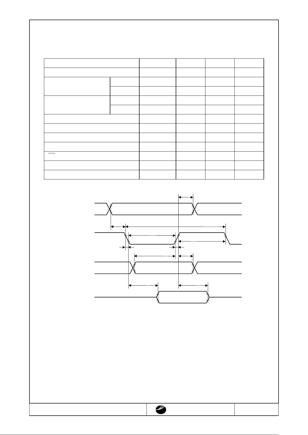
2.3.1.Read/Write Operation Sequence (80 series CPU)
V
DD
=5.0V±10%
Parameter Symbol Min. Max. Units
System Cycle Time
t
CYC8
200 - ns
Control High P ul s e Width READ
t
CCHR
117 - ns
WRITE
t
CCHW
172 - ns
Control Low Pulse Width READ
t
CCLR
77 - ns
WRITE
t
CCLW
22 - ns
Address Setup Time
t
AW8
10 - ns
Address Hold Time
t
AH8
10 - ns
Data Setup Time
t
DS8
20 - ns
Data Hold Time
t
DH8
10 - ns
RD Access Time
t
ACC8
-
70 ns
Output Disable Time
t
OH8
10 50 ns
Input Signal Change Time
t
r, tf
-
15 ns
(READ)
(WRITE)
D0~D7
D0~D7
(/CSIM,/CSIS)
/WR, /RD
t
ACC8
t
OH8
t
AH8
t
DH8
t
r
t
f
t
DS8
t
AW8
t
CCLR
,
t
CCLW
t
CYC8
A0
t
CCHR
,
t
CCHW
DMF-50807NFH-T (AB) No.2000-0169 OPTREX CORPORATION Page 5/17
OPTREX
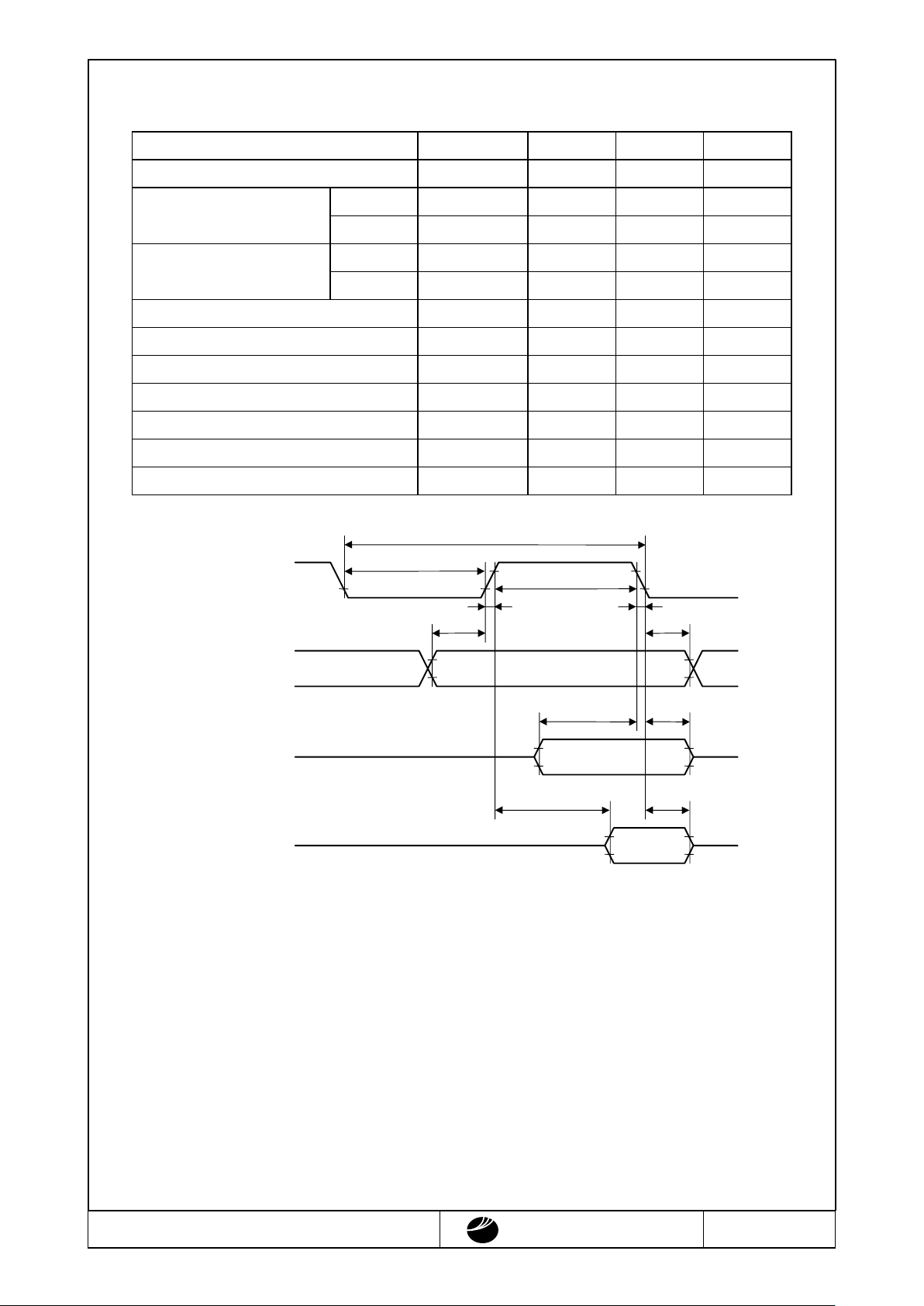
2.3.2.Read/Write Operation Sequence (68 series CPU)
V
DD
=5.0V±10%
Parameter Symbol Min. Max. Units
System Cycle Time
t
CYC6
200 - ns
Enable High Pulse Width READ
t
EWHR
77 - ns
WRITE
t
EWHW
22 - ns
Enable Low Pulse Width READ
t
EWLR
117 - ns
WRITE
t
EWLW
172 - ns
Address Setup Time
t
AW6
10 - ns
Address Hold Time
t
AH6
10 - ns
Data Setup Time
t
DS6
20 - ns
Data Hold Time
t
DH6
10 - ns
Access Time
t
ACC6
-
70 ns
Output Disable Time
t
OH6
10 50 ns
Input Signal Change Time
t
r, tf
-
15 ns
(READ)
(WRITE)
D0~D7
D0~D7
A0, R/W
t
ACC6
t
OH6
t
DH6
t
DS6
t
CYC6
E, (/CSIM,/CSIS)
t
AH6
t
f
t
r
t
AW6
t
EWHR
,
t
EWHW
t
EWLR
,
t
EWLW
DMF-50807NFH-T (AB) No.2000-0169 OPTREX CORPORATION Page 6/17
OPTREX
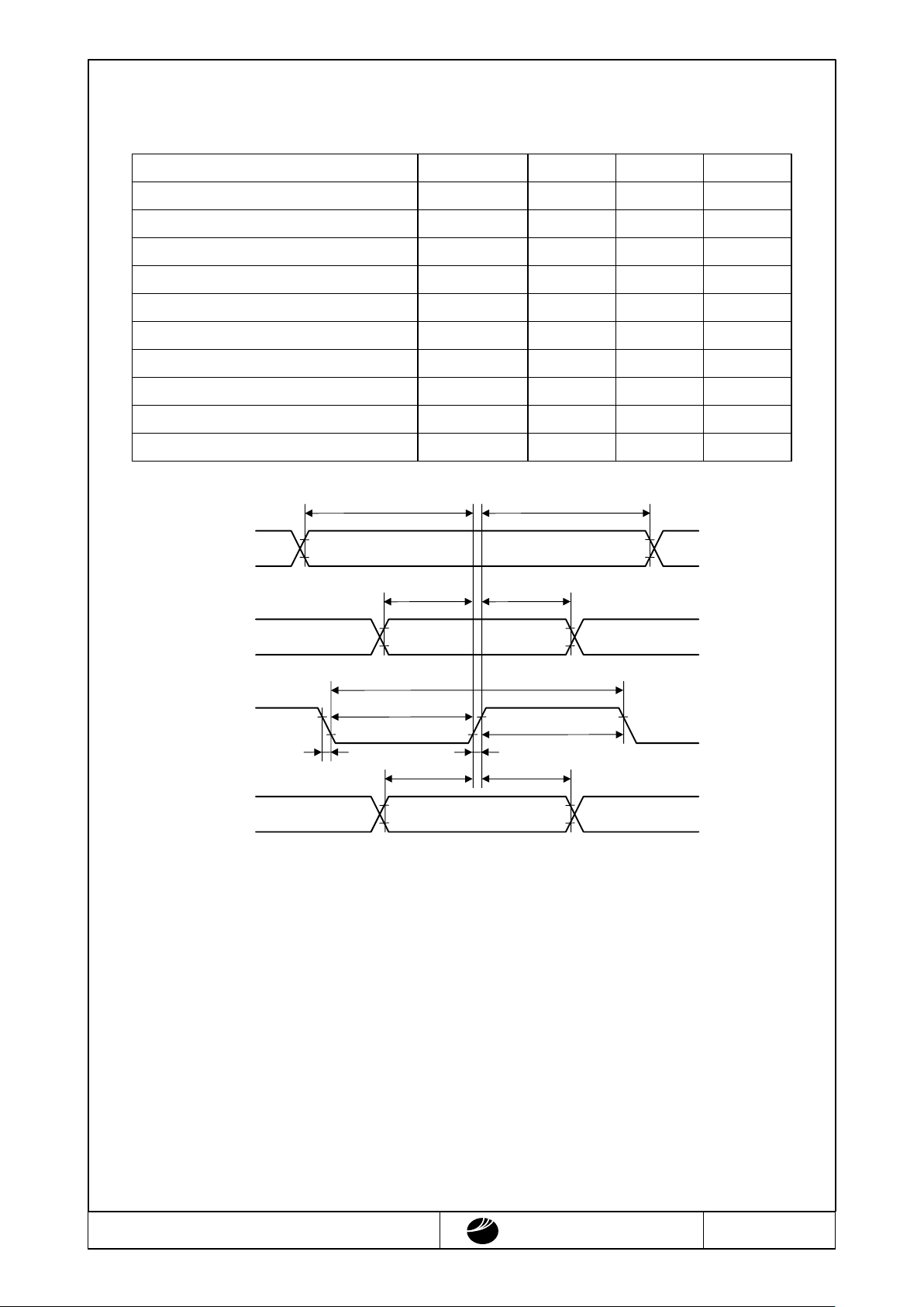
2.3.3.Serial Interface Sequence
V
DD
=5.0±10%
Parameter Symbol Min. Max. Units
Serial Clock Cycle Time
t
SCYC
500 - ns
Serial Clock High Pulse Width
t
SHW
150 - ns
Serial Clock Low Pulse Width
t
SLW
150 - ns
Address Setup Time
t
SAS
120 - ns
Address Hold Time
t
SAH
200 - ns
Data Setup Time
t
SDS
120 - ns
Data Hold Time
t
SDH
50 - ns
Chip Select Setup Time
t
CSS
30 - ns
Chip Select Hold Time
t
CSH
400 - ns
Input Signal Change Time
t
r, tf
-
15 ns
SI
SCL
A0
t
CSH
t
CSS
/CSIM,/CSIS
t
SHW
t
SLW
t
SCYC
t
SAS
t
SAH
t
SDH
t
r
t
f
t
SDS
 Loading...