

OPTREX DMF-50773NB-FW Datasheet
LCD Module Specification
First Edition
Apr 27, 1999
Final Revision
*******
Approved by
Checked by
Checked by
Production Div.
Quality Assurance Div.
Design Engineering Div.
Type No.
DMF-50773NB-FW
DMF-50773NB-FW
DMF-50773NB-FWDMF-50773NB-FW
Table of Contents
Prepared by
1. General Specifications .............................................................................2
2. Electrical Specifications...........................................................................3
3. Optical Specifications..............................................................................7
4. I/O Terminal.............................................................................................9
5. Test..........................................................................................................11
6. Appearance Standards............................................................................12
7. Code System of Production Lot ..........................................................15
8. Type Number..........................................................................................15
9. Applying Precautions .............................................................................15
10. Precautions Relating Product Handling................................................16
11. Warranty..................................................................................................17
Revision History
Rev. Date Page Comment
Production Div.
DMF-50773NB-FW (AG) No.99-0083 OPTREX CORPORATION Page 1/17
OPTREX
1. General Specifications
Operating Temp.
Storage Temp.
Dot Pixels
Dot Size
Dot Pitch
Viewing Area
Outline Dimensions
W eight
LCD Type
Viewing Angle
Control LSI
Data Transfer
Backlight
Drawings
min. 0℃ ~ max. 50℃
:
min. -20℃ ~ max. 60℃
:
240 (W) × 128 (H) dots
:
0.47 (W) × 0.47 (H) mm
:
0.50 (W) × 0.50 (H) mm
:
126.0 (W) × 70.0 (H) mm
:
170.0 (W) × 105.0* (H) × 14.0 max. (D) mm
:
* Without CFL Cable
250g max.
:
NTD-15524
:
( STN / Blue-mode / Transmissive )
6:00
:
T6963C-0101 (Produced by TOSHIBA)
:
8-bit parallel data transfer
:
Cold Cathode Fluorescent Lamp (CFL) × 1
:
Dimensional Outline UE-36773
:
DMF-50773NB-FW (AG) No.99-0083 OPTREX CORPORATION Page 2/17
OPTREX
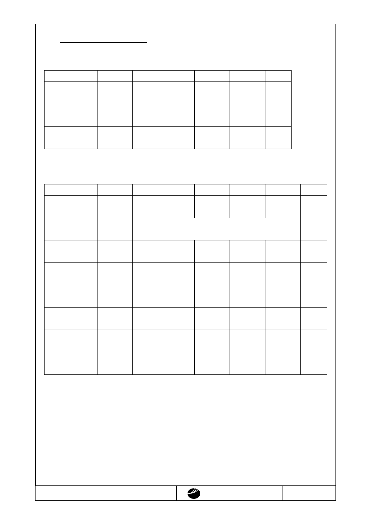
2.Electrical Specifications
2.1.Absolute Maximum Ratings
Parameter Symbol Conditions Min. Max. Units
GND=0V
Supply Voltage
(Logic)
Supply Voltage
(LCD Drive)
Input Voltage VI
2.2.DC Characteristics
Parameter Symbol Conditions Min. Typ. Max. Units
Supply Voltage
(Logic)
Supply Voltage
(LCD Drive)
High Level
Input Voltage
VDD-GND
VDD-VEE
-0.3 7.0 V
-
-0.3 30.0 V
-
-0.3 VDD+0.3 V
-
Ta=25℃, GND=0V
VDD-GND
4.5 - 5.5 V
-
VDD-VEE Shown in 3.1 V
VIH VDD=5.0V±10% VDD-2.2
V
-
V
DD
Low Level
VIL VDD=5.0V±10% 0 - 0.8 V
Input Voltage
High Level
VOH IOH=-0.75mA VDD-0.3
Output Voltage
Low Level
VOL IOL=0.75mA 0 - 0.3 V
Output Voltage
IDD VDD-GND=5.0V
Supply Current
I
VDD-VEE=18.5V
EE
V
-
9.0 14.0 mA
-
2.9 4.5 mA
-
V
DD
DMF-50773NB-FW (AG) No.99-0083 OPTREX CORPORATION Page 3/17
OPTREX
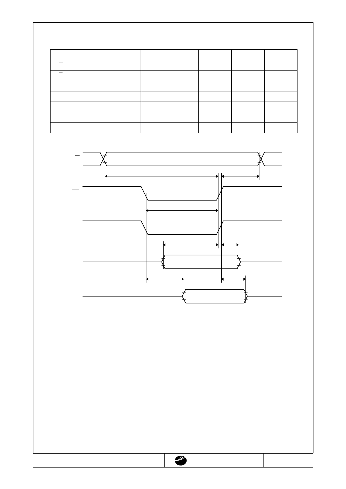
2.3.AC Characteristics
Parameter Symbol Min. Max. Units
=5.0V±10%
V
DD
C/D Setup Time
C/D Hold Time
CE, RD, WR Pulse Width
Data Setup Time
Data Hold Time
Access Time
Output Hold Time
t
100 - ns
CDS
t
10 - ns
CDH
t
t
t
,
,
CE
t
t
t
t
ACC
80 - ns
RD
WR
80 - ns
DS
40 - ns
DH
10 50 ns
OH
150 ns
-
C/D
CDS
t
CDH
t
CE
CE
RD
WR
,
,
t
t
t
RD, WR
DS
t
DH
t
D0~D7
(WRITE)
ACC
t
OH
t
D0~D7
(READ)
DMF-50773NB-FW (AG) No.99-0083 OPTREX CORPORATION Page 4/17
OPTREX
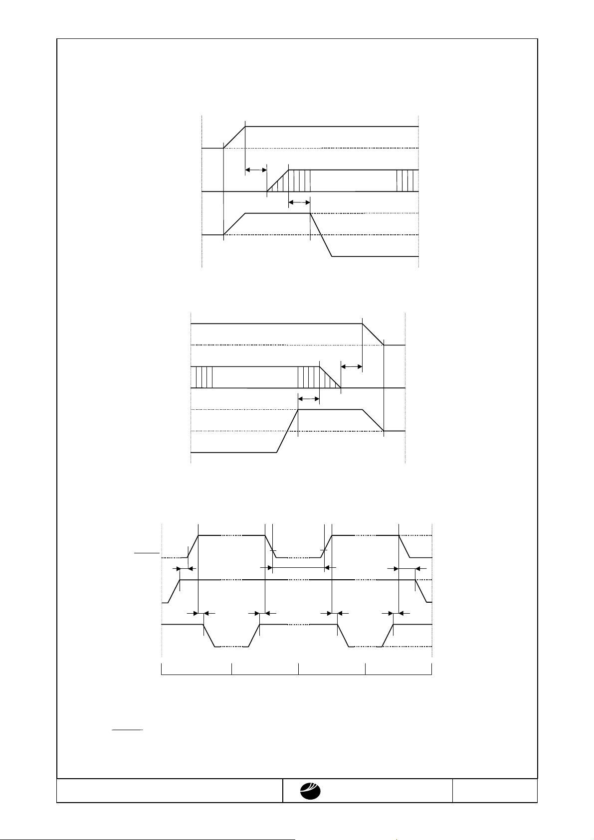
2.4.Power Supply ON/OFF Sequence
2.4.1.ON Sequence
(Without RESET Signal)
SIGNAL
VDD
SIGNAL
VEE
0≦t
0≦t
LEVEL
VDD
GND
VDD
GND
VDD
GND
VEE
2.4.2.OFF Sequence
LEVEL
VDD
GND
VDD
GND
VDD
GND
0≦t
0≦t
SIGNAL
VDD
SIGNAL
(Without RE S E T Signal)
VEE
VEE
2.4.3.Reset Sequence
SIGNAL
LEVEL
RESET
T>250μs
T≧10 ms
T≧0
VDD
VEE
T≧0T≧0T≧50msT≧50ms
H Level
L Level
VDD
GND
VDD
Power OffPower On Reset CancellationReset
VEE
Please maintain the above sequence when turning on and off the power supply of the module.
If V
is supplied to the module while internal alternate signal for LCD driving (M) is unstable or
EE
RESET is active, DC component will be supplied to the LCD panel. This may cause damage to
the LCD module.
DMF-50773NB-FW (AG) No.99-0083 OPTREX CORPORATION Page 5/17
OPTREX
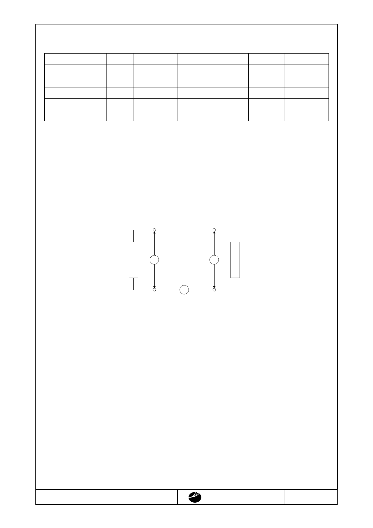
2.5.Lighting Specifications
Ta=25℃
Parameter Symbol Conditions Min. Typ. Max. Units Notes
Lamp Voltage VL
Lamp Current IL
Starting Voltage VS
Surface Luminance L IL=5.0mA 100 -
Average Life TAL I
-
4.0 5.0 6.0 mArms 2
-
450 -
-
=5.0mA
L
350 - Vrms 1
-
Vrms 3
-
cd/㎡ 4
-
15000 - hrs 5
-
Note 1 : The voltage ( r.m.s. ) to maintain the electric discharge of the lamp. It is measured after lighting for
3 minutes .
Note 2 : The current ( r.m.s. ) to flow through the lamp with the electric discharge. It i s mea s ured after
lighting for 3 minutes .
Note 3 : The voltage at starting the electric discharge when the voltage is increased gradually from 0V.
Note 4 : Surface Luminance is specified by the initial data of luminance measured at the center of display
surface after 20 minutes power on. ( All ON pattern )
Note 5 : CFL life is defined as the time for which the initial luminance is attenuated by 50% of the
luminance value. Average Life representes the time elapsed at the point of time when the residual
ratio becomes below 50% when plural lamps are lighted in comparison with the definition of life
mentioned above.
I
N
V
VS VL
C
F
L
CFL Testing Circuit
IL
Recommended Inverter : S-12565 ( Produced by ELEVAM ) CXA-M10A (DC 5.0V, Produced by TDK)
CXA-M10L (DC 12.0V, Produced by TDK)
DMF-50773NB-FW (AG) No.99-0083 OPTREX CORPORATION Page 6/17
OPTREX
 Loading...