

OPTREX DMF-50427NJ-SLY Datasheet
DMF-50427NJ-SLY (AB) No.99-0111 OPTREX CORPORATION Page 1/18
OPTREX
Type No.
*******
May 1, 1999
First Edition
Final Revision
Quality Assurance Div.
Production Div.
Checked by
Checked by
Approved by
Production Div.
Design Engineering Div.
Prepared by
LCD Module Specification
DMF-50427NJ-SLY
DMF-50427NJ-SLYDMF-50427NJ-SLY
DMF-50427NJ-SLY
Table of Contents
1. General Specifications .............................................................................2
2. Electrical Specifications...........................................................................3
3. Optical Specifications..............................................................................8
4. I/O Terminal...........................................................................................10
5. Test..........................................................................................................12
6. Appearance Standards............................................................................13
7. Code System of Production Lot ..........................................................16
8. Type Number..........................................................................................16
9. Applying Precautions .............................................................................16
10. Precautions Relating Product Handling................................................17
11. Warranty..................................................................................................18
Revision History
Rev. Date Page Comment

DMF-50427NJ-SLY (AB) No.99-0111 OPTREX CORPORATION Page 2/18
OPTREX
1. General Specifications
Operating Temp.
:
min. -20℃ ~ max. 70℃
Storage Temp.
:
min. -20℃ ~ max.70℃
Dot Pixels
:
128 (W) × 64 (H) dots
Dot Size
:
0.40 (W) × 0.40 (H) mm
Dot Pitch
:
0.43 (W) × 0.43 (H) mm
Viewing Area
:
60.0 (W) × 32.5 (H) mm
Outline Dimensions
:
75.0 (W) × 52.7 (H) × 8.5 max. (D) mm
W eight
:
50g max.
LCD Type
:
NSD-13051
( STN / Neutral-mode / Transflective )
Viewing Angle
:
6:00
Data Transfer
:
8-bit parallel data transfer
Backlight
:
LED Backlight / Yellow-green
Drawings
:
Dimensional Outline UE-35372B
DMF-50427NJ-SLY (AB) No.99-0111 OPTREX CORPORATION Page 3/18
OPTREX
2.Electrical Specifications
2.1.Absolute Maximum Ratings
V
SS
=0V
Parameter Symbol Conditions Min. Max. Units
Supply Voltage
(Logic)
VDD-VSS
-
-0.3 7.0 V
Supply Voltage
(LCD Drive)
VDD-VLC
-
-0.3 17.0 V
Input Voltage VI
-
-0.3 VDD+0.3 V
2.2.DC Characteristics
Ta=25℃, V
SS
=0V
Parameter Symbol Conditions Min. Typ. Max. Units
Supply Voltage
(Logic)
VDD-VSS
-
4.5 - 5.5 V
Supply Voltage
(LCD Drive)
VDD-VLC Shown in 3.1 V
High Level
V
IH1
VDD=5.0V±10%
Note 1
0.7×VDD
-
V
DD
V
Input Voltage V
IH2
VDD=5.0V±10%
Note 2
2.0
-
V
DD
V
Low Level
V
IL1
VDD=5.0V±10%
Note 1
0
-
0.3×VDD V
Input Voltage V
IL2
VDD=5.0V±10%
Note 2
0
-
0.8 V
High Level
Output Voltage
VOH IOH=-0.205mA
V
DD
=5.0V±10%
2.4
-
-
V
Low Level
Output Voltage
VOL IOL=1.2mA
V
DD
=5.0V±10%
-
-
0.4 V
Supply Current
IDD VDD-VSS=5.0V
-
2.1 5.0 mA
I
LC
VDD-VLC=13.1V
-
1.8 4.0 mA
Note 1 : Apply to RST
Note 2 : Apply to DB0~DB7, CS1, CS2, R/W, D/I, E
DMF-50427NJ-SLY (AB) No.99-0111 OPTREX CORPORATION Page 4/18
OPTREX
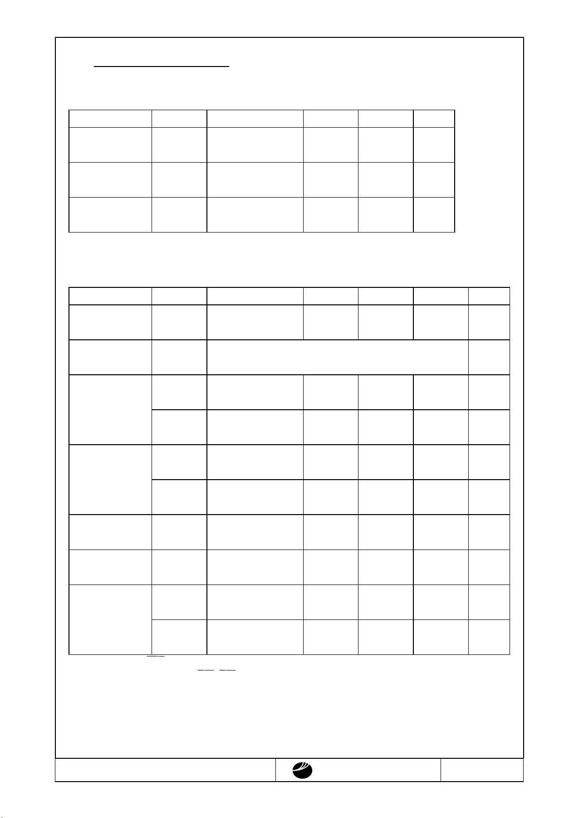
2.3.AC Characteristics
2.3.1.Timing Characteristics
V
DD
=5.0V±10%
Parameter Symbol Conditions Min. Max. Units
Enable Cycle Time
t
CYC
Fig.1, 2 1000 - ns
Enable Pulse Width PW
EH,
PWEL Fig.1, 2 450
-
ns
Enable Rise/Fall Time
t
E
r,
t
E
f Fig.1, 2 - 25 ns
Address Setup Time
t
AS
Fig.1, 2 140 - ns
Address Hold Time
t
AH
Fig.1, 2 10 - ns
Write Data Setup Time
t
DSW
Fig.1 200 - ns
Write Data Hold Time
t
DHW
Fig.1 10 - ns
Read Data Delay Time
t
DDR
Fig.2 - 320 ns
Read Data Hold Time
t
DHR
Fig.2 20 - ns
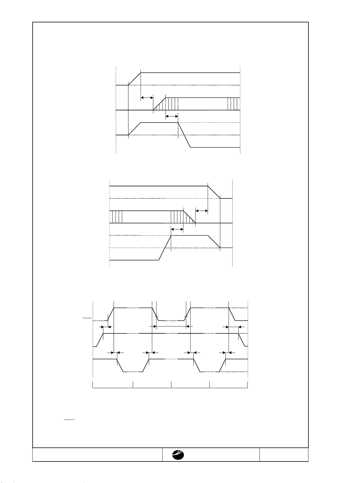
Fig.1 Write Operation Timing
Fig.2 Read Operation Timing
E
R/W
V
IL
V
IH
t
CYC
PW
EH
V
IL
t
E
r
t
E
f
t
DSW
t
DHW
t
AH
t
AS
V
IL
Valid Data
D/I
DB0~DB7
V
IH
V
IL
V
IH
V
IL
V
IH
V
IL
V
IL
V
IH
V
IL
V
IH
V
IL
PW
EL
E
R/W
V
IH
V
IH
V
IH
PW
EH
t
DDR
t
E
f
t
CYC
t
DHR
t
E
r
t
AH
t
AS
V
IL
D/I
DB0~DB7
Valid Data
V
IH
V
IL
V
IH
V
IL
V
IH
V
IL
V
IL
V
OH
V
OL
V
OH
V
OL
PW
EL
DMF-50427NJ-SLY (AB) No.99-0111 OPTREX CORPORATION Page 5/18
OPTREX
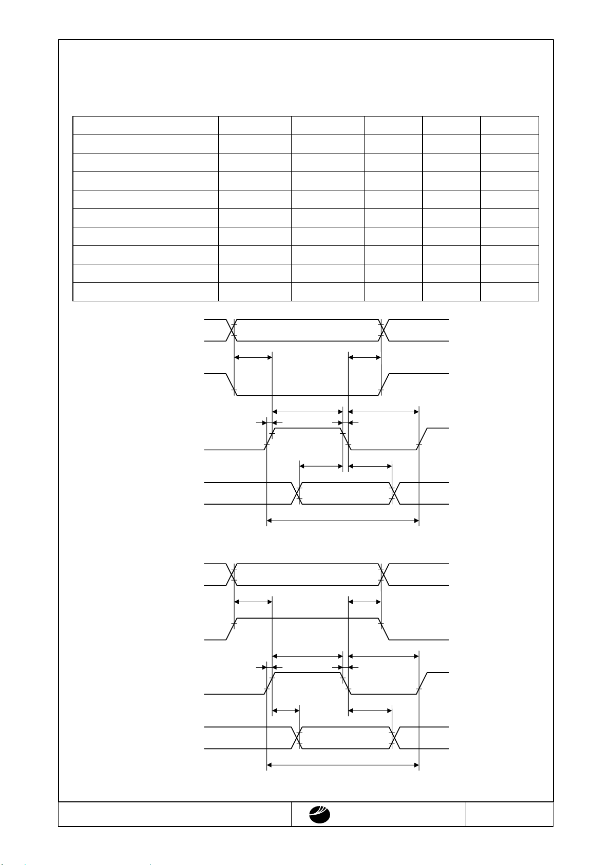
2.3.2.Power Supply Initial Conditions
Parameter Symbol Min. Max. Units
Reset Low Level Time
t
RST
1.0 -
μ
s
Reset Rise Time
t
r
-
200 ns
Do not fail to set the system again because RESET during operation may destroy the data in
all the registers except ON/OFF register and in RAM.
RST
VDD
t
RST
t
r
DMF-50427NJ-SLY (AB) No.99-0111 OPTREX CORPORATION Page 6/18
OPTREX
2.4.Power Supply ON/OFF Sequence
2.4.1.ON Sequence
2.4.2.OFF Sequence
2.4.3.Reset Sequence
Please maintain the above sequence when turning on and off the power supply of the module.
If V
LC
is supplied to the module while internal alternate signal for LCD driving (M) is unstable or
RST is active, DC component will be supplied to the LCD panel. This may cause damage to the
LCD module.
RST
VDD
VLC
SIGNAL
T≧0
T≧0T≧0T≧50msT≧50ms
T>250μs
LEVEL
L Level
H Level
VDD
VLC
VDD
VSS
Power OffPower On Reset CancellationReset
T≧10 ms
VLC
VSS
VSS
VDD
VSS
VDD
VLC
VDD
0≦t
0≦t
SIGNAL
SIGNAL
LEVEL
VDD
(Without RESET Signal)
VLC
VSS
VSS
VDD
VSS
VDD
VLC
VDD
0≦t
0≦t
SIGNAL
SIGNAL
LEVEL
VDD
(Without RE S E T Signal)
 Loading...