

OPTREX DMF-50202NYJ-SLY Datasheet
DMF-50202NYJ-SLY (AE) No.99-0152 OPTREX CORPORATION Page 1/18
OPTREX
Type No.
*******
May 28, 1999
First Edition
Final Revision
Quality Assurance Div.
Production Div.
Checked by
Checked by
Approved by
Production Div.
Design Engineering Div.
Prepared by
LCD Module Specification
DMF-50202NYJ-SLY
DMF-50202NYJ-SLYDMF-50202NYJ-SLY
DMF-50202NYJ-SLY
Table of Contents
1. General Specifications .............................................................................2
2. Electrical Specifications...........................................................................3
3. Optical Specifications..............................................................................8
4. I/O Terminal...........................................................................................10
5. Test..........................................................................................................12
6. Appearance Standards............................................................................13
7. Code System of Production Lot ..........................................................16
8. Type Number..........................................................................................16
9. Applying Precautions .............................................................................16
10. Precautions Relating Product Handling................................................17
11. Warranty..................................................................................................18
Revision History
Rev. Date Page Comment
DMF-50202NYJ-SLY (AE) No.99-0152 OPTREX CORPORATION Page 2/18
OPTREX
1. General Specifications
Operating Temp.
:
min. -20℃ ~ max. 70℃
Storage Temp.
:
min. -30℃ ~ max. 80℃
Dot Pixels
:
128 (W) × 64 (H) dots
Dot Size
:
0.40 (W) × 0.56 (H) mm
Dot Pitch
:
0.44 (W) × 0.60 (H) mm
Viewing Area
:
62.0 (W) × 44.0 (H) mm
Outline Dimensions
:
95.0 (W) × 58.0 (H) × 15.5 max. (D) mm
W eight
:
80g max.
LCD Type
:
NSD-7496
( STN / Yellow-mode / Transflective )
Viewing Angle
:
6:00
Data Transfer
:
Serial data transfer
Backlight
:
LED Backlight / Yellow-green
Drawings
:
Dimensional Outline UE-34641D
DMF-50202NYJ-SLY (AE) No.99-0152 OPTREX CORPORATION Page 3/18
OPTREX
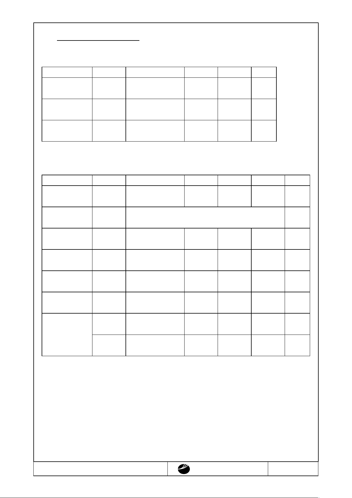
2.Electrical Specifications
2.1.Absolute Maximum Ratings
V
SS
=0V
Parameter Symbol Conditions Min. Max. Units
Supply Voltage
(Logic)
VDD-VSS
-
-0.3 7.0 V
Supply Voltage
(LCD Drive)
VDD-VEE
-
0 30.0 V
Input Voltage VI
-
-0.3 VDD+0.3 V
2.2.DC Characteristics
Ta=25℃, V
SS
=0V
Parameter Symbol Conditions Min. Typ. Max. Units
Supply Voltage
(Logic)
VDD-VSS
-
4.5 - 5.5 V
Supply Voltage
(LCD Drive)
VDD-VEE Shown in 3.1 V
High Level
Input Voltage
VIH VDD=5.0V±10% VDD-0.8
-
V
DD
V
Low Level
Input Voltage
VIL VDD=5.0V±10% 0 - 0.8 V
High Level
Output Voltage
VOH IOH=-0.5mA VDD-0.5
-
V
DD
V
Low Level
Output Voltage
VOL IOL=0.5mA 0 - 0.5 V
Supply Current
IDD VDD-VSS=5.0V
-
1.0 1.8 mA
I
EE
VDD-VEE=14.7V
-
0.8 1.4 mA
DMF-50202NYJ-SLY (AE) No.99-0152 OPTREX CORPORATION Page 4/18
OPTREX
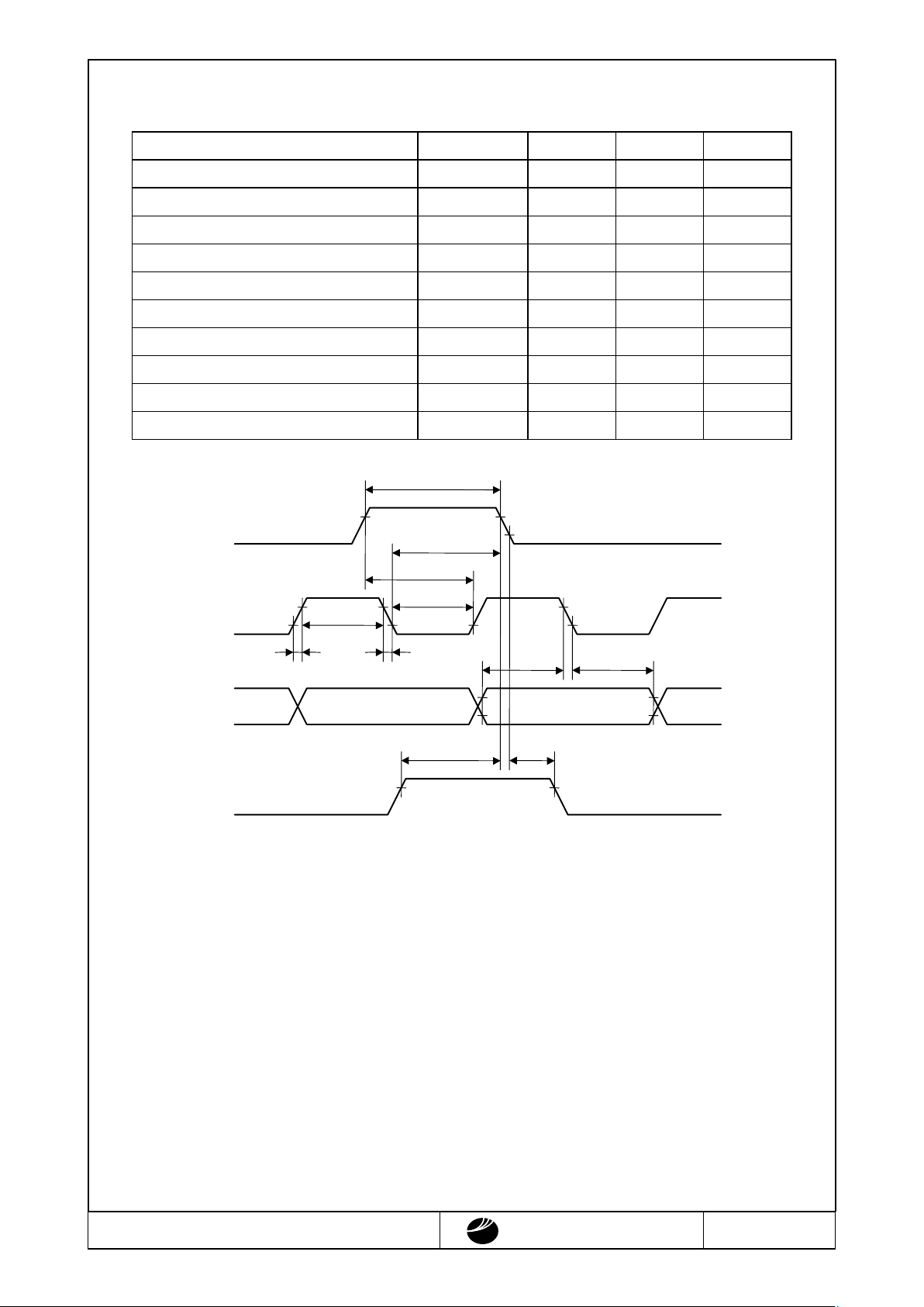
2.3.AC Characteristics
V
DD
=5.0V±10%
Parameter Symbol Min. Max. Units
Clock Pulse Hi gh Level Width
t
CWH
95 - ns
Clock Pulse Low Level Width
t
CWL
95 - ns
Clock Pulse Rise/Fall Time
t
r, tf
-
30 ns
Latch Pulse High Level Width
t
LW
40 - ns
Latch Pulse Rise Time
t
LRP
20 - ns
Latch Pulse Fall Time
t
LFP
40 - ns
Data Setup Time
t
DSU
20 - ns
Data Hold Time
t
DHD
40 - ns
FLM Data Setup Time
t
FDS
30 - ns
FLM Data Hold Time
t
FDH
50 - ns
t
FDH
t
FDS
t
r
t
f
t
DHD
t
DSU
t
CWL
t
LFP
CP2
t
LRP
CP1
FLM
D1
t
LW
t
CWH
DMF-50202NYJ-SLY (AE) No.99-0152 OPTREX CORPORATION Page 5/18
OPTREX
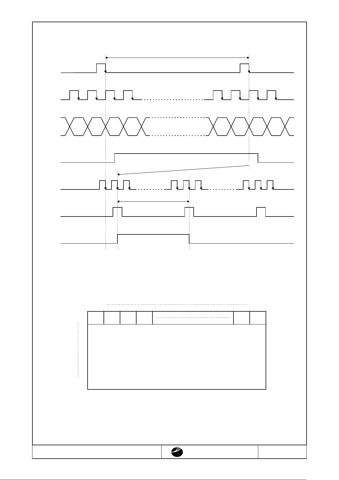
2.4.Timing Chart
2.5.Comparison of Display and Data
T=0.223ms typ.
64×T
FLM
(Reduction)
(Reduction)
CP1
FLM
M
D1
CP2
CP1
#1 DATA
SEGSEG SEGSEG SEGSEG SEGSEG
128127 21128127 21
SEG1 SEG128
#1
#64
D1D1
TOP VIEW
D1D1 D1D1
DMF-50202NYJ-SLY (AE) No.99-0152 OPTREX CORPORATION Page 6/18
OPTREX
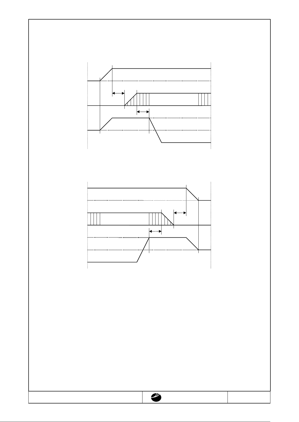
2.6.Power Supply ON/OFF Sequence
2.6.1.ON Sequence
2.6.2.OFF Sequence
Please maintain the above sequence when turning on and off the power supply of the module.
If V
EE
is supplied to the module while internal alternate signal for LCD driving (M) is unstable,
DC component will be supplied to the LCD panel. This may cause damage the LCD module.
VEE
VSS
VSS
VDD
VSS
VDD
VEE
VDD
0≦t
0≦t
SIGNAL
SIGNAL
LEVEL
VDD
VEE
VSS
VSS
VDD
VSS
VDD
VEE
VDD
0≦t
0≦t
SIGNAL
SIGNAL
LEVEL
VDD
 Loading...