

OPTREX DMF-50202N Datasheet

DMF-50202N (AA) No.97-0074 OPTREX CORPORATION Page 1/16
OPTREX
Type No.
*******
March 27, 1997
First Edition
Final Revision
Quality Assurance Div.
Production Div.
Checked by
Checked by
Approved by
Production Div.
Design Engineering Div.
Prepared by
LCD Module Specification
DMF-50202N
DMF-50202NDMF-50202N
DMF-50202N
Table of Contents
1. General Specifications.............................................................................2
2. Electrical Specifications...........................................................................3
3. Optical Specifications..............................................................................7
4. I/O Terminal.............................................................................................9
5. Test..........................................................................................................11
6. Appearance Standards............................................................................12
7. Code System of Production Lot..........................................................15
8. Type Number .........................................................................................15
9. Applying Precautions.............................................................................15
10. Handling Precautions.............................................................................16
Revision History
Rev. Date Page Comment
DMF-50202N (AA) No.97-0074 OPTREX CORPORATION Page 2/16
OPTREX
1.General Specifications
Operating Temp.
:
min. 0℃ ~ max. 50℃
Storage Temp.
:
min. -20℃ ~ max. 60℃
Dot Pixels
:
128 (W) × 64 (H) dots
Dot Size
:
0.40 (W) × 0.56 (H) mm
Dot Pitch
:
0.44 (W) × 0.60 (H) mm
Viewing Area
:
62.0 (W) × 44.0 (H) mm
Outline Dimensions
:
95.0 (W) × 58.0 (H) × 8.7 max. (D) mm
LCD Type
:
NRD-7496
( STN / Neutral-mode / Reflective )
Viewing Angle
:
6:00
Data Transfer
:
Serial data transfer
Backlight
:
None
Drawings
:
Dimensional Outline UE-33929A
DMF-50202N (AA) No.97-0074 OPTREX CORPORATION Page 3/16
OPTREX
2.Electrical Specifications
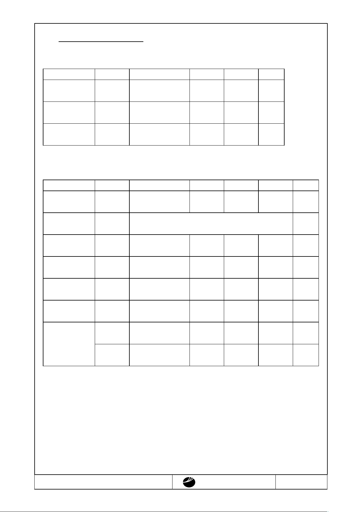
2.1.Absolute Maximum Ratings
V
SS
=0V
Parameter Symbol Conditions Min. Max. Units
Supply Voltage
(Logic)
VDD-VSS
-
-0.3 7.0 V
Supply Voltage
(LCD Drive)
VDD-VEE
-
0 30.0 V
Input Voltage VI
-
-0.3 VDD+0.3 V
2.2.DC Characteristics
Ta=25℃, V
SS
=0V
Parameter Symbol Conditions Min. Typ. Max. Units
Supply Voltage
(Logic)
VDD-VSS
-
4.5 - 5.5 V
Supply Voltage
(LCD Drive)
VDD-VEE Shown in 3.1 V
High Level
Input Voltage
VIH VDD=5.0V±10% VDD-0.8
-
V
DD
V
Low Level
Input Voltage
VIL VDD=5.0V±10% 0 - 0.8 V
High Level
Output Voltage
VOH IOH=-0.5mA VDD-0.3
-
V
DD
V
Low Level
Output Voltage
VOL IOL=0.5mA 0 - 0.3 V
Supply Current
IDD VDD-VSS=5.0V
-
1.0 1.5 mA
I
EE
VDD-VEE=13.2V
-
0.8 1.2 mA

DMF-50202N (AA) No.97-0074 OPTREX CORPORATION Page 4/16
OPTREX
2.3.AC Characteristics
V
DD
=5.0V±10%
Parameter Symbol Min. Max. Units
Clock Pulse Hi gh Level Width
t
CWH
95 - ns
Clock Pulse Low Level Width
t
CWL
95 - ns
Clock Pulse Rise/Fall Time
t
r, tf
-
30 ns
Latch Pulse High Level Width
t
LW
40 - ns
Latch Pulse Rise Time
t
LRP
20 - ns
Latch Pulse Fall Time
t
LFP
40 - ns
Data Setup Time
t
DSU
20 - ns
Data Hold Time
t
DHD
40 - ns
Frame Data Setup Time
t
FDS
30 - ns
Frame Data Hold Time
t
FDH
50 - ns
t
r
t
f
t
DSU
t
FDH
t
FDS
t
DHD
t
LRP
t
CWL
CP2
t
LFP
CP1
t
CWH
FLM
D1
t
LW
DMF-50202N (AA) No.97-0074 OPTREX CORPORATION Page 5/16
OPTREX
2.4.Timing Chart
2.5.Comparison of Display and Data
T=0.223ms typ.
64×T
FLM
(Reduction)
(Reduction)
CP1
FLM
M
D1
CP2
CP1
#1 DATA
SEGSEG SEGSEG SEGSEG SEGSEG
128127 21128127 21
SEG1 SEG128
#1
#64
D1D1
TOP VIEW
D1D1 D1D1
 Loading...