

OPTREX DMF-50174ZNB-FW Datasheet
LCD Module Specification
First Edition
Apr 25, 2000
Final Revision
*******
Approved by
Checked by
Checked by
Production Div.
Quality Assurance Div.
Design Engineering Div.
Type No.
DMF-50174ZNB-FW
DMF-50174ZNB-FW
DMF-50174ZNB-FWDMF-50174ZNB-FW
Table of Contents
Prepared by
1. General Specifications .............................................................................2
2. Electrical Specifications...........................................................................3
3. Optical Specifications..............................................................................8
4. I/O Terminal...........................................................................................10
5. Test..........................................................................................................12
6. Appearance Standards............................................................................13
7. Code System of Production Lot ..........................................................16
8. Type Number..........................................................................................16
9. Applying Precautions .............................................................................16
10. Precautions Relating Product Handling................................................17
11. Warranty..................................................................................................18
Revision History
Rev. Date Page Comment
Production Div.
DMF-50174ZNB-FW (AT) No.2000-0166 OPTREX CORPORATION Page 1/18
OPTREX
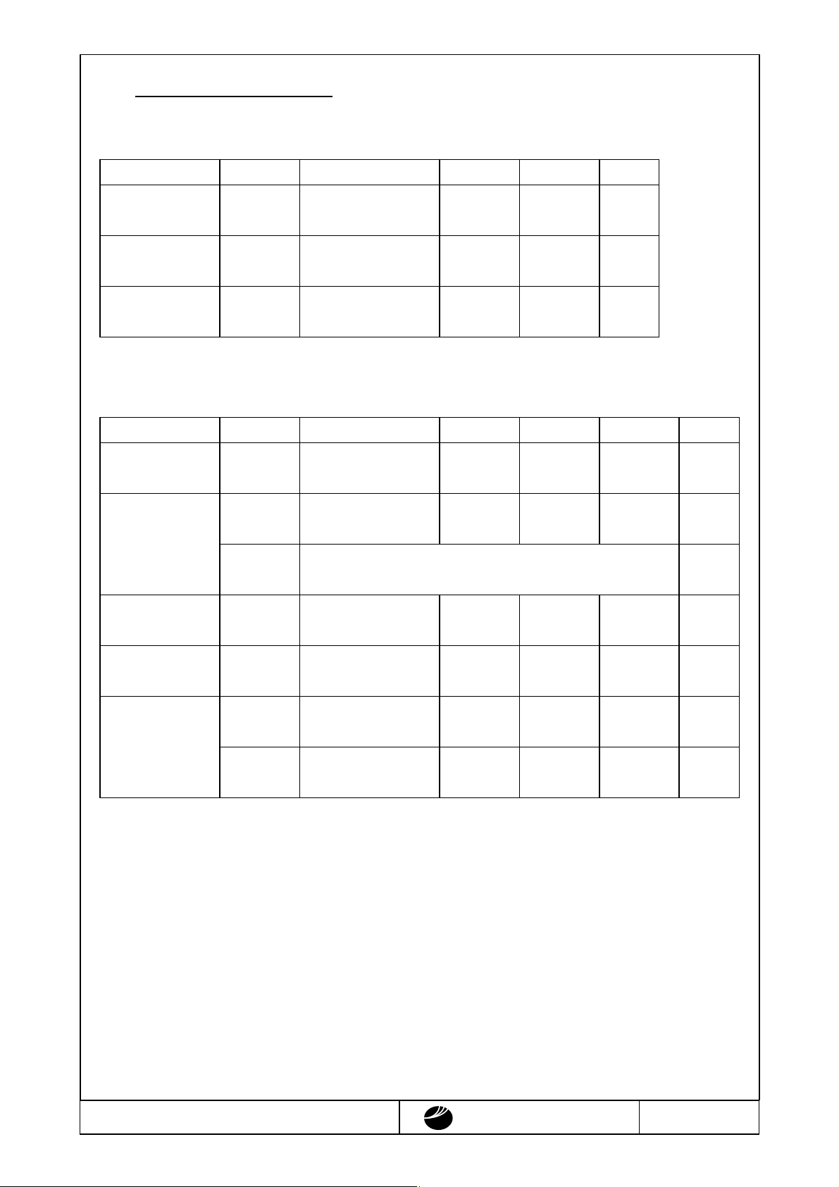
1.General Specifications
Operating Temp.
Storage Temp.
Dot Pixels
Dot Size
Dot Pitch
Viewing Area
Outline Dimensions
W eight
LCD Type
Viewing Angle
Data Transfer
Backlight
Drawings
min. 0℃ ~ max. 50℃
:
min. -20℃ ~ max. 60℃
:
320 (W) × 240 (H) dots
:
0.33 (W) × 0.33 (H) mm
:
0.36 (W) × 0.36 (H) mm
:
122.0 (W) × 92.0 (H) mm
:
*
:
174.0
(W) × 112.0 (H) × 14.0 max. (D) mm
* Without CFL Cable
300g max.
:
NTD-11437
:
( STN / Blue-mode / Transmissive )
6:00
:
4-bit parallel data transfer
:
Cold Cathode Fluorescent Lamp (CFL) × 1
:
Dimensional Outline UE-20762A
:
DMF-50174ZNB-FW (AT) No.2000-0166 OPTREX CORPORATION Page 2/18
OPTREX
2.Electrical Specifications
2.1.Absolute Maximum Ratings
Parameter Symbol Conditions Min. Max. Units
=0V
V
SS
Supply Voltage
(Logic)
Supply Voltage
(LCD Drive)
Input Voltage VI
2.2.DC Characteristics
Parameter Symbol Conditions Min. Typ. Max. Units
Supply Voltage
(Logic)
Supply Voltage
(LCD Drive) VCC-V
VCC-VSS
VCC-VEE
VCC-VSS
VCC-VEE
ADJ
-0.3 7.0 V
-
0 35.0 V
-
-0.3 VCC+0.3 V
-
Ta=25℃, V
4.5 - 5.5 V
-
27.1 - 32.0 V
-
SS
=0V
Shown in 3.1 V
High Level
VIH VCC=5.0V±10% 0.8×VCC
Input Voltage
Low Level
VIL VCC=5.0V±10% 0 - 0.2×VCC V
Input Voltage
ICC VCC-VSS=5.0V
Supply Current
I
VCC-V
EE
ADJ
=23.3V
V
-
6.0 15.0 mA
-
5.5 10.0 mA
-
V
CC
DMF-50174ZNB-FW (AT) No.2000-0166 OPTREX CORPORATION Page 3/18
OPTREX
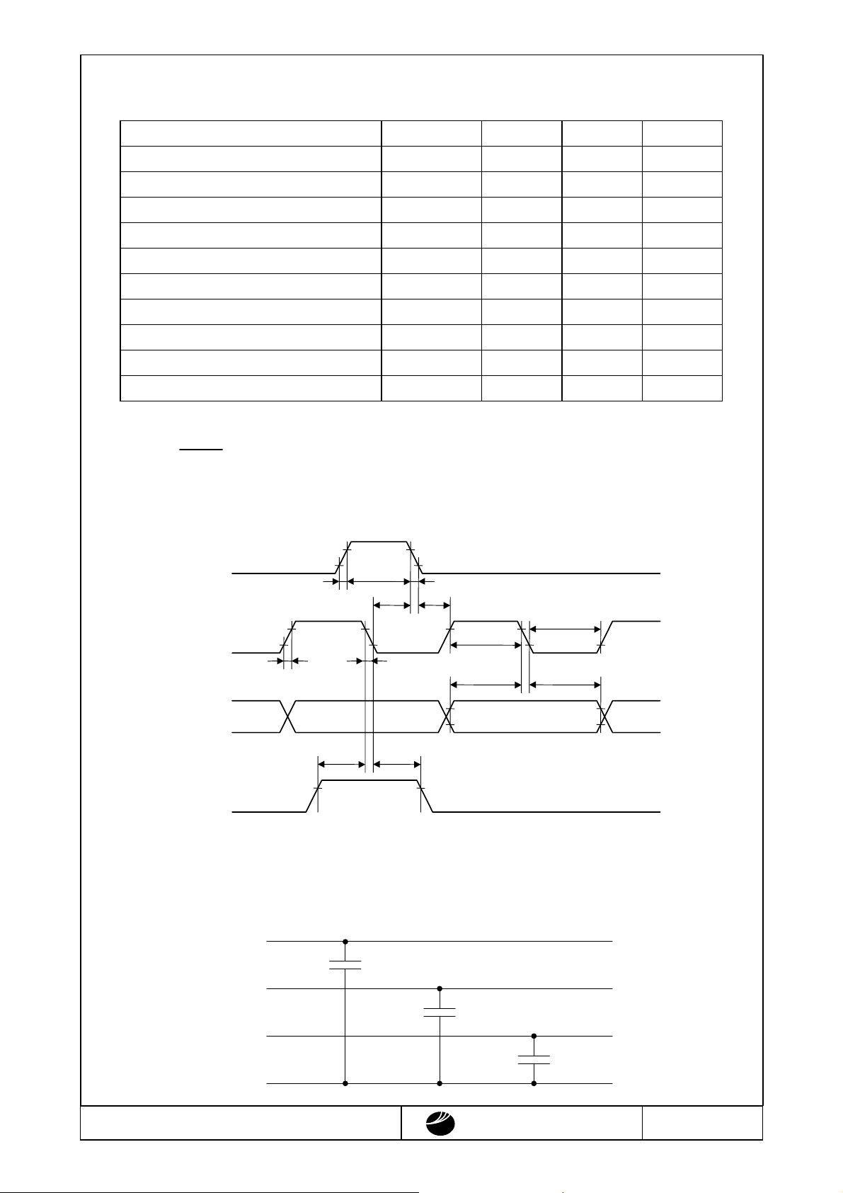
2.3.AC Characteristics
Parameter Symbol Min. Max. Units
=5.0V±10%
V
CC
CP Frequency
Clock Pulse Width
Load Pulse Width
Data Setup Time
Data Hold Time
Clock Pulse Setup Time
Clock Pulse Hold Time
Rise/Fall Time
FLM Setup Time
FLM Hold Time
f
CP
t
50 - ns
WC
t
63 - ns
WL
t
30 - ns
SETUP
t
30 - ns
HOLD
t
80 - ns
CL
t
0 - ns
LC
t
r, tf
t
100 - ns
FDS
t
100 - ns
FDH
6.0 MHz
-
Note 1 ns
-
Note 1:The rise and fall times (tr, tf ) must satisfy the following relationships (①and ②).
t
r, tf
①
t
r, tf< 50 ns
②
<
1
-
2fCP
t
WC
LOAD
t
t
r
WL
t
CL
t
f
t
LC
CP
t
WC
t
t
r
f
t
SETUP
D0~D3
t
FDS
t
FDH
FLM
This module contain these capacitors. Please be careful about timing characteristics.
FLM
1000pF
LP
M
VSS
470pF
t
WC
t
HOLD
1000pF
DMF-50174ZNB-FW (AT) No.2000-0166 OPTREX CORPORATION Page 4/18
OPTREX
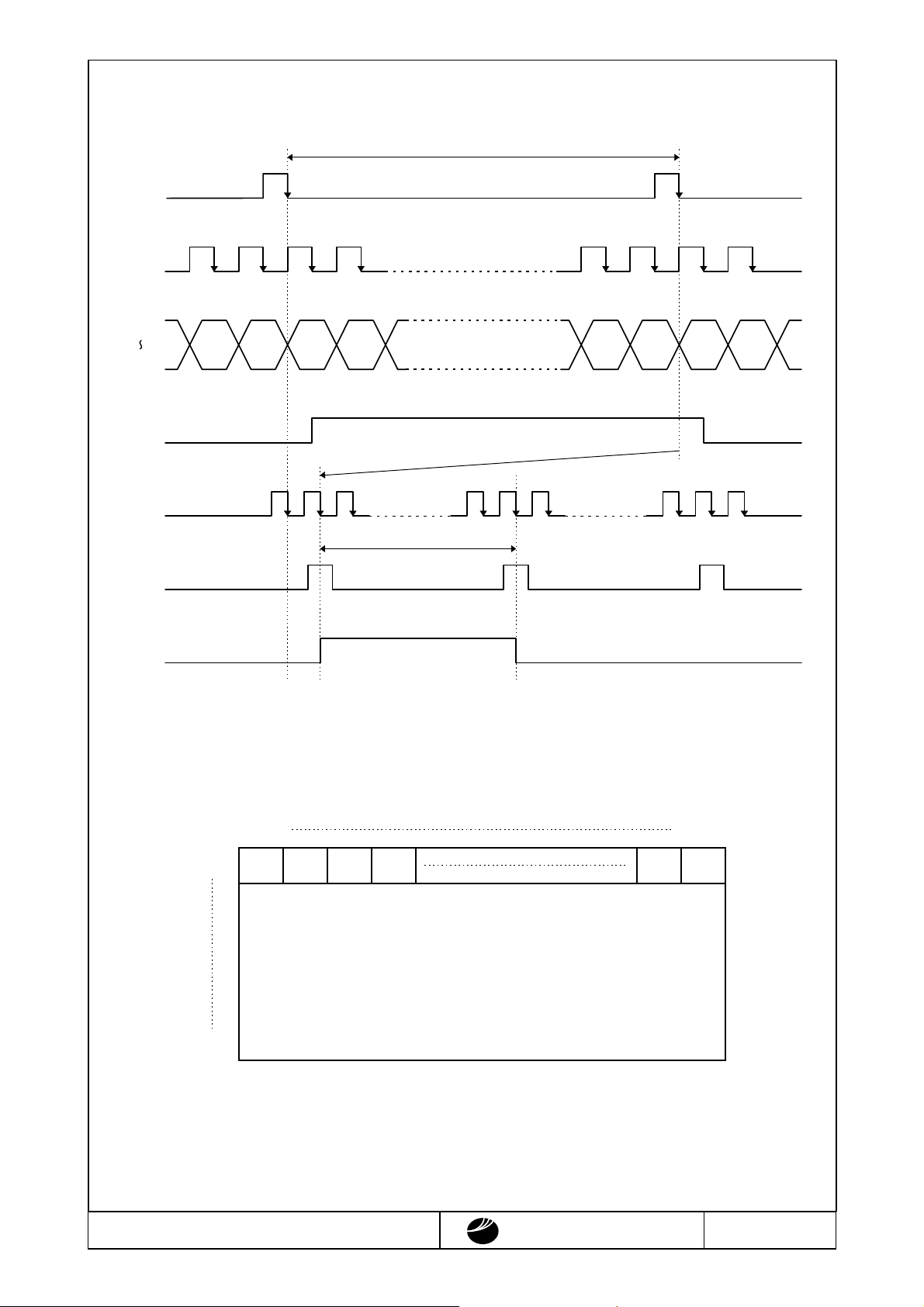
2.4.Timing Chart
LP
CP
D0
~
D3
FLM
LP
(Reduction)
FLM
(Reduction)
M
313
SEGSEG SEGSEG SEGSEG SEGSEG
~
~
317
320316 84320316 84
1
~
2.5.Comparison of Display and Data
SEG1 SEG320
#1
#240
D2D3
T=0.0595ms typ.
~
5
240×T
D0D1 D0D1
#1 DATA
TOP VIEW
D0~D3
313
317
~
~
1
5
~
~
DMF-50174ZNB-FW (AT) No.2000-0166 OPTREX CORPORATION Page 5/18
OPTREX
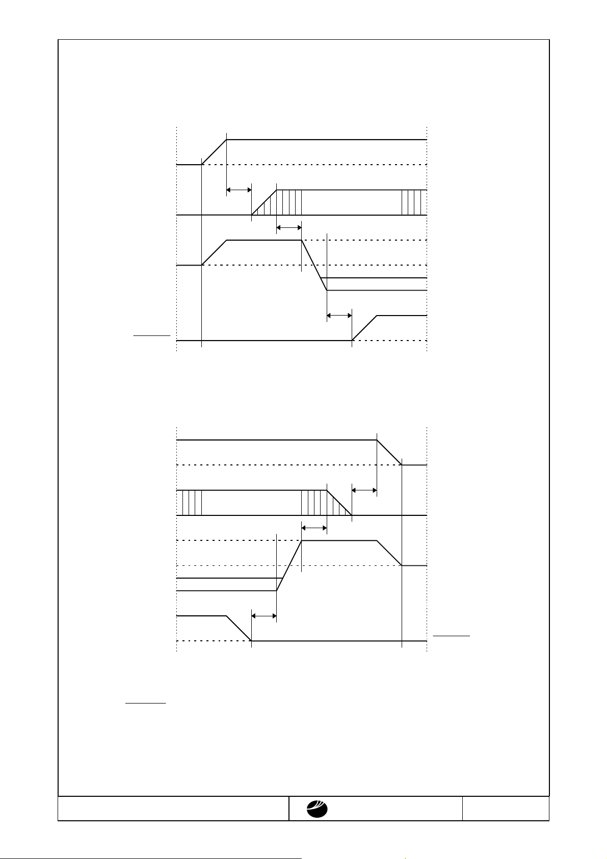
2.6.Power Supply ON/OFF Sequence
2.6.1.ON Sequence
SIGNAL
LEVEL
VCC
VCC
0≦t
SIGNAL
0≦t
VSS
VCC
VSS
VCC
VADJ
VEE
DISPOFF
0≦t
VSS
VADJ
VEE
VCC
VSS
2.6.2.OFF Sequence
LEVEL
VCC
SIGNAL
VSS
VCC
VSS
VCC
0≦t
VCC
0≦t
SIGNAL
VSS
VADJ
VEE
VCC
VSS
0≦t
VADJ
VEE
DISPOFF
Please maintain the above sequence when turning on and off the power supply of the module.
If DISPOFF is supplied to the module
hile internal alternate signal for LCD driving (M) is
w
unstable, DC component will be supplied to the LCD panel. This may cause damage the LCD
module.
DMF-50174ZNB-FW (AT) No.2000-0166 OPTREX CORPORATION Page 6/18
OPTREX
 Loading...