

OPTREX DMF50036NB-FW, DMC5003NB-FW Datasheet
DMF5003NB-FW (AA) No.97-0063 OPTREX CORPORATION Page 1/16
OPTREX
Type No.
*******
March 24, 1997
First Edition
Final Revision
Quality Assurance Div.
Production Div.
Checked by
Checked by
Approved by
Production Div.
Design Engineering Div.
Prepared by
LCD Module Specification
DMF5003NB-FW
DMF5003NB-FWDMF5003NB-FW
DMF5003NB-FW
Table of Contents
1. General Specifications .............................................................................2
2. Electrical Specifications...........................................................................3
3. Optical Specifications..............................................................................7
4. I/O Terminal.............................................................................................9
5. Test..........................................................................................................11
6. Appearance Standards............................................................................12
7. Code System of Production Lot ..........................................................15
8. Type Number..........................................................................................15
9. Applying Precautions .............................................................................15
10. Handling Precautions.............................................................................16
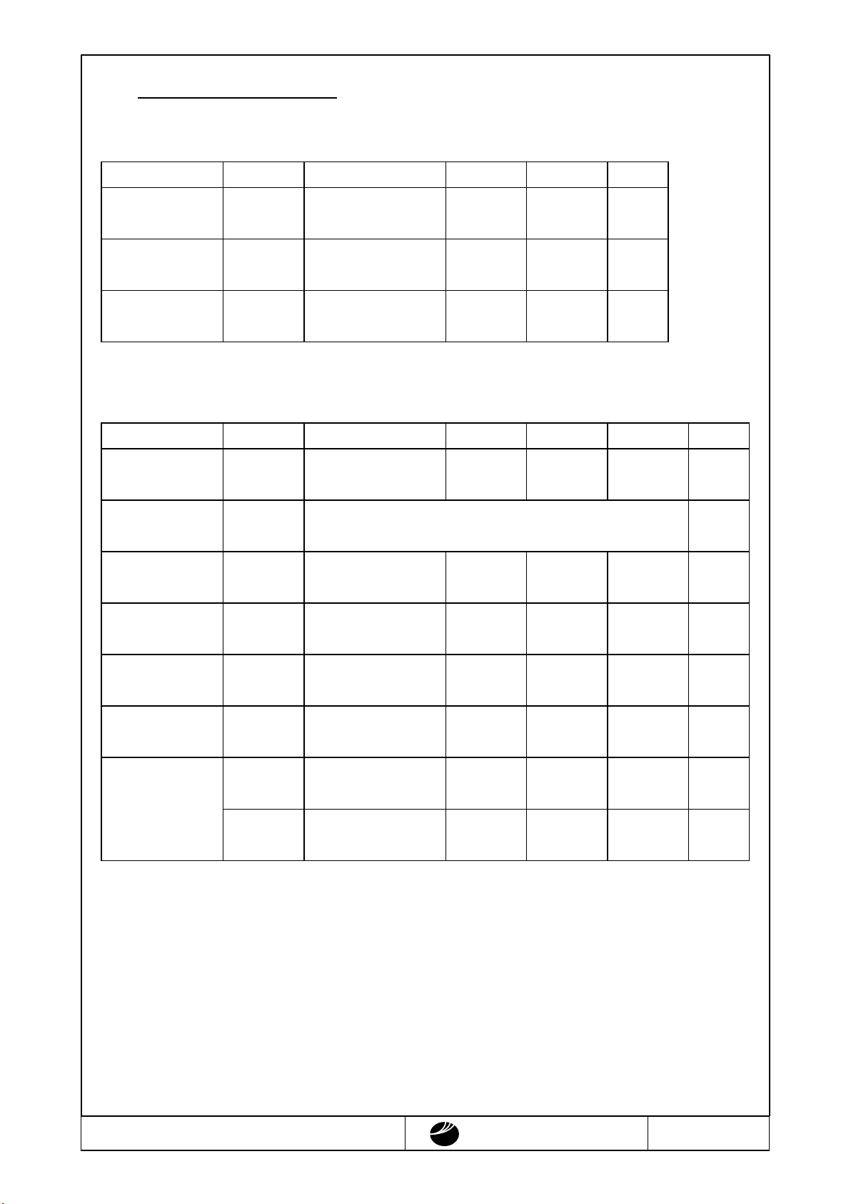
Revision History
Rev. Date Page Comment
DMF5003NB-FW (AA) No.97-0063 OPTREX CORPORATION Page 2/16
OPTREX
1.General Specifications
Operating Temp.
:
min. 0℃ ~ max. 50℃
Storage Temp.
:
min. -20℃ ~ max. 60℃
Dot Pixels
:
160 (W) × 128 (H) dots
Dot Size
:
0.54 (W) × 0.54 (H) mm
Dot Pitch
:
0.58 (W) × 0.58 (H) mm
Viewing Area
:
101.0 (W) × 82.0 (H) mm
Outline Dimensions
:
152.0
*
(W) × 112.0 (H) × 23.0 max.** (D) mm
*
Without CFL Cable
** Without Connector
W eight
:
260g max.
LCD Type
:
NTD-7353
( STN / Blue-mode / Transmissive )
Viewing Angle
:
6:00
Control LSI
:
T6963C-0101 (Produced by TOSHIBA)
Data Transfer
:
8-bit parallel data transfer
Backlight
:
Cold Cathode Fluorescent Lamp (CFL) × 1
Drawings
:
Dimensional Outline UE-34607A
DMF5003NB-FW (AA) No.97-0063 OPTREX CORPORATION Page 3/16
OPTREX
2.Electrical Specifications
2.1.Absolute Maximum Ratings
V
SS
=0V
Parameter Symbol Conditions Min. Max. Units
Supply Voltage
(Logic)
VCC-VSS
-
-0.3 7.0 V
Supply Voltage
(LCD Drive)
VCC-V
ADJ
-
0 28.0 V
Input Voltage VI
-
-0.3 VCC+0.3 V
2.2.DC Characteristics
Ta=25℃, V
SS
=0V
Parameter Symbol Conditions Min. Typ. Max. Units
Supply Voltage
(Logic)
VCC-VSS
-
4.5 - 5.5 V
Supply Voltage
(LCD Drive)
VCC-V
ADJ
Shown in 3.1 V
High Level
Input Voltage
VIH VCC=5.0V±10% VCC-2.2
-
V
CC
V
Low Level
Input Voltage
VIL VCC=5.0V±10% 0 - 0.8 V
High Level
Output Voltage
VOH IOH=-0.75mA VCC-0.3
-
V
CC
V
Low Level
Output Voltage
VOL IOL=0.75mA 0 - 0.3 V
Supply Current
ICC VCC-VSS=5.0V
-
9.3 20.0 mA
I
EE
VCC-V
ADJ
=18.5V
-
3.9 10.0 mA
DMF5003NB-FW (AA) No.97-0063 OPTREX CORPORATION Page 4/16
OPTREX
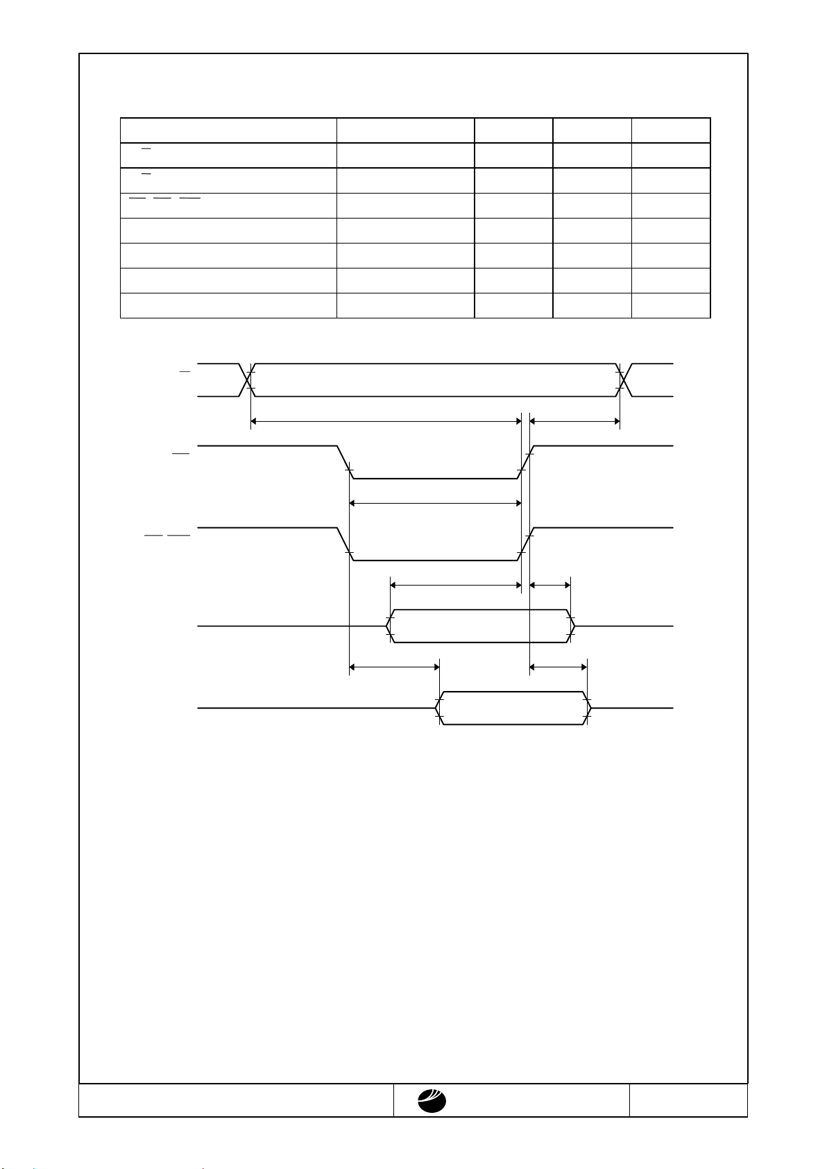
2.3.AC Characteristics
V
CC
=5.0V±10%
Parameter Symbol Min. Max. Units
C/D Setup Time
t
CDS
100 - ns
C/D Hold Time
t
CDH
10 - ns
CE, RD, WR Pulse Width
t
CE
,
t
RD
,
t
WR
80 - ns
Data Setup Time
t
DS
80 - ns
Data Hold Time
t
DH
40 - ns
Access Time
t
ACC
-
150 ns
Output Hold Time
t
OH
10 50 ns
(WRITE)
(READ)
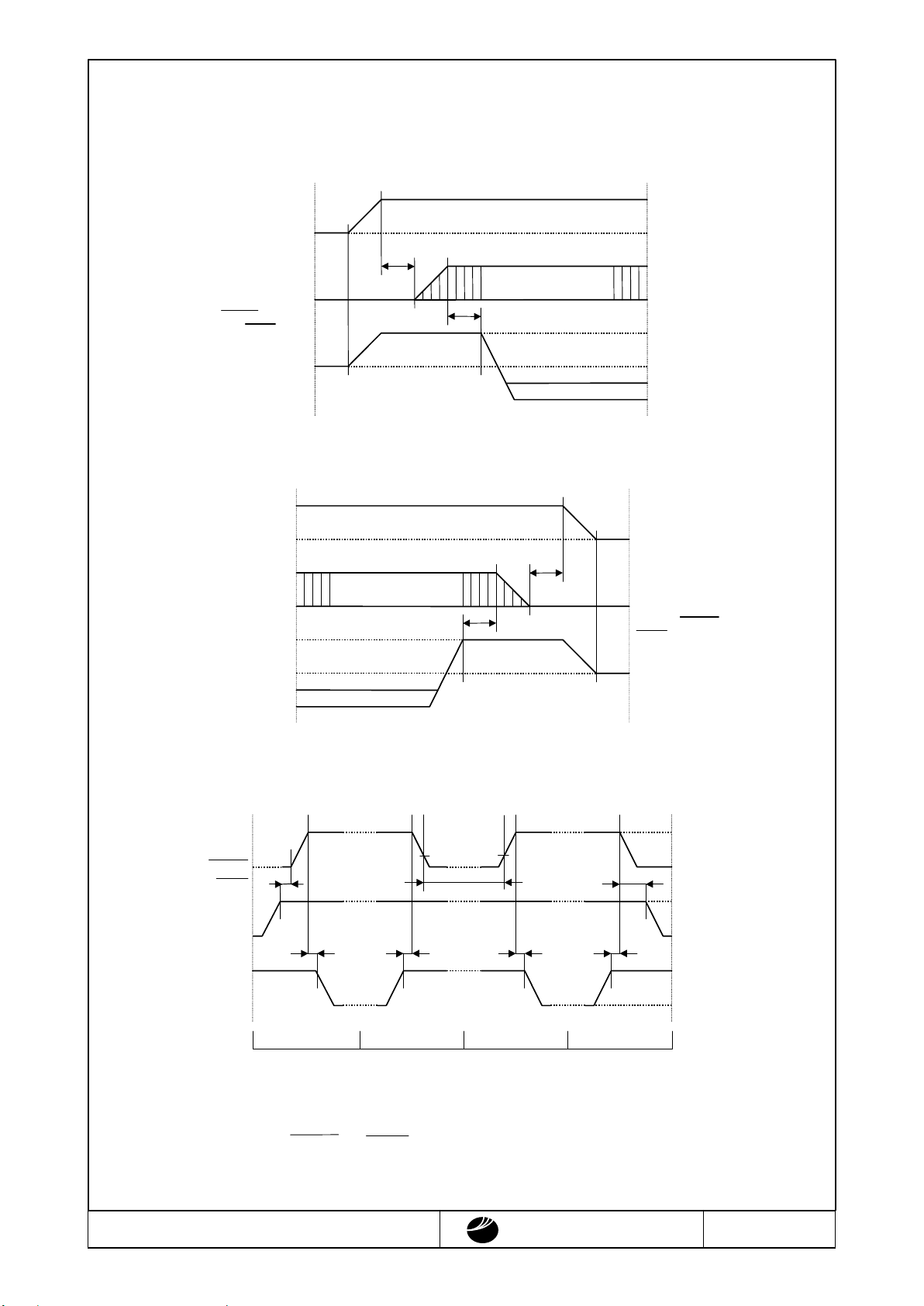
RD, WR
D0~D7
CE
C/D
D0~D7
t
DS
t
OH
t
DH
t
ACC
t
CE, tRD, tWR
t
CDH
t
CDS
DMF5003NB-FW (AA) No.97-0063 OPTREX CORPORATION Page 5/16
OPTREX
2.4.Power Supply ON/OFF Sequence
2.4.1.ON Sequence
2.4.2.OFF Sequence
2.4.3.Reset Sequence
Please maintain the above sequence when turning on and off the power supply of the module.
If V
EE
and/or V
CONT
is supplied to the module while internal alternate signal for LCD driving
(M) is unstable or RESET and HALT is active, DC component will be supplied to the LCD
panel. This may cause damage to the LCD module.
RESET
VDD
VCONT
SIGNAL
T≧0
T≧0T≧0T≧50msT≧50ms
T>250μs
LEVEL
L Level
H Level
VDD
VCONT
VDD
VSS
Power OffPower On Reset CancellationReset
T≧10 ms
HALT
VEE
VSS
VSS
VDD
VSS
VDD
VDD
VEE
0≦t
SIGNAL
0≦t
SIGNAL
VDD
LEVEL
VCONT
VCONT
(Without RESET and
HALT Signal)
VEE
VSS
VSS
VDD
VSS
VDD
VDD
VEE
0≦t
SIGNAL
0≦t
SIGNAL
VDD
LEVEL
VCONT
VCONT
(Without RE S E T and
HALT Signal)
 Loading...