

OPTREX DMC40131, DMC32131 Datasheet
DMC40131* (BA) No.98-0165 OPTREX CORPORATION Page 1/15
OPTREX
Type No.
*******
July 3, 1998
First Edition
Final Revision
Quality Assurance Div.
Production Div.
Checked by
Checked by
Approved by
Production Div.
Design Engineering Div.
Prepared by
LCD Module Specification
DMC40131*
DMC40131*DMC40131*
DMC40131*
Table of Contents
1. General Specifications.............................................................................2
2. Electrical Specifications...........................................................................3
3. Optical Specifications..............................................................................6
4. I/O Terminal.............................................................................................8
5. Test..........................................................................................................10
6. Appearance Standards............................................................................11
7. Code System of Production Lot..........................................................14
8. Applying Precautions.............................................................................14
9. Handling Precautions.............................................................................15
Revision History
Rev. Date Page Comment
DMC40131* (BA) No.98-0165 OPTREX CORPORATION Page 2/15
OPTREX
1.General Specifications
Operating Temp.
:
min. 0℃ ~ max. 50℃
Storage Temp.
:
min. -20℃ ~ max. 60℃
Display Format
:
40 characters × 1 lines
Display Fonts
:
5 × 11 dots ( 1 character )
Viewing Area
:
152.5 (W) × 16.5 (H) mm
Outline Dimensions
:
182.0 (W) × 33.5 (H) × (11.0) (D) mm
W eight
:
75 g max.
LCD Type
:
FRD-7134
( TN / Clear -mode / Reflective )
Viewing Angle
:
6:00
Backlight
:
None
Drawings
:
Dimensional Outline UE-34066B
DMC40131* (BA) No.98-0165 OPTREX CORPORATION Page 3/15
OPTREX
2.Electrical Specifications
2.1.Absolute Maximum Ratings
V
SS
=0V
Parameter Symbol Conditions Min. Max. Units
Supply Voltage
(Logic)
VCC-VSS
-
-0.3 7.0 V
Supply Voltage
(LCD Drive)
VCC-VEE
-
0 13.0 V
Input Voltage VI
-
-0.3 VCC+0.3 V
2.2.DC Characteristics
Ta=25℃, V
SS
=0V
Parameter Symbol Conditions Min. Typ. Max. Units
Supply Voltage
(Logic)
VCC-VSS
-
4.5 - 5.5 V
Supply Voltage
(LCD Drive)
VCC-VEE Shown in 3.1 V
High Level
Input Voltage
VIH VCC=5.0V±10% 2.2 - V
CC
V
Low Level
Input Voltage
VIL VCC=5.0V±10% 0 - 0.6 V
High Level
Output Voltage
VOH IOH=-0.205mA 2.4 - V
CC
V
Low Level
Output Voltage
VOL IOL=1.2mA 0 - 0.4 V
Supply Current
ICC VCC-VSS=5.0V
-
2.0 3.0 mA
I
EE
VCC-VEE=3.7V
-
0.5 0.8 mA
DMC40131* (BA) No.98-0165 OPTREX CORPORATION Page 4/15
OPTREX
2.3.AC Characteristics
V
CC
=5.0V±10%
Parameter Symbol Conditions Min. Max. Units
Enable Cycle Time
t
CYC
Fig.1, 2 500
-
ns
Enable Pulse Width PWEH Fig.1, 2 230
-
ns
Enable Rise/Fall Time
t
E
r,
t
E
f Fig.1, 2 - 20 ns
Address Setup Time
t
AS
Fig.1, 2 40
-
ns
Address Hold Time
t
AH
Fig.1, 2 10
-
ns
Write Data Setup Time
t
DSW
Fig.1 80 - ns
Write Data Hold Time
t
DHW
Fig.1 10 - ns
Read Data Delay Time
t
DDR
Fig.2 - 160 ns
Read Data Hold Time
t
DHR
Fig.2 5
-
ns
Fig.1 Write Operation Timing
Fig.2 Read Operation Timing
E
R/W
V
IH
V
IL
PW
EH
V
IL
t
CYC
t
E
r
t
E
f
t
DSW
t
DHW
t
AH
t
AS
V
IL
RS
DB0~DB7
Valid Data
V
IH
V
IL
V
IH
V
IL
V
IH
V
IL
V
IL
V
IH
V
IL
V
IH
V
IL
E
R/W
V
IH
V
IH
V
IH
PW
EH
t
DDR
t
E
f
t
CYC
t
DHR
t
E
r
t
AH
t
AS
V
IL
RS
DB0~DB7
Valid Data
V
IH
V
IL
V
IH
V
IL
V
IH
V
IL
V
IL
V
OH
V
OL
V
OH
V
OL
DMC40131* (BA) No.98-0165 OPTREX CORPORATION Page 5/15
OPTREX
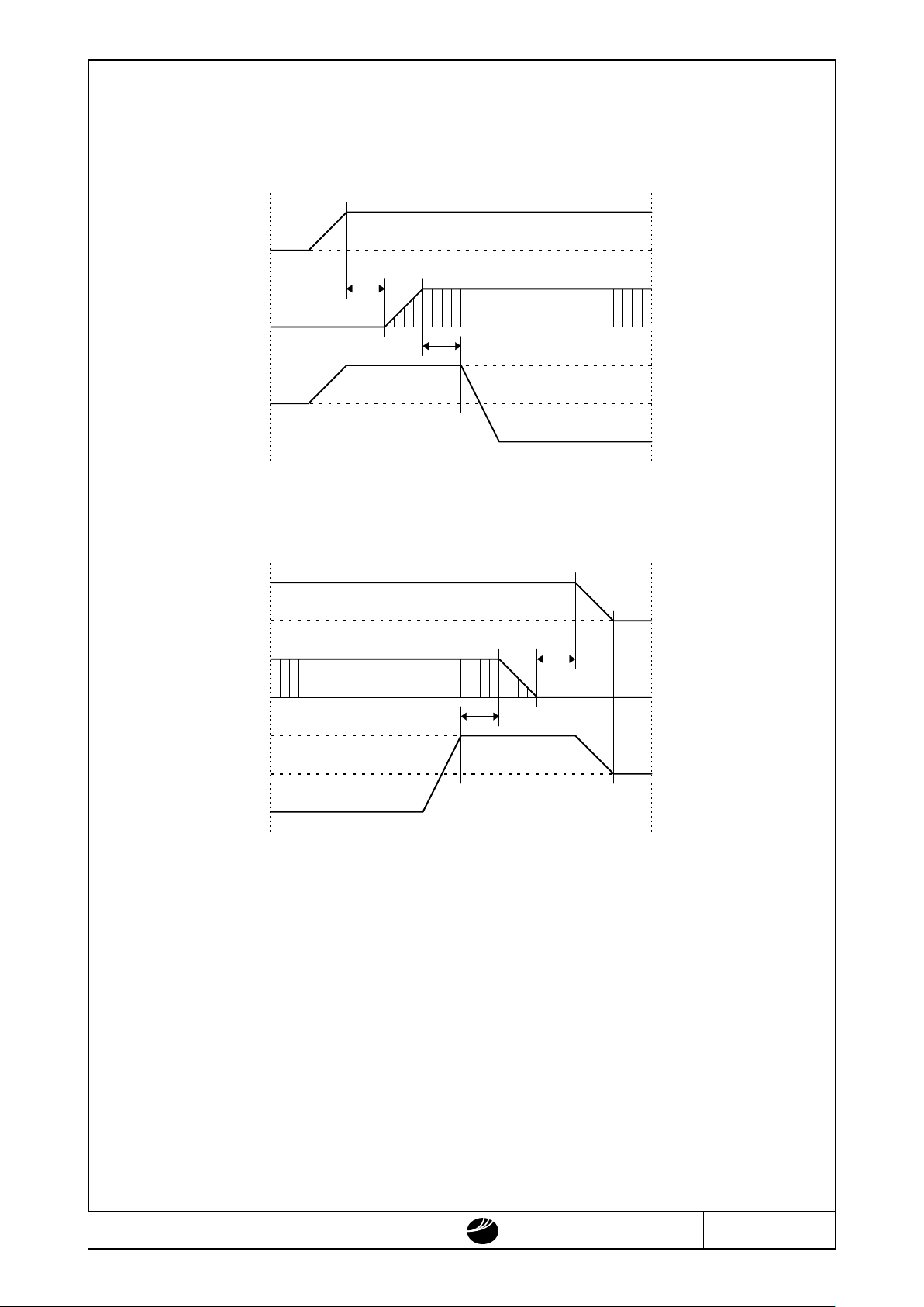
2.4.Power Supply ON/OFF Sequence
2.4.1.ON Sequence
2.4.2.OFF Sequence
Please maintain the above sequence when turning on and off the power supply of the module.
If V
EE
is supplied to the module while internal alternate signal for LCD driving (M) is unstable,
DC component will be supplied to the LCD panel. This may cause damage the LCD module.
VEE
VSS
VSS
VCC
VSS
VCC
VEE
VCC
0≦t
0≦t
SIGNAL
SIGNAL
LEVEL
VCC
VEE
VSS
VSS
VCC
VSS
VCC
VEE
VCC
0≦t
0≦t
SIGNAL
SIGNAL
LEVEL
VCC
 Loading...