

OPTREX DMC32132 Datasheet
LCD Module Specification
First Edition
Jun 29, 1999
Final Revision
*******
Approved by
Checked by
Checked by
Production Div.
Quality Assurance Div.
Design Engineering Div.
Type No.
DMC32132
DMC32132
DMC32132DMC32132
Table of Contents
Prepared by
1. General Specifications .............................................................................2
2. Electrical Specifications...........................................................................3
3. Optical Specifications..............................................................................5
4. I/O Terminal.............................................................................................7
5. Test............................................................................................................9
6. Appearance Standards............................................................................10
7. Code System of Production Lot ..........................................................13
8. Type Number..........................................................................................13
9. Applying Precautions .............................................................................13
10. Precautions Relating Product Handling................................................14
11. Warranty..................................................................................................15
Revision History
Rev. Date Page Comment
Production Div.
DMC32132 (AA) No.99-0183 OPTREX CORPORATION Page 1/15
OPTREX
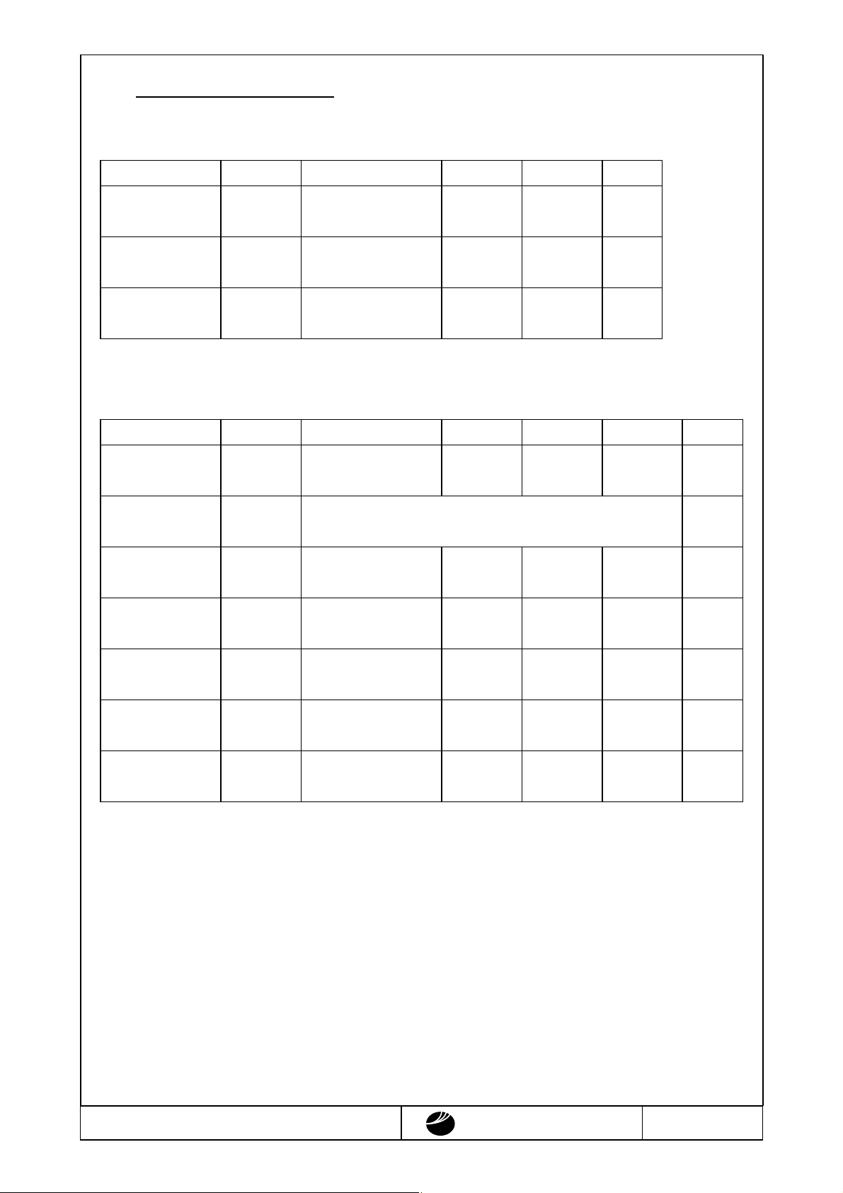
1.General Specifications
Operating Temp.
Storage Temp.
Display Format
Display Fonts
Viewing Area
Outline Dimensions
W eight
LCD Type
Viewing Angle
Backlight
Drawings
min. 0℃ ~ max. 50℃
:
min. -20℃ ~ max. 70℃
:
32 characters × 1 line
:
5 × 11 dots
:
123.5 (W) × 24.0 (H) mm
:
174.5 (W) × 31.0 (H) × 11.0 max. (D) mm
:
60 g max.
:
FRD-7135
:
( TN / Clear / Reflective )
6:00
:
None
:
Dimensional Outline UE-20055
:
DMC32132 (AA) No.99-0183 OPTREX CORPORATION Page 2/15
OPTREX
2.Electrical Specifications
2.1.Absolute Maximum Ratings
Parameter Symbol Conditions Min. Max. Units
=0V
V
SS
Supply Voltage
(Logic)
Supply Voltage
(LCD Drive)
Input Voltage VI
2.2.DC Characteristics
Parameter Symbol Conditions Min. Typ. Max. Units
Supply Voltage
(Logic)
Supply Voltage
(LCD Drive)
High Level
Input Voltage
VDD-VSS
VDD-VEE
VDD-VSS
-0.3 7.0 V
-
0 13.0 V
-
-0.3 VDD+0.3 V
-
Ta=25℃, V
4.5 - 5.5 V
-
SS
=0V
VDD-VEE Shown in 3.1 V
VIH VDD=5.0V±10% 2.2 - V
V
DD
Low Level
VIL VDD=5.0V±10% 0 - 0.6 V
Input Voltage
High Level
VOH IOH=-0.205mA 2.4 - V
Output Voltage
Low Level
VOL IOL=1.2mA 0 - 0.4 V
Output Voltage
Supply Current IDD VDD-VSS=5.0V
V
DD
2.0 5.0 mA
-
DMC32132 (AA) No.99-0183 OPTREX CORPORATION Page 3/15
OPTREX
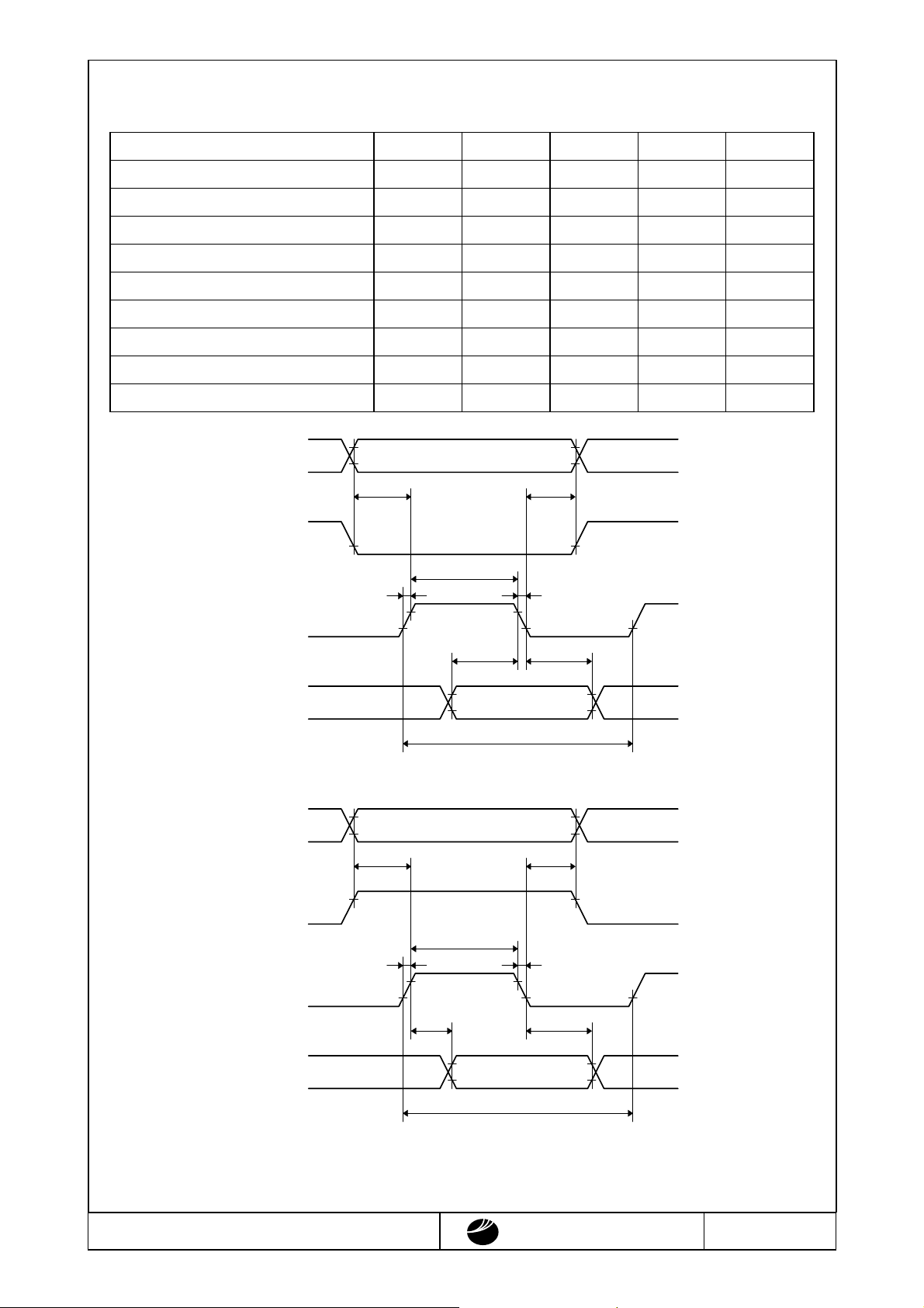
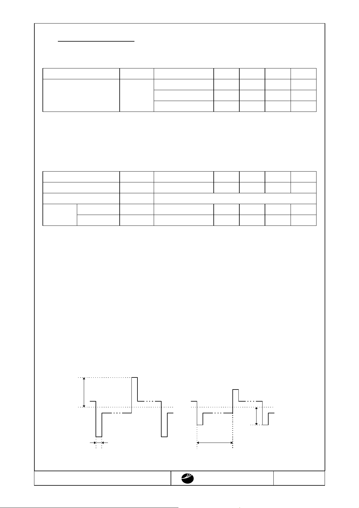
2.3.AC Characteristics
Parameter Symbol Conditions Min. Max. Units
=5.0V±10%
V
DD
Enable Cycle Time
t
Fig.1, 2 500
CYC
Enable Pulse Width PWEH Fig.1, 2 230
t
Enable Rise/Fall Time
Address Setup Time
Address Hold Time
Write Data Setup Time
Write Data Hold Time
Read Data Delay Time
Read Data Hold Time
t
r,
f Fig.1, 2 - 20 ns
E
E
t
Fig.1, 2 40
AS
t
Fig.1, 2 10
AH
t
Fig.1 80 - ns
DSW
t
Fig.1 10 - ns
DHW
t
Fig.2 - 160 ns
DDR
t
Fig.2 5
DHR
RS
V
IH
V
IL
t
AS
V
IH
V
IL
t
AH
R/W
DB0~DB7
t
CYC
V
IL
f
E
t
V
IL
t
DHW
V
V
V
IL
PW
EH
r
E
t
V
E
V
IH
IL
V
V
IH
IL
t
DSW
V
IH
Valid Data
Fig.1 Write Operation Timing
RS
V
IH
V
IL
t
AS
V
IH
V
IL
t
AH
V
R/W
IH
V
IH
PW
r
E
E
t
V
V
IL
EH
f
E
t
IH
V
IH
V
IL
t
DB0~DB7
DDR
V
V
OH
OL
Valid Data
t
CYC
t
DHR
V
OH
V
OL
Fig.2 Read Operation Timing
ns
-
ns
-
ns
-
ns
-
ns
-
V
IL
IH
IL
V
IL
DMC32132 (AA) No.99-0183 OPTREX CORPORATION Page 4/15
OPTREX
3.Optical Specifications
(
)
(
)
3.1.LCD Driving Voltage
Parameter Symbol Conditions Min. Typ. Max. Units
Recommended Ta= 0℃
-
4.4 V
-
LCD Driving Voltage VDD-VEE Ta=25℃ 3.4 3.7 4.0 V
Note 1 Ta=50℃ 3.1 -
Note 1 : Voltage (Applied actual waveform to LCD Module) for the best contrast. The range of
minimum and maximum shows tolerance of the operating voltage. The specified contrast ratio and
response time are not guaranteed over the entire range.
3.2.Optical Characteristics
Ta=25℃, 1/11 Duty, 1/4 Bias, V
=3.7V (Note 4), θ=10゚, φ=270゚
D
Parameter Symbol Conditions Min. Typ. Max. Units
Contrast Ratio Note 1 CR
=20゚, φ=270゚
θ
8 -
-
Viewing Angle Shown in 3.3
Response Rise Note 2 TON
Time Decay Note 3 T
OFF
-
-
240 360 ms
-
80 160 ms
-
Note 1 : Contrast ratio is definded as follows.
CR = L
L
: Luminance of the ON segments
ON
L
: Luminance of the OFF segments
OFF
OFF
/ LON
Note 2 : The time that the luminance level reaches 90% of the saturation level from 0% when ON
signal is applied.
Note 3 : The time that the luminance level reaches 10% of the saturation level from 100% when OFF
signal is applied.
Note 4 : Definition of Driving Voltage V
D
Assuming that the typical driving waveforms shown below are applied to the LCD Panel at
1/A Duty - 1/B Bias ( A : Duty Number, B : Bias Number ). Driving voltage V
as follows.
V
= (Vth1+Vth2) / 2
D
Vth1 : The volt age V
that should provide 50% of the satulation level in the luminance
O-P
measured atθ= 10゚, φ=270゚on the segment which the ON signal is applied to.
Vth2 : The volt age V
that should provide 26% of the satulation level in the luminance
O-P
measured atθ= 40゚, φ=270゚on the segment which the OFF signal is applied to.
O-P
V
×
f
A
F
1 /
1 /
f
F
B-2
〈
ON SIGNAL
〉
〈
OFF SIGNAL
〉
-
is definded
D
×
V
/ B
O-P
V
DMC32132 (AA) No.99-0183 OPTREX CORPORATION Page 5/15
OPTREX
 Loading...