

OPTREX C-51505NFQJ-LW-AD Datasheet
C-51505NFQJ-LW-AD (AD) No. 2002-0179 OPTREX CORPORATION Page 1/18
LCD Module Technical Specification
C-51505NFQJ-LW-AD
Table of Contents
1. General Specifications..................................................................................................................................2
2. Electrical Specifications...............................................................................................................................3
3. Optical Specifications ...................................................................................................................................7
4. I/O Terminal ...................................................................................................................................................... 9
5. Test ................................................................................................................................................................... 11
6. Appearance Standards................................................................................................................................12
7. Code System of Production Lot ............................................................................................................... 16
8. Type Number..................................................................................................................................................16
9. Applying Precautions ..................................................................................................................................16
10. Precautions Relating Product Handling................................................................................................17
11. Warranty........................................................................................................................................................18
Checked by (Design Engineering Div.)
Checked by (Quality Assurance Div.)
Approved by (Production Div.)
Prepared by (Production Div.)
Revision History
Rev. Date Page Comment
Type No.
Jun 28, 2002
OPTREX
First Edition
Final Revision
******
C-51505NFQJ-LW-AD (AD) No. 2002-0179 OPTREX CORPORATION Page 2/18
1. General Specifications
Operating Temp. : min. -20°C ~ max. 70°C
Storage Temp. : min. -20°C ~ max. 70°C
Display Format : 20 characters × 2 lines
Display Fonts : 5 × 8 dots ( 1 character )
Viewing Area : 83.0 (W) × 18.6 (H) mm
Outline Dimensions : 116.0 (W) × 37.0 (H) × (15.6) (D) mm
Weight : 42.9g max.
LCD Type : NTD-21333
( STN / Color-mode / Transmissive)
Viewing Angle : 6:00
Data Transfer : 8-bit parallel data transfer
Backlight : LED Backlight / White
Additional Spec : Vivid Color Display Specification
(High Performance Color Film is Used)
Drawings : Dimensional Outline UE-311044
C-51505NFQJ-LW-AD (AD) No. 2002-0179 OPTREX CORPORATION Page 3/18
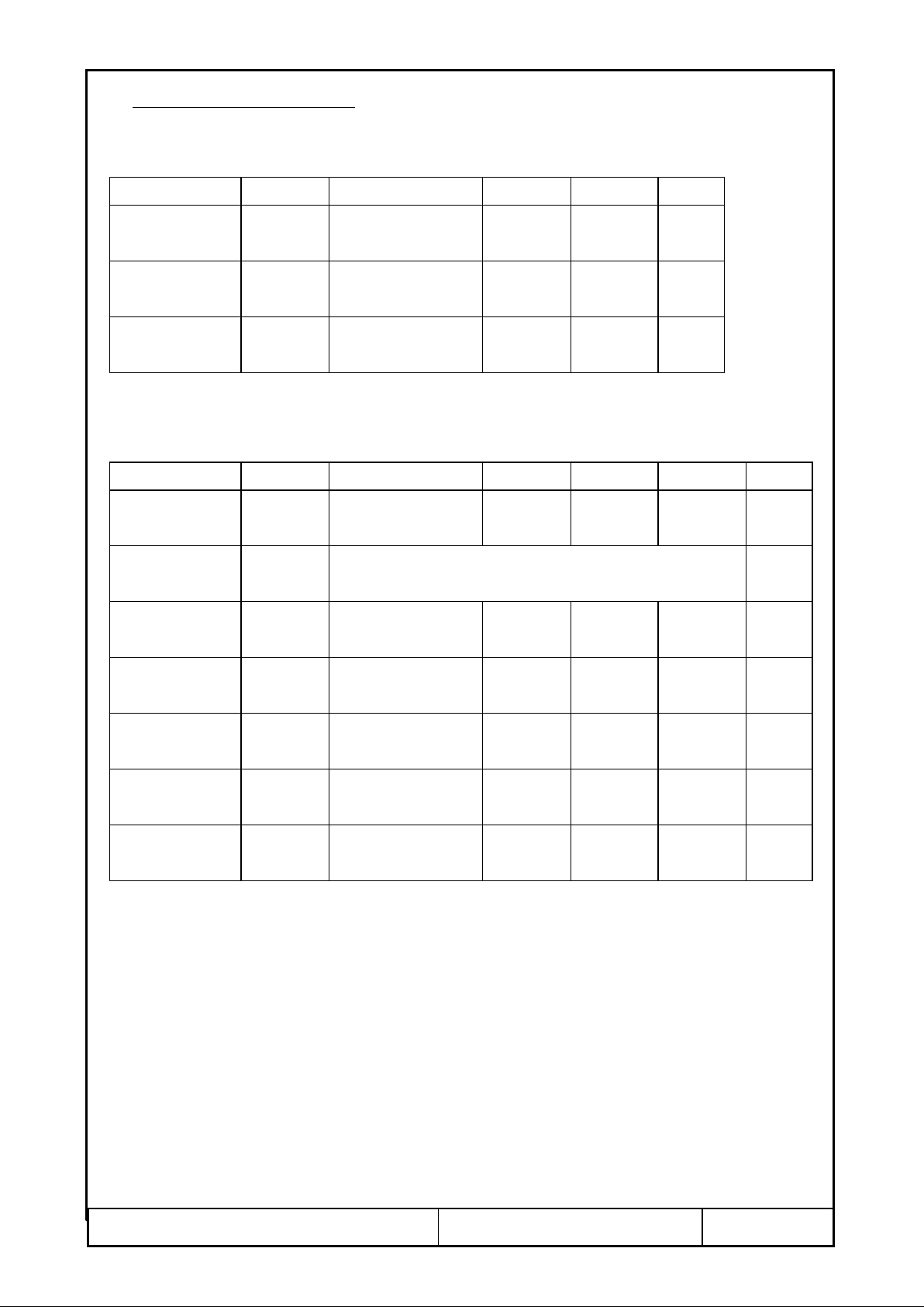
2. Electrical Specifications
2.1. Absolute Maximum Ratings
VSS=0V
Parameter Symbol Conditions Min. Max. Units
Supply Voltage
(Logic)
VCC-VSS - -0.3 7.0 V
Supply Voltage
(LCD Drive)
VCC-VEE - -0.3 13.5 V
Input Voltage VI - -0.3 VCC+0.3 V
2.2. DC Characteristics
Ta=25°C, VCC=5V, VSS=VEE=0V
Parameter Symbol Conditions Min. Typ. Max. Units
Supply Voltage
(Logic)
VCC-VSS - 4.5 - 5.5 V
Supply Voltage
(LCD Drive)
VCC-VEE Shown in 3.1 V
High Level
Input Voltage
VIH - 2.2 - VCC V
Low Level
Input Voltage
VIL - -0.3 - 0.8 V
High Level
Output Voltage
VOH IOH=-0.25mA 2.4 - - V
Low Level
Output Voltage
VOL IOL=1.2mA - - 0.4 V
Supply Current ICC VCC-VSS=5.3V - 2.0 3.0 mA
All voltage values are referenced to VSS =0V
V1 to V5 must maintain VDD ≥ V1 ≥ V2 ≥ V3 ≥ V4 ≥V5.

C-51505NFQJ-LW-AD (AD) No. 2002-0179 OPTREX CORPORATION Page 4/18
2.3. AC Characteristic
Read Operation
VCC=5.0V±10%
Parameter Symbol Min. Max. Units
Enable Cycle Time
t
CYCE 500 - ns
Enable “H” Level Pulse Width
t
wHE 300 - ns
Enable Rise/Fall Time
t
RE, tFE - 25 ns
RS,R/W Setup Time (8-bit operation mode)
(4-bit operation mode)
t
AS
60
100
- ns
RS,R/W Address Hold Time
t
AH 10 - ns
Read Data Output Delay
t
RD - 190 ns
Read Data Hold Time
t
DHR 20 - ns
Read Operation Timing
E
R/W
V
IH
VIL
tWHE
VIL
tCYCE
tRE tFE
tRD tDHR
tAHtAS
V
IL
RS
DB0~DB7
Valid Data
V
IH
V
IL
V
IH
VIL
V
IH
VILVIL
V
IH
V
IL
V
IH
V
IL

C-51505NFQJ-LW-AD (AD) No. 2002-0179 OPTREX CORPORATION Page 5/18
Write Operation
VCC=5.0V±10%
Parameter Symbol Min. Max. Units
Enable Cycle Time
t
CYCE 500 - ns
Enable “H” Level Pulse Width
t
wHE 300 - ns
Enable Rise/Fall Time
t
RE, tFE - 25 ns
RS,R/W Setup Time (8-bit operation mode)
(4-bit operation mode)
t
AS
60
100
- ns
RS,R/W Address Hold Time
t
AH 10 - ns
Data Output Delay
t
DS - - ns
Data Hold Time
t
DHR 10 - ns
Write Operation Timing
E
R/W
VIHVIH
VIH
t
WHE
t
DS
t
FE
t
CYCE
t
DHW
t
RE
t
AH
t
AS
VIL
RS
DB0~DB7 Valid Data
VIH
VIL
VIH
V
IL
VIH
V
IL
V
IL
V
OH
VOL
V
OH
VOL
C-51505NFQJ-LW-AD (AD) No. 2002-0179 OPTREX CORPORATION Page 6/18
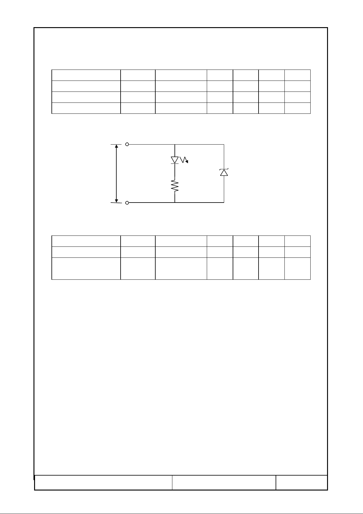
2.4. Lighting Specifications
2.4.1. Absolute Maximum Ratings
Ta=25°C
Parameter Symbol Conditions Min. Typ. Max. Units
Forward Voltage VF Note 1 - - 6.0 V
LED Power Dissipation PD - - - 0.125 mW
Reverse Voltage VR - - - 5.0 V
Note 1 : VF is defined as the voltage between ANODE and CATHODE as shown below.
2.4.2. Operating Characteristics
Ta=25°C
Parameter Symbol Conditions Min. Typ. Max. Units
Foward Current IF VF=5.0V - 15 18 mA
Luminance of
Backlight Surface
L VF=5.0V 125 - - cd/m
2
ANODE
CATHODE
R
VF
 Loading...