

OPTREX 3C92CTXV, 3C92CTX, 3C92CHR, 3C92C Datasheet
Prod uct Bul le tin 3C92C
August 1998
Op ti cally Cou pled Iso la tor
Type 3C92C, 3C92CHR, 3C92CTX, 3C92CTXV
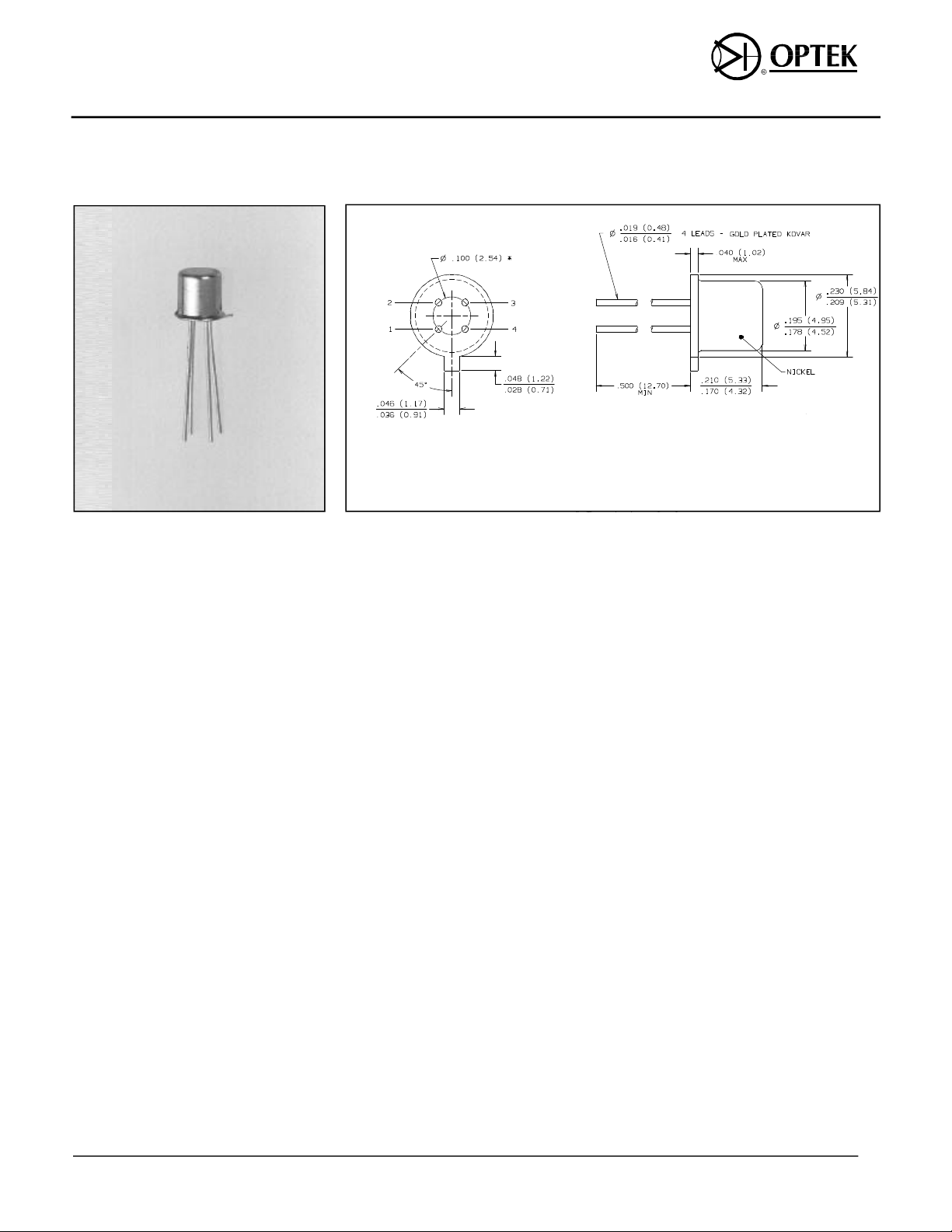
1 LED CATHODE
2 EMITTER
3 COLLECTOR
4 LED ANODE (Electrically connected to case)
*THIS DIMENSION IS CONTROLLED AT THE HOUSING SURFACE
DIMENSIONS ARE IN INCHES (MILLIMETERS)
Fea tures
• TO-72 hermetic package
• 1 kVDC electrical isolation
• High current transfer ratio
De scrip tion
The 3C92C is an optically coupled
isolator consisting of an infrared emitting
diode and an NPN silicon phototransistor
mounted in a hermetically sealed TO-72
package.
Typical screening and lot acceptance
tests are provided on page 13-4.
The 3C92CHR device has been 100%
screened as a TXV device although
Group B and C testing is not performed.
Ab so lute Maxi mum Rat ings (TA = 25o C un less oth er wise noted)
In put to Out put Iso la tion Volt age . . . . . . . . . . . . . . . . . . . . . . . . . . . . . . . . . ±1kVDC
Op er at ing Tem pera ture Range . . . . . . . . . . . . . . . . . . . . . . . . . . . . -55o C to +125o C
Stor age Tem pera ture Range . . . . . . . . . . . . . . . . . . . . . . . . . . . . . . -65o C to +150o C
Lead Sol der ing Tem pera ture [1/16 inch (1.6 mm) from case, 5 sec. with sol der ing
iron] . . . . . . . . . . . . . . . . . . . . . . . . . . . . . . . . . . . . . . . . . . . . . . . . . . . . . . . . 240o C
Power Dis si pa tion (Out put Tran sis tor). . . . . . . . . . . . . . . . . . . . . . . . . . . . . 200 mW
Power Dis si pa tion (In put Di ode). . . . . . . . . . . . . . . . . . . . . . . . . . . . . . . . . . . 60 mW
Notes:
(1) Measured with input leads shorted together and output leads shorted together.
(2) RMA flux is recommended. Duration can be extended to 10 sec. max. when flow soldering.
(3) Derate linearly 2.0 mW/o C above 25o C.
(4) Derate linearly 0.60 mW/o C above 65o C.
(1)
(2)
(3)
(4)
Op tek Tech nol ogy, Inc. 1215 W. Crosby Road Car roll ton, Texas 75006 (972)323- 2200 Fax (972)323- 2396
Types 3C92C, 3C92CHR, 3C92CTX, 3C92CTXV
Elec tri cal Char ac ter is tics (TA = 25o C un less oth er wise noted)
SYM BOL PA RAME TER MIN TYP MAX UNITS TEST CON DI TION
In put Di ode
V
V
I
R
C
Forward Voltage 1.2
F
Reverse Voltage 7 V IR = 0.1 mA
R
Reverse Current
Diode Capacitance 25 pF V = 0, f = 1 MHz
IN
Pho to tran sis tor
V
(BR)CEO
V
(BR)ECO
I
CEO
Collector-Emitter Breakdown Voltage 50 V IC = 10 mA
Emitter-Collector Breakdown Voltage
Collector-Emitter Leakage Current 10
Cou pled
I
C(ON)
V
CE(SAT)
t
t
C
R
on
off
On-State Collector Current 4.0
Collector-Emitter Saturation Voltage 0.4 V IF = 50 mA, IC = 10 mA
Turn on Time
Turn off Time
Input-to-Output Capacitance 2 2.5 pF f = 1 MHz
IO
Isolation Resistance
IO
1.5
1
7 V
50
—
3.0
20
9
6
9
10
VVIF = 2 mA
IF = 50 mA
VR = 3 V
µA
IC = 10 µA
nAnAVCE = 5 V
VCE = 50 V
mAmAIF = 10 mA, VCE = 5 V
IF = 10 mA, V
CE
= 0.4 V
µs VCC = 5 V, IC = 2 mA, RL = 100 Ω
µs
VIO = +1 kV
Ω
Op tek re serves the right to make changes at any time in or der to im prove de sign and to sup ply the best prod uct pos si ble.
Op tek Tech nol ogy, Inc. 1215 W. Crosby Road Car roll ton, Texas 75006 (972)323- 2200 Fax (972)323- 2396
 Loading...