

OPTREX 2N6989U Datasheet
Prod uct Bul le tin JANTX, JANTXV, 2N6989U
Janu ary 1996
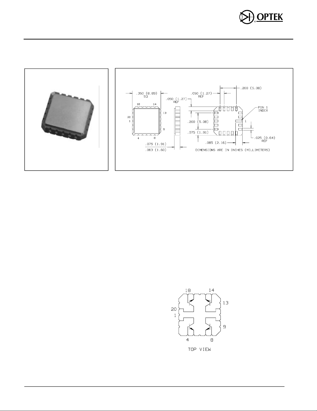
Sur face Mount Quad NPN Tran sis tor
Type JANTX, JANTXV, 2N6989U
Fea tures
• Ceramic surface mount package
• Hermetically sealed
• Small package minimizes circuit board
area required
• Electrical performance similar to a
2N2222A
• Qualification per MIL-PRF-19500/559
De scrip tion
The JANTX2N6989U is a hermetically
sealed, ceramic surface-mount device,
consisting of four individual silicon NPN
transistors. The 20 pin ceramic package
is ideal for designs where board space
and device weight are important design
considerations.
Typical screening and lot acceptance
tests are provided on page 13-4. The
burn-in condition is VCB = 30 V, PD = 250
mW each transistor, TA = 25o C. Refer
to MIL-PRF-19500/559 for complete
requirements.
When ordering parts without processing,
do not use a JAN prefix.
Ab so lute Maxi mum Rat ings (TA = 25o C un less oth er wise noted)
Collector- Base Volt age . . . . . . . . . . . . . . . . . . . . . . . . . . . . . . . . . . . . . . . . . . . . . 75 V
Collector- Emitter Volt age . . . . . . . . . . . . . . . . . . . . . . . . . . . . . . . . . . . . . . . . . . . 50 V
Emitter- Base Volt age . . . . . . . . . . . . . . . . . . . . . . . . . . . . . . . . . . . . . . . . . . . . . . 6.0 V
Col lec tor Current- Continuous. . . . . . . . . . . . . . . . . . . . . . . . . . . . . . . . . . . . . . 800 mA
Op er at ing Junc tion Tem pera ture(TJ) . . . . . . . . . . . . . . . . . . . . . . . . -65o C to +200o C
Stor age Junc tion Tem pera ture (T
Power Dis si pa tion (sin gle tran sis tor, no heat sink) . . . . . . . . . . . . . . . . . . . . . . . 0.5 W
Power Dis si pa tion TA = 25o C (four de vices driven equally). . . . . . . . . . . . . . . 1.0 W
Iso la tion Volt age . . . . . . . . . . . . . . . . . . . . . . . . . . . . . . . . . . . . . . . . . . . . . . . 500 Vdc
Notes:
(1) Derate linearly 8.57 mW/oC above 25o C.
) . . . . . . . . . . . . . . . . . . . . . . . . -65o C to +200o C
stg
(1)
Optek Technology, Inc. 1215 W. Crosby Road Carrollton, Texas 75006 (972)323-2200 Fax (972)323-2396
15-20
Type JANTX, JANTXV, 2N6989U
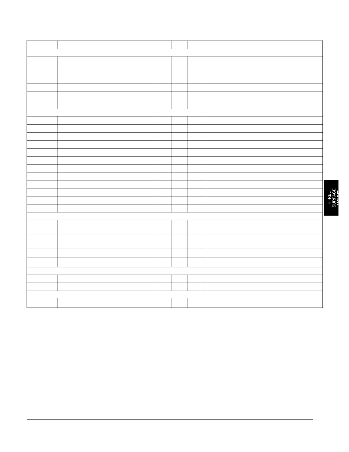
Elec tri cal Char ac ter ics (TA = 25o C un less oth er wise noted)
SYM BOL PA RAME TER MIN MAX UNITS TEST CON DI TIONS
Off Char ac ter is tics
V
(BR)CBO
V
(BR)CEO
V
(BR)EBO
I
CBO
I
CBO2
I
EBO
On Char ac ter is tics
h
FE1
h
FE2
h
FE3
h
FE4
h
FE5
h
FE6
V
CE(SAT)1
V
CE(SAT)2
V
CE(SAT)3
V
BE(SAT)1
V
BE(SAT)2
V
BE(SAT)3
Small- Signal Char ac ter is tics
h
h
C
obo
C
ibo
Switch ing Chara ter is tics
t
on
t
off
Tran sis tor to Tran sis tor Iso la tion
R
Collector-Base Breakdown Voltage 75
Collector-Emitter Breakdown Voltage 50 V IC = 10 mA
Emitter-Base Breakdown Voltage 6
V
V
IC = 10 µA
(2)
IE = 10 µA
Collector-Base Cutoff Current 10 nA VCB = 60 V
Collector-Base Cutoff Current
10
VCB = 60 V, TA = 150o C
µA
Emitter-Base Cutoff Current 10 nA VEB = 4 V
Forward Current Transfer Ratio 50 VCE = 10 V, IC = 0.1 mA
Forward Current Transfer Ratio 75 325 VCE = 10 V, IC = 1.0 mA
Forward Current Transfer Ratio 100 VCE = 10 V, IC = 10 mA
Forward Current Transfer Ratio 100 300 VCE = 10 V, IC = 150 mA
Forward Current Transfer Ratio 30 VCE = 10 V, IC = 500 mA
(2)
(2)
(2)
Forward Current Transfer Ratio 35 VCE = 10 V, IC = 10 mA, TA = 55o C
Collector-Emitter Saturation Voltage 0.3 V IC = 150 mA, IB = 15 mA
Collector-Emitter Saturation Voltage 1.0 V IC = 500 mA, IB = 50 mA
(2)
(2)
Collector-Emitter Saturation Voltage 0.45 V IC = 150 mA, IB = 15 mA, TA = 150o C
Base-Emitter Saturation Voltage 0.6 1.2 V IC = 150 mA, IB = 15 mA
Base-Emitter Saturation Voltage 2.0 V IC = 500 mA, IB = 50 mA
(2)
(2)
Base-Emitter Saturation Voltage 1.4 V IC = 150 mA, IB = 15 mA, TA = 55o C
Magnitude of Small-Signal Short-Circuit
fe
Forward Current Transfer Ratio
Small-Signal Short Circuit Forward
fe
Current Transfer Ratio
Open Circuit Output Capacitance
Input Capacitance
2.5 8.0
50
8 pF
33 pF
VCE = 10 V, IC = 20 mA, f = 100 MHz
VCE = 10 V, IC = 1 mA, f = 1kHz
VCB = 10 V, IE = 0, 100 kHz ≤ f ≤ 1 MHz
VEB = 0.5 V, IC = 0, 100 kHz ≤ f ≤ 1 MHz
Turn-On Time 35 ns VCC = 30 V, IC = 150 mA, IB = 15 mA
Turn-Off Time 300 ns VCC = 30 V, IC = 150 mA, IB1 = IB2 = 15 mA
Isolation Resistance
t-t
10k
MΩ
V
= 500 V
t-t
(2)
(2)
(2)
(2) Pulsed Test: Pulse Width = 300 µs ±50, 1-2 % Duty Cycle.
Optek Technology, Inc. 1215 W. Crosby Road Carrollton, Texas 75006 (972)323-2200 Fax (972)323-2396
15-21
 Loading...