

Page 1

OPTOMMP PROTOCOL GUIDE
Used with:
groov EPIC Processors
groov RIO modules
SNAP PAC R-Series Controllers
SNAP PAC S-Series Controllers
SNAP PAC EB Brains
SNAP PAC SB Brains
SNAP Simple I/O™
SNAP Ethernet I/O™
SNAP Ultimate I/O™
SNAP-LCE Controller
E1 Brain Board
E2 Brain Board
G4EB2 Brain Boards
Form 1465-200714—July 2020
Page 2

OptoMMP Protocol Guide
Form 1465-200714—July 2020
Copyright © 2003–2020 Opto 22.
All rights reserved.
Printed in the United States of America.
The information in this manual has been checked carefully and is believed to be accurate; however, Opto 22 assumes no
responsibility for possible inaccuracies or omissions. Specifications are subject to change without notice.
Opto 22 warrants all of its products to be free from defects in material or workmanship for 30 months from the
manufacturing date code. This warranty is limited to the original cost of the unit only and does not cover installation, labor,
or any other contingent costs. Opto 22 I/O modules and solid-state relays with date codes of 1/96 or newer are guaranteed
for life. This lifetime warranty excludes reed relay modules, groov and SNAP serial communication modules, SNAP PID
modules, and modules that contain mechanical contacts or switches. Opto 22 does not warrant any product, components,
or parts not manufactured by Opto 22; for these items, the warranty from the original manufacturer applies. Refer to Opto
22 form 1042 for complete warranty information.
Wired+Wireless controllers and brains are licensed under one or more of the following patents: U.S. Patent No(s). 5282222,
RE37802, 6963617; Canadian Patent No. 2064975; European Patent No. 1142245; French Patent No. 1142245; British Patent
No. 1142245; Japanese Patent No. 2002535925A; German Patent No. 60011224.
Opto 22 FactoryFloor, groov, groov EPIC, groov RIO, mobile made simple, Optomux, and Pamux are registered trademarks of
Opto 22. Generation 4, groov Server, ioControl, ioDisplay, ioManager, ioProject, ioUtilities, mistic, Nvio, Nvio.net Web Portal,
OptoConnect, OptoControl, OptoDataLink, OptoDisplay, OptoEMU, OptoEMU Sensor, OptoEMU Server, OptoOPCServer,
OptoScript, OptoServer, OptoTerminal, OptoUtilities, PAC Control, PAC Display, PAC Manager, PAC Project, PAC Project Basic,
PAC Project Professional, SNAP Ethernet I/O, SNAP I/O, SNAP OEM I/O, SNAP PAC System, SNAP Simple I/O, SNAP Ultimate
I/O, and Wired+Wireless are trademarks of Opto 22.
ActiveX, JScript, Microsoft, MS-DOS, VBScript, Visual Basic, Visual C++, Windows, and Windows Vista are either registered
trademarks or trademarks of Microsoft Corporation in the United States and other countries. Linux is a registered
trademark of Linus Torvalds. ARCNET is a registered trademark of Datapoint Corporation. Modbus is a registered trademark
of Schneider Electric, licensed to the Modbus Organization, Inc. Wiegand is a registered trademark of Sensor Engineering
Corporation. Allen-Bradley, CompactLogix, ControlLogix, MicroLogix, SLC, and RSLogix are either registered trademarks or
trademarks of Rockwell Automation. CIP and EtherNet/IP are trademarks of ODVA. Raspberry Pi is a trademark of the
Raspberry Pi Foundation. The registered trademark Ignition by Inductive Automation® is owned by Inductive Automation
and is registered in the United States and may be pending or registered in other countries. CODESYS® is a registered
trademark of 3S-Smart Software Solutions GmbH.
groov includes software developed by the OpenSSL Project for use in the OpenSSL Toolkit. (http://www.openssl.org)
All other brand or product names are trademarks or registered trademarks of their respective companies or organizations.
ii
OptoMMP Protocol Guide
Opto 22
Automation Made Simple.
Page 3

Table of Contents
Chapter 1: Introduction . . . . . . . . . . . . . . . . . . . . . . . . . . . . . . . . . . . . . . . . . . . . . . . . . . . . . . . . .1
Welcome to OptoMMP. . . . . . . . . . . . . . . . . . . . . . . . . . . . . . . . . . . . . . . . . . . . . . . . . . . . . . . . . . . . . . . . . . . . . . . . . . . . . 1
About this Guide. . . . . . . . . . . . . . . . . . . . . . . . . . . . . . . . . . . . . . . . . . . . . . . . . . . . . . . . . . . . . . . . . . . . . . . . . . . . . . . . . . . 2
Information Key . . . . . . . . . . . . . . . . . . . . . . . . . . . . . . . . . . . . . . . . . . . . . . . . . . . . . . . . . . . . . . . . . . . . . . . . . . . . . . 2
Other Documents You May Need . . . . . . . . . . . . . . . . . . . . . . . . . . . . . . . . . . . . . . . . . . . . . . . . . . . . . . . . . . . . . . 3
For Help . . . . . . . . . . . . . . . . . . . . . . . . . . . . . . . . . . . . . . . . . . . . . . . . . . . . . . . . . . . . . . . . . . . . . . . . . . . . . . . . . . . . . . . . . . . 3
Chapter 2: Overview of Programming . . . . . . . . . . . . . . . . . . . . . . . . . . . . . . . . . . . . . . . . . . . 5
Introduction . . . . . . . . . . . . . . . . . . . . . . . . . . . . . . . . . . . . . . . . . . . . . . . . . . . . . . . . . . . . . . . . . . . . . . . . . . . . . . . . . . . . . . . 5
Programming Steps for Opto 22 Devices . . . . . . . . . . . . . . . . . . . . . . . . . . . . . . . . . . . . . . . . . . . . . . . . . . . . . . . . . . . . 5
Communication Options . . . . . . . . . . . . . . . . . . . . . . . . . . . . . . . . . . . . . . . . . . . . . . . . . . . . . . . . . . . . . . . . . . . . . . . . . . . 6
Communication Options that Do Not Require the OptoMMP Protocol . . . . . . . . . . . . . . . . . . . . . . . . . . . 6
Accessing Opto 22 Ethernet-Based Devices over the internet . . . . . . . . . . . . . . . . . . . . . . . . . . . . . . . . . . . 6
CAUTION: Multiple Communication Options Can Cause Conflict . . . . . . . . . . . . . . . . . . . . . . . . . . . . . . . . 7
Understanding the Memory Map . . . . . . . . . . . . . . . . . . . . . . . . . . . . . . . . . . . . . . . . . . . . . . . . . . . . . . . . . . . . . . . . . . . 8
Referencing Module and Channel Positions on I/O Units . . . . . . . . . . . . . . . . . . . . . . . . . . . . . . . . . . . . . . . . . . . . . 9
groov I/O Units . . . . . . . . . . . . . . . . . . . . . . . . . . . . . . . . . . . . . . . . . . . . . . . . . . . . . . . . . . . . . . . . . . . . . . . . . . . . . . . 9
groov RIO Units . . . . . . . . . . . . . . . . . . . . . . . . . . . . . . . . . . . . . . . . . . . . . . . . . . . . . . . . . . . . . . . . . . . . . . . . . . . . . . 10
SNAP I/O Units . . . . . . . . . . . . . . . . . . . . . . . . . . . . . . . . . . . . . . . . . . . . . . . . . . . . . . . . . . . . . . . . . . . . . . . . . . . . . . 11
SNAP B-Series I/O Units . . . . . . . . . . . . . . . . . . . . . . . . . . . . . . . . . . . . . . . . . . . . . . . . . . . . . . . . . . . . . . . . . . . . . . 11
SNAP Digital-Only I/O Units . . . . . . . . . . . . . . . . . . . . . . . . . . . . . . . . . . . . . . . . . . . . . . . . . . . . . . . . . . . . . . . . . . 12
E1 and E2 I/O Units . . . . . . . . . . . . . . . . . . . . . . . . . . . . . . . . . . . . . . . . . . . . . . . . . . . . . . . . . . . . . . . . . . . . . . . . . . 13
G4EB2 I/O Units . . . . . . . . . . . . . . . . . . . . . . . . . . . . . . . . . . . . . . . . . . . . . . . . . . . . . . . . . . . . . . . . . . . . . . . . . . . . . 14
Configuring I/O Channels. . . . . . . . . . . . . . . . . . . . . . . . . . . . . . . . . . . . . . . . . . . . . . . . . . . . . . . . . . . . . . . . . . . . . . . . . . 16
Configuring I/O Channels for groov I/O Units . . . . . . . . . . . . . . . . . . . . . . . . . . . . . . . . . . . . . . . . . . . . . . . . . . 16
Configuring I/O Channels for groov RIO Units . . . . . . . . . . . . . . . . . . . . . . . . . . . . . . . . . . . . . . . . . . . . . . . . . . 20
Configuring I/O Channels for SNAP Analog/Digital I/O Units . . . . . . . . . . . . . . . . . . . . . . . . . . . . . . . . . . . 21
Configuring Channel Features . . . . . . . . . . . . . . . . . . . . . . . . . . . . . . . . . . . . . . . . . . . . . . . . . . . . . . . . . . . . . . . . . . . . . 31
Selecting Configuration Values for I/O Channel Features . . . . . . . . . . . . . . . . . . . . . . . . . . . . . . . . . . . . . . . 31
States (Digital Channels) . . . . . . . . . . . . . . . . . . . . . . . . . . . . . . . . . . . . . . . . . . . . . . . . . . . . . . . . . . . . . . . . . . . . . 32
Latches (Digital Channels) . . . . . . . . . . . . . . . . . . . . . . . . . . . . . . . . . . . . . . . . . . . . . . . . . . . . . . . . . . . . . . . . . . . . 33
Counters (Digital Channels) . . . . . . . . . . . . . . . . . . . . . . . . . . . . . . . . . . . . . . . . . . . . . . . . . . . . . . . . . . . . . . . . . . 33
Quadrature Counters (Digital Inputs) . . . . . . . . . . . . . . . . . . . . . . . . . . . . . . . . . . . . . . . . . . . . . . . . . . . . . . . . . . 34
Pulse Measurement (Digital Inputs) . . . . . . . . . . . . . . . . . . . . . . . . . . . . . . . . . . . . . . . . . . . . . . . . . . . . . . . . . . . 34
Frequency or Period Measurement (Digital Inputs) . . . . . . . . . . . . . . . . . . . . . . . . . . . . . . . . . . . . . . . . . . . . 35
OptoMMP Protocol Guide iii
iii
Page 4

Digital Totalizer . . . . . . . . . . . . . . . . . . . . . . . . . . . . . . . . . . . . . . . . . . . . . . . . . . . . . . . . . . . . . . . . . . . . . . . . . . . . . . 35
Watchdog (Digital and Analog Channels) . . . . . . . . . . . . . . . . . . . . . . . . . . . . . . . . . . . . . . . . . . . . . . . . . . . . . 36
Scaling (Analog Channels) . . . . . . . . . . . . . . . . . . . . . . . . . . . . . . . . . . . . . . . . . . . . . . . . . . . . . . . . . . . . . . . . . . . 36
Minimum and Maximum Values (Analog Channels) . . . . . . . . . . . . . . . . . . . . . . . . . . . . . . . . . . . . . . . . . . . 37
Offset and Gain (Analog Channels) . . . . . . . . . . . . . . . . . . . . . . . . . . . . . . . . . . . . . . . . . . . . . . . . . . . . . . . . . . . 37
Clamping (Analog Channels) . . . . . . . . . . . . . . . . . . . . . . . . . . . . . . . . . . . . . . . . . . . . . . . . . . . . . . . . . . . . . . . . . 37
Average Filter Weight (Analog Channels) . . . . . . . . . . . . . . . . . . . . . . . . . . . . . . . . . . . . . . . . . . . . . . . . . . . . . 37
Scratch Pad . . . . . . . . . . . . . . . . . . . . . . . . . . . . . . . . . . . . . . . . . . . . . . . . . . . . . . . . . . . . . . . . . . . . . . . . . . . . . . . . . 38
Using Scratch Pad Bits for Events and Alarms . . . . . . . . . . . . . . . . . . . . . . . . . . . . . . . . . . . . . . . . . . . . . . . . . . 39
Types of Events, Alarms, and Reactions . . . . . . . . . . . . . . . . . . . . . . . . . . . . . . . . . . . . . . . . . . . . . . . . . . . . . . . 39
Steps for Configuring Events and Reactions—PAC Firmware R8.1 and Higher . . . . . . . . . . . . . . . . . . 41
Steps for Configuring Events and Reactions—PAC Firmware R8.0 and Lower . . . . . . . . . . . . . . . . . . . 42
Using Digital Events and Reactions . . . . . . . . . . . . . . . . . . . . . . . . . . . . . . . . . . . . . . . . . . . . . . . . . . . . . . . . . . . 44
Using Alarms and Reactions . . . . . . . . . . . . . . . . . . . . . . . . . . . . . . . . . . . . . . . . . . . . . . . . . . . . . . . . . . . . . . . . . . 48
Using Serial Events and Reactions . . . . . . . . . . . . . . . . . . . . . . . . . . . . . . . . . . . . . . . . . . . . . . . . . . . . . . . . . . . . 49
Using SNMP in Reactions . . . . . . . . . . . . . . . . . . . . . . . . . . . . . . . . . . . . . . . . . . . . . . . . . . . . . . . . . . . . . . . . . . . . 49
Setting Up Event Messages . . . . . . . . . . . . . . . . . . . . . . . . . . . . . . . . . . . . . . . . . . . . . . . . . . . . . . . . . . . . . . . . . . 50
Using Email . . . . . . . . . . . . . . . . . . . . . . . . . . . . . . . . . . . . . . . . . . . . . . . . . . . . . . . . . . . . . . . . . . . . . . . . . . . . . . . . . 50
Using Plugins . . . . . . . . . . . . . . . . . . . . . . . . . . . . . . . . . . . . . . . . . . . . . . . . . . . . . . . . . . . . . . . . . . . . . . . . . . . . . . . 50
Streaming Data . . . . . . . . . . . . . . . . . . . . . . . . . . . . . . . . . . . . . . . . . . . . . . . . . . . . . . . . . . . . . . . . . . . . . . . . . . . . . . . . . . . 51
Traditional Streaming . . . . . . . . . . . . . . . . . . . . . . . . . . . . . . . . . . . . . . . . . . . . . . . . . . . . . . . . . . . . . . . . . . . . . . . . 52
Custom Streaming . . . . . . . . . . . . . . . . . . . . . . . . . . . . . . . . . . . . . . . . . . . . . . . . . . . . . . . . . . . . . . . . . . . . . . . . . . 53
Logging Data . . . . . . . . . . . . . . . . . . . . . . . . . . . . . . . . . . . . . . . . . . . . . . . . . . . . . . . . . . . . . . . . . . . . . . . . . . . . . . . . . . . . . 54
Configuring the Event and Memory Map Addresses to Log . . . . . . . . . . . . . . . . . . . . . . . . . . . . . . . . . . . . 54
Reading the Data from the Data Log . . . . . . . . . . . . . . . . . . . . . . . . . . . . . . . . . . . . . . . . . . . . . . . . . . . . . . . . . . 55
Using PID Loops . . . . . . . . . . . . . . . . . . . . . . . . . . . . . . . . . . . . . . . . . . . . . . . . . . . . . . . . . . . . . . . . . . . . . . . . . . . . . . . . . . 55
What is a PID? . . . . . . . . . . . . . . . . . . . . . . . . . . . . . . . . . . . . . . . . . . . . . . . . . . . . . . . . . . . . . . . . . . . . . . . . . . . . . . . 55
PID Loops on Ethernet-based I/O Units . . . . . . . . . . . . . . . . . . . . . . . . . . . . . . . . . . . . . . . . . . . . . . . . . . . . . . . 55
Algorithm Choices . . . . . . . . . . . . . . . . . . . . . . . . . . . . . . . . . . . . . . . . . . . . . . . . . . . . . . . . . . . . . . . . . . . . . . . . . . . 57
Formatting and Interpreting Data. . . . . . . . . . . . . . . . . . . . . . . . . . . . . . . . . . . . . . . . . . . . . . . . . . . . . . . . . . . . . . . . . . 58
Mask Data . . . . . . . . . . . . . . . . . . . . . . . . . . . . . . . . . . . . . . . . . . . . . . . . . . . . . . . . . . . . . . . . . . . . . . . . . . . . . . . . . . . 58
Unsigned 32-bit Integer Data . . . . . . . . . . . . . . . . . . . . . . . . . . . . . . . . . . . . . . . . . . . . . . . . . . . . . . . . . . . . . . . . 59
Digital Channel Data (4-Channel Modules) . . . . . . . . . . . . . . . . . . . . . . . . . . . . . . . . . . . . . . . . . . . . . . . . . . . . 60
IEEE Float Data . . . . . . . . . . . . . . . . . . . . . . . . . . . . . . . . . . . . . . . . . . . . . . . . . . . . . . . . . . . . . . . . . . . . . . . . . . . . . . 61
Analog Bank Data . . . . . . . . . . . . . . . . . . . . . . . . . . . . . . . . . . . . . . . . . . . . . . . . . . . . . . . . . . . . . . . . . . . . . . . . . . . 61
iv
Chapter 3: Using OptoMMP Software Development Kits . . . . . . . . . . . . . . . . . . . . . . . . . 63
Introduction . . . . . . . . . . . . . . . . . . . . . . . . . . . . . . . . . . . . . . . . . . . . . . . . . . . . . . . . . . . . . . . . . . . . . . . . . . . . . . . . . . . . . . 63
C++ OptoMMP Software Development Kit for groov EPIC, groov RIO, and SNAP PAC . . . . . . . . . . . . . . . . . 63
A Few Examples . . . . . . . . . . . . . . . . . . . . . . . . . . . . . . . . . . . . . . . . . . . . . . . . . . . . . . . . . . . . . . . . . . . . . . . . . . . . . 63
.NET OptoMMP Software Development Kit for groov EPIC, groov RIO, and SNAP PAC . . . . . . . . . . . . . . . . . 64
Chapter 4: Using the OptoMMP Protocol . . . . . . . . . . . . . . . . . . . . . . . . . . . . . . . . . . . . . . . 65
Introduction . . . . . . . . . . . . . . . . . . . . . . . . . . . . . . . . . . . . . . . . . . . . . . . . . . . . . . . . . . . . . . . . . . . . . . . . . . . . . . . . . . . . . . 65
Memory Mapping . . . . . . . . . . . . . . . . . . . . . . . . . . . . . . . . . . . . . . . . . . . . . . . . . . . . . . . . . . . . . . . . . . . . . . . . . . . . . . . . 66
Communication Packets . . . . . . . . . . . . . . . . . . . . . . . . . . . . . . . . . . . . . . . . . . . . . . . . . . . . . . . . . . . . . . . . . . . . . 66
Overview of Custom Application Programming . . . . . . . . . . . . . . . . . . . . . . . . . . . . . . . . . . . . . . . . . . . . . . . . . . . . 67
Connecting . . . . . . . . . . . . . . . . . . . . . . . . . . . . . . . . . . . . . . . . . . . . . . . . . . . . . . . . . . . . . . . . . . . . . . . . . . . . . . . . . 67
OptoMMP Protocol Guide
Page 5

Sending Powerup Clear . . . . . . . . . . . . . . . . . . . . . . . . . . . . . . . . . . . . . . . . . . . . . . . . . . . . . . . . . . . . . . . . . . . . . . 68
Configuring . . . . . . . . . . . . . . . . . . . . . . . . . . . . . . . . . . . . . . . . . . . . . . . . . . . . . . . . . . . . . . . . . . . . . . . . . . . . . . . . . 69
Reading and Writing . . . . . . . . . . . . . . . . . . . . . . . . . . . . . . . . . . . . . . . . . . . . . . . . . . . . . . . . . . . . . . . . . . . . . . . . . 70
Disconnecting . . . . . . . . . . . . . . . . . . . . . . . . . . . . . . . . . . . . . . . . . . . . . . . . . . . . . . . . . . . . . . . . . . . . . . . . . . . . . . . 71
Streaming Data . . . . . . . . . . . . . . . . . . . . . . . . . . . . . . . . . . . . . . . . . . . . . . . . . . . . . . . . . . . . . . . . . . . . . . . . . . . . . . . . . . . 72
Configuring Parameters for Streaming . . . . . . . . . . . . . . . . . . . . . . . . . . . . . . . . . . . . . . . . . . . . . . . . . . . . . . . . 72
Receiving Streamed Data . . . . . . . . . . . . . . . . . . . . . . . . . . . . . . . . . . . . . . . . . . . . . . . . . . . . . . . . . . . . . . . . . . . . 72
Configuring I/O Channels and Features . . . . . . . . . . . . . . . . . . . . . . . . . . . . . . . . . . . . . . . . . . . . . . . . . . . . . . . . . . . . 72
Reading Module Types . . . . . . . . . . . . . . . . . . . . . . . . . . . . . . . . . . . . . . . . . . . . . . . . . . . . . . . . . . . . . . . . . . . . . . . 72
Configuring I/O Channel Types . . . . . . . . . . . . . . . . . . . . . . . . . . . . . . . . . . . . . . . . . . . . . . . . . . . . . . . . . . . . . . . 73
Using I/O Channel Features. . . . . . . . . . . . . . . . . . . . . . . . . . . . . . . . . . . . . . . . . . . . . . . . . . . . . . . . . . . . . . . . . . . . . . . . 73
Latches . . . . . . . . . . . . . . . . . . . . . . . . . . . . . . . . . . . . . . . . . . . . . . . . . . . . . . . . . . . . . . . . . . . . . . . . . . . . . . . . . . . . . 73
Counters . . . . . . . . . . . . . . . . . . . . . . . . . . . . . . . . . . . . . . . . . . . . . . . . . . . . . . . . . . . . . . . . . . . . . . . . . . . . . . . . . . . . 74
Quadrature Counters . . . . . . . . . . . . . . . . . . . . . . . . . . . . . . . . . . . . . . . . . . . . . . . . . . . . . . . . . . . . . . . . . . . . . . . . 74
Watchdog . . . . . . . . . . . . . . . . . . . . . . . . . . . . . . . . . . . . . . . . . . . . . . . . . . . . . . . . . . . . . . . . . . . . . . . . . . . . . . . . . . . 75
Scaling . . . . . . . . . . . . . . . . . . . . . . . . . . . . . . . . . . . . . . . . . . . . . . . . . . . . . . . . . . . . . . . . . . . . . . . . . . . . . . . . . . . . . . 75
Minimum and Maximum Values . . . . . . . . . . . . . . . . . . . . . . . . . . . . . . . . . . . . . . . . . . . . . . . . . . . . . . . . . . . . . . 75
Offset/Gain . . . . . . . . . . . . . . . . . . . . . . . . . . . . . . . . . . . . . . . . . . . . . . . . . . . . . . . . . . . . . . . . . . . . . . . . . . . . . . . . . . 76
Read and Write Packet Structure . . . . . . . . . . . . . . . . . . . . . . . . . . . . . . . . . . . . . . . . . . . . . . . . . . . . . . . . . . . . . . . . . . . 76
Parameters . . . . . . . . . . . . . . . . . . . . . . . . . . . . . . . . . . . . . . . . . . . . . . . . . . . . . . . . . . . . . . . . . . . . . . . . . . . . . . . . . . 76
Packet Structure . . . . . . . . . . . . . . . . . . . . . . . . . . . . . . . . . . . . . . . . . . . . . . . . . . . . . . . . . . . . . . . . . . . . . . . . . . . . . 77
Error Codes . . . . . . . . . . . . . . . . . . . . . . . . . . . . . . . . . . . . . . . . . . . . . . . . . . . . . . . . . . . . . . . . . . . . . . . . . . . . . . . . . . . . . . . 80
Appendix A: Opto 22 Hardware Memory Map . . . . . . . . . . . . . . . . . . . . . . . . . . . . . . . . . . 81
Introduction . . . . . . . . . . . . . . . . . . . . . . . . . . . . . . . . . . . . . . . . . . . . . . . . . . . . . . . . . . . . . . . . . . . . . . . . . . . . . . . . . . . . . . 81
Notes on Columns . . . . . . . . . . . . . . . . . . . . . . . . . . . . . . . . . . . . . . . . . . . . . . . . . . . . . . . . . . . . . . . . . . . . . . . . . . . . . . . . 83
Byte Ordering and Data Ordering . . . . . . . . . . . . . . . . . . . . . . . . . . . . . . . . . . . . . . . . . . . . . . . . . . . . . . . . . . . . . . . . . . 83
For Experienced OptoMMP Users . . . . . . . . . . . . . . . . . . . . . . . . . . . . . . . . . . . . . . . . . . . . . . . . . . . . . . . . . . . . . . . . . . 84
General Notes . . . . . . . . . . . . . . . . . . . . . . . . . . . . . . . . . . . . . . . . . . . . . . . . . . . . . . . . . . . . . . . . . . . . . . . . . . . . . . . . . . . . 84
(Expanded) Analog & Digital Channel Configuration—Read/Write. . . . . . . . . . . . . . . . . . . . . . . . . . . . . . . . . . . 85
(Expanded) Analog Channel Calc & Set—Read/Write . . . . . . . . . . . . . . . . . . . . . . . . . . . . . . . . . . . . . . . . . . . . . . . 87
(Expanded) Analog Channel Read & Clear—Read/Write . . . . . . . . . . . . . . . . . . . . . . . . . . . . . . . . . . . . . . . . . . . . 87
(Expanded) Analog Channel Read—Read Only . . . . . . . . . . . . . . . . . . . . . . . . . . . . . . . . . . . . . . . . . . . . . . . . . . . . . 88
(Expanded) Analog Channel Write—Read/Write. . . . . . . . . . . . . . . . . . . . . . . . . . . . . . . . . . . . . . . . . . . . . . . . . . . . 89
(Expanded) Digital Channel Read—Read Only. . . . . . . . . . . . . . . . . . . . . . . . . . . . . . . . . . . . . . . . . . . . . . . . . . . . . . 89
(Expanded) Digital Channel—Read/Write . . . . . . . . . . . . . . . . . . . . . . . . . . . . . . . . . . . . . . . . . . . . . . . . . . . . . . . . . . 90
(Expanded) Digital Channel Read & Clear—Read Only . . . . . . . . . . . . . . . . . . . . . . . . . . . . . . . . . . . . . . . . . . . . . . 90
(Expanded) Digital Packed Data—Read Only . . . . . . . . . . . . . . . . . . . . . . . . . . . . . . . . . . . . . . . . . . . . . . . . . . . . . . . 91
(Expanded) Digital Packed Must on/OFF (MOMO)—Read/Write . . . . . . . . . . . . . . . . . . . . . . . . . . . . . . . . . . . . . 91
Status Area Read—Read Only . . . . . . . . . . . . . . . . . . . . . . . . . . . . . . . . . . . . . . . . . . . . . . . . . . . . . . . . . . . . . . . . . . . . . 92
Module Build Data–Read Only . . . . . . . . . . . . . . . . . . . . . . . . . . . . . . . . . . . . . . . . . . . . . . . . . . . . . . . . . . . . . . . . . . . . . 96
Quality of Data–Read Only. . . . . . . . . . . . . . . . . . . . . . . . . . . . . . . . . . . . . . . . . . . . . . . . . . . . . . . . . . . . . . . . . . . . . . . . . 97
Communications Port Configuration—Read/Write . . . . . . . . . . . . . . . . . . . . . . . . . . . . . . . . . . . . . . . . . . . . . . . . . 97
Serial Pass-Through—Read/Write . . . . . . . . . . . . . . . . . . . . . . . . . . . . . . . . . . . . . . . . . . . . . . . . . . . . . . . . . . . . . . . 100
Date and Time Configuration—Read/Write . . . . . . . . . . . . . . . . . . . . . . . . . . . . . . . . . . . . . . . . . . . . . . . . . . . . . . 101
Status Area Write—Read/Write . . . . . . . . . . . . . . . . . . . . . . . . . . . . . . . . . . . . . . . . . . . . . . . . . . . . . . . . . . . . . . . . . . 101
Modbus Configuration—Read/Write. . . . . . . . . . . . . . . . . . . . . . . . . . . . . . . . . . . . . . . . . . . . . . . . . . . . . . . . . . . . . 104
OptoMMP Protocol Guide
v
Page 6

Network Security Configuration—Read/Write . . . . . . . . . . . . . . . . . . . . . . . . . . . . . . . . . . . . . . . . . . . . . . . . . . . . . 104
SSI Module Configuration—Read/Write. . . . . . . . . . . . . . . . . . . . . . . . . . . . . . . . . . . . . . . . . . . . . . . . . . . . . . . . . . . 105
Serial Module Identification—Read Only . . . . . . . . . . . . . . . . . . . . . . . . . . . . . . . . . . . . . . . . . . . . . . . . . . . . . . . . . . 106
Serial Module Configuration—Read/Write . . . . . . . . . . . . . . . . . . . . . . . . . . . . . . . . . . . . . . . . . . . . . . . . . . . . . . . . 107
Serial Module and Port Numbers . . . . . . . . . . . . . . . . . . . . . . . . . . . . . . . . . . . . . . . . . . . . . . . . . . . . . . . . . . . . 108
Wiegand Serial Module Configuration—Read/Write . . . . . . . . . . . . . . . . . . . . . . . . . . . . . . . . . . . . . . . . . . . . . . . 108
Wiegand Module and Port Numbers . . . . . . . . . . . . . . . . . . . . . . . . . . . . . . . . . . . . . . . . . . . . . . . . . . . . . . . . . 109
SNAP-SCM-CAN2B Serial Module Configuration—Read/Write . . . . . . . . . . . . . . . . . . . . . . . . . . . . . . . . . . . . . 110
SNAP-SCM-CAN2B Module and Port Numbers . . . . . . . . . . . . . . . . . . . . . . . . . . . . . . . . . . . . . . . . . . . . . . . 112
HART Module Configuration—Read/Write . . . . . . . . . . . . . . . . . . . . . . . . . . . . . . . . . . . . . . . . . . . . . . . . . . . . . . . . 112
HART Module and Port Numbers . . . . . . . . . . . . . . . . . . . . . . . . . . . . . . . . . . . . . . . . . . . . . . . . . . . . . . . . . . . . 113
SNMP Configuration—Read/Write. . . . . . . . . . . . . . . . . . . . . . . . . . . . . . . . . . . . . . . . . . . . . . . . . . . . . . . . . . . . . . . . 114
FTP User Name/Password Configuration—Read/Write. . . . . . . . . . . . . . . . . . . . . . . . . . . . . . . . . . . . . . . . . . . . . 115
PPP Configuration—Read/Write. . . . . . . . . . . . . . . . . . . . . . . . . . . . . . . . . . . . . . . . . . . . . . . . . . . . . . . . . . . . . . . . . . 115
PPP Status—Read Only . . . . . . . . . . . . . . . . . . . . . . . . . . . . . . . . . . . . . . . . . . . . . . . . . . . . . . . . . . . . . . . . . . . . . . . . . . 118
Streaming Configuration—Read/Write . . . . . . . . . . . . . . . . . . . . . . . . . . . . . . . . . . . . . . . . . . . . . . . . . . . . . . . . . . . 119
Digital Bank Read—Read Only. . . . . . . . . . . . . . . . . . . . . . . . . . . . . . . . . . . . . . . . . . . . . . . . . . . . . . . . . . . . . . . . . . . . 119
Digital Bank Write—Read/Write . . . . . . . . . . . . . . . . . . . . . . . . . . . . . . . . . . . . . . . . . . . . . . . . . . . . . . . . . . . . . . . . . . 120
Analog Bank Read—Read Only . . . . . . . . . . . . . . . . . . . . . . . . . . . . . . . . . . . . . . . . . . . . . . . . . . . . . . . . . . . . . . . . . . . 120
Analog Bank Write—Read/Write . . . . . . . . . . . . . . . . . . . . . . . . . . . . . . . . . . . . . . . . . . . . . . . . . . . . . . . . . . . . . . . . . 121
Digital Channel Read—Read Only . . . . . . . . . . . . . . . . . . . . . . . . . . . . . . . . . . . . . . . . . . . . . . . . . . . . . . . . . . . . . . . . 121
Digital Channel Write—Read/Write. . . . . . . . . . . . . . . . . . . . . . . . . . . . . . . . . . . . . . . . . . . . . . . . . . . . . . . . . . . . . . . 122
(Old) Analog Channel Read—Read Only . . . . . . . . . . . . . . . . . . . . . . . . . . . . . . . . . . . . . . . . . . . . . . . . . . . . . . . . . . 123
(Old) Analog Channel Write—Read/Write. . . . . . . . . . . . . . . . . . . . . . . . . . . . . . . . . . . . . . . . . . . . . . . . . . . . . . . . . 123
(Old) Analog and Digital Channel Configuration Information—Read/Write . . . . . . . . . . . . . . . . . . . . . . . . . 124
(Old) Digital Events and Reactions—Read/Write. . . . . . . . . . . . . . . . . . . . . . . . . . . . . . . . . . . . . . . . . . . . . . . . . . . 127
Digital Events - Expanded (formerly Timers)—Read/Write . . . . . . . . . . . . . . . . . . . . . . . . . . . . . . . . . . . . . . . . . 127
Addresses for SNAP Firmware R8.1 and Higher . . . . . . . . . . . . . . . . . . . . . . . . . . . . . . . . . . . . . . . . . . . . . . . 127
Addresses for SNAP Firmware R8.0 and Lower . . . . . . . . . . . . . . . . . . . . . . . . . . . . . . . . . . . . . . . . . . . . . . . 132
Custom Configuration Area—Write. . . . . . . . . . . . . . . . . . . . . . . . . . . . . . . . . . . . . . . . . . . . . . . . . . . . . . . . . . . . . . . 133
Custom Data Access Area—Read/Write. . . . . . . . . . . . . . . . . . . . . . . . . . . . . . . . . . . . . . . . . . . . . . . . . . . . . . . . . . . 134
Scratch Pad—Read/Write . . . . . . . . . . . . . . . . . . . . . . . . . . . . . . . . . . . . . . . . . . . . . . . . . . . . . . . . . . . . . . . . . . . . . . . . 134
(Old) Analog Channel Calculation and Set—Read Only . . . . . . . . . . . . . . . . . . . . . . . . . . . . . . . . . . . . . . . . . . . . 136
(Old) Digital Read and Clear—Read Only. . . . . . . . . . . . . . . . . . . . . . . . . . . . . . . . . . . . . . . . . . . . . . . . . . . . . . . . . . 136
(Old) Analog Read and Clear/Restart—Read Only . . . . . . . . . . . . . . . . . . . . . . . . . . . . . . . . . . . . . . . . . . . . . . . . . 137
Streaming—Read Only . . . . . . . . . . . . . . . . . . . . . . . . . . . . . . . . . . . . . . . . . . . . . . . . . . . . . . . . . . . . . . . . . . . . . . . . . . 138
Addresses for PR1 and RIO . . . . . . . . . . . . . . . . . . . . . . . . . . . . . . . . . . . . . . . . . . . . . . . . . . . . . . . . . . . . . . . . . . 138
Addresses for PAC-R, EB, UIO, EIO, SIO, and G4EB2 Devices . . . . . . . . . . . . . . . . . . . . . . . . . . . . . . . . . . . . 138
Analog EU or Digital Counter (Feature) Packed Data—Read. . . . . . . . . . . . . . . . . . . . . . . . . . . . . . . . . . . . . . . . 139
Digital Packed Data—Read/Write. . . . . . . . . . . . . . . . . . . . . . . . . . . . . . . . . . . . . . . . . . . . . . . . . . . . . . . . . . . . . . . . . 139
Alarm Event Settings—Read/Write . . . . . . . . . . . . . . . . . . . . . . . . . . . . . . . . . . . . . . . . . . . . . . . . . . . . . . . . . . . . . . . 140
Event Message Configuration—Read/Write . . . . . . . . . . . . . . . . . . . . . . . . . . . . . . . . . . . . . . . . . . . . . . . . . . . . . . . 141
Email Configuration—Read/Write . . . . . . . . . . . . . . . . . . . . . . . . . . . . . . . . . . . . . . . . . . . . . . . . . . . . . . . . . . . . . . . . 143
Serial Event Configuration—Read/Write . . . . . . . . . . . . . . . . . . . . . . . . . . . . . . . . . . . . . . . . . . . . . . . . . . . . . . . . . . 144
Wiegand Serial Event Configuration—Read/Write . . . . . . . . . . . . . . . . . . . . . . . . . . . . . . . . . . . . . . . . . . . . . . . . . 145
High-Density Digital—Read Only . . . . . . . . . . . . . . . . . . . . . . . . . . . . . . . . . . . . . . . . . . . . . . . . . . . . . . . . . . . . . . . . . 147
vi
OptoMMP Protocol Guide
Page 7

High-Density Digital Read and Clear—Read/Write . . . . . . . . . . . . . . . . . . . . . . . . . . . . . . . . . . . . . . . . . . . . . . . . 147
High-Density Digital Write—Read/Write . . . . . . . . . . . . . . . . . . . . . . . . . . . . . . . . . . . . . . . . . . . . . . . . . . . . . . . . . 148
PID Configuration and Status—Read/Write. . . . . . . . . . . . . . . . . . . . . . . . . . . . . . . . . . . . . . . . . . . . . . . . . . . . . . . 149
Public Tag Configuration—Read/Write. . . . . . . . . . . . . . . . . . . . . . . . . . . . . . . . . . . . . . . . . . . . . . . . . . . . . . . . . . . 153
Data Logging Configuration—Read/Write . . . . . . . . . . . . . . . . . . . . . . . . . . . . . . . . . . . . . . . . . . . . . . . . . . . . . . . 154
Data Log—Read/Write . . . . . . . . . . . . . . . . . . . . . . . . . . . . . . . . . . . . . . . . . . . . . . . . . . . . . . . . . . . . . . . . . . . . . . . . . . 155
PID Module Configuration—Read/Write . . . . . . . . . . . . . . . . . . . . . . . . . . . . . . . . . . . . . . . . . . . . . . . . . . . . . . . . . 156
Control Engine—Read/Write . . . . . . . . . . . . . . . . . . . . . . . . . . . . . . . . . . . . . . . . . . . . . . . . . . . . . . . . . . . . . . . . . . . . 157
Serial Brain Communication—Read/Write. . . . . . . . . . . . . . . . . . . . . . . . . . . . . . . . . . . . . . . . . . . . . . . . . . . . . . . . 157
microSD Card—Read/Write . . . . . . . . . . . . . . . . . . . . . . . . . . . . . . . . . . . . . . . . . . . . . . . . . . . . . . . . . . . . . . . . . . . . . 157
WLAN Status—Read Only . . . . . . . . . . . . . . . . . . . . . . . . . . . . . . . . . . . . . . . . . . . . . . . . . . . . . . . . . . . . . . . . . . . . . . . 158
WLAN Configuration—Read/Write . . . . . . . . . . . . . . . . . . . . . . . . . . . . . . . . . . . . . . . . . . . . . . . . . . . . . . . . . . . . . . 159
WLAN Enable—Read/Write . . . . . . . . . . . . . . . . . . . . . . . . . . . . . . . . . . . . . . . . . . . . . . . . . . . . . . . . . . . . . . . . . . . . . 160
IP Settings—Read/Write . . . . . . . . . . . . . . . . . . . . . . . . . . . . . . . . . . . . . . . . . . . . . . . . . . . . . . . . . . . . . . . . . . . . . . . . 161
Appendix B: Rack and Module Compatibility . . . . . . . . . . . . . . . . . . . . . . . . . . . . . . . . . . 163
SNAP PAC Processors and Features . . . . . . . . . . . . . . . . . . . . . . . . . . . . . . . . . . . . . . . . . . . . . . . . . . . . . . . . . . . . . . 165
Appendix C: SNAP Features Comparison Chart . . . . . . . . . . . . . . . . . . . . . . . . . . . . . . . 165
Appendix D: groov EPIC and groov RIO Features and Comparison Charts . . . . . . . 169
groov RIO Features . . . . . . . . . . . . . . . . . . . . . . . . . . . . . . . . . . . . . . . . . . . . . . . . . . . . . . . . . . . . . . . . . . . . . . . . . . . . . . 169
groov EPIC System Features . . . . . . . . . . . . . . . . . . . . . . . . . . . . . . . . . . . . . . . . . . . . . . . . . . . . . . . . . . . . . . . . . . . . . 170
Quality Indicators . . . . . . . . . . . . . . . . . . . . . . . . . . . . . . . . . . . . . . . . . . . . . . . . . . . . . . . . . . . . . . . . . . . . . . . . . . . . . . . 171
Index . . . . . . . . . . . . . . . . . . . . . . . . . . . . . . . . . . . . . . . . . . . . . . . . . . . . . . . . . . . . . . . . . . . . . . 173
OptoMMP Protocol Guide
vii
Page 8

viii
OptoMMP Protocol Guide
Page 9

1: Introduction
WELCOME TO OPTOMMP
OptoMMP is a memory-mapped protocol based on the IEEE 1394 standard. This protocol is used to create
custom software applications for remote monitoring, industrial control, and data acquisition using Opto 22
hardware products.
If your sole method of communication with Opto 22 devices is through a PAC Control Basic or PAC Control
Professional strategy, then you probably don’t need to use this programming guide. Instead, the PAC Control
User’s Guide (form 1700) or the PAC Control User’s Guide, Legacy Edition (form 1710) for legacy hardware will
provide the information you need.
However, if you are developing custom applications for your Opto 22 devices, either instead of or in addition
to using PAC Control or other methods of communication, you’ll need the additional information provided in
this protocol guide.
OptoMMP works with the following Opto 22 hardware products:
Device type Part numbers
groov EPIC processors GRV-EPIC-PR1
groov RIO modules GRV-R7-MM1001-10
SNAP PAC R-series on-the-rack controllers
SNAP PAC S-series standalone controllers
SNAP PAC EB brains
SNAP PAC SB brains SNAP-PAC-SB1 SNAP-PAC-SB2
SNAP Simple I/O SNAP-ENET-S64
SNAP Ethernet I/O
SNAP Ultimate I/O
SNAP-LCE standalone controller SNAP-LCE
E1 digital brain board E1
E2 analog brain board E2
SNAP-PAC-R1
SNAP-PAC-R1-B
SNAP-PAC-R1-FM
SNAP-PAC-R1-W
SNAP-PAC-S1
SNAP-PAC-S1-FM
SNAP-PAC-S1-W
SNAP-PAC-EB1
SNAP-PAC-EB1-FM
SNAP-PAC-EB1-W
SNAP-B3000-ENET
SNAP-ENET-RTC
SNAP-UP1-ADS
SNAP-UP1-M64
SNAP-PAC-R2
SNAP-PAC-R2-FM
SNAP-PAC-R2-W
SNAP-PAC-S2
SNAP-PAC-S2-W
SNAP-PAC-EB2
SNAP-PAC-EB2-FM
SNAP-PAC-EB2-W
SNAP-ENET-D64
SNAP-UP1-D64
OptoMMP Protocol Guide 1
1
Page 10

ABOUT THIS GUIDE
G4EB2 brain boards
ABOUT THIS GUIDE
This user’s guide defines the OptoMMP protocol and includes the logical addresses for communicating with
Opto 22’s OptoMMP-based hardware.
It assumes that you are already familiar with programming in the format you’ve chosen to use. If you are using
our free OptoMMP SDKs, you’ll find documentation included in the download.
The guide also assumes that you have already installed the Opto 22 hardware. If you have not, see the
hardware user’s guide for instructions.
This guide includes the following sections:
Chapter 1: Introduction—information about the guide and how to reach Opto 22 Product Support.
Chapter 2: Overview of Programming—basic information you need for programming applications using
the OptoMMP protocol.
Chapter 3: Using OptoMMP Software Development Kits—programming your own applications using
our software development kits to hide the details of the memory map and the protocol.
Device type Part numbers
G4EB2
G4D32EB2
G4D32EB2-UPG
Chapter 4: Using the OptoMMP Protocol—details of the OptoMMP protocol, including examples.
Appendix A: Opto 22 Hardware Memory Map—the complete memory map for Opto 22 devices using the
OptoMMP protocol.
Appendix B: Rack and Module Compatibility—a table listing part numbers, mounting racks, and the type
and number of I/O modules they can hold by product family.
Information Key
This guide includes information that applies to some types of Opto 22 memory-mapped products but not to
others. Sections are marked as follows to indicate the products that support them:
This text Indicates support by this hardware
PR1 groov EPIC PR1 processor
RIO groov RIO modules
PAC-R SNAP PAC R-series controllers
PAC-S SNAP PAC S-series controllers
EB SNAP PAC EB brains
SB SNAP PAC SB brains
UIO SNAP Ultimate I/O
EIO SNAP Ethernet I/O
SIO SNAP Simple I/O
LCE SNAP-LCE controllers*
E1 E1 brain boards
E2 E2 brain boards
G4EB2 G4EB2 brain boards
2
OptoMMP Protocol Guide
*As of January 2014, the SNAP-LCE is no longer available due to unavailability of essential parts.
Page 11

CHAPTER 1: INTRODUCTION
Other Documents You May Need
See the following additional guides for the information listed. Most guides are available on our website,
www.opto22.com; those that are not on the website are available with product purchase. The easiest way to
find a guide is to search on its form number.
For this information See this guide Form #
Installing and using groov EPIC processors,
groov modules, and groov Manage software
Installing and using groov RIO modules groov RIO User’s Guide 2324
Installing and using a SNAP PAC R-series controller SNAP PAC R-Series Controller User’s Guide 1595
Installing and using a SNAP PAC S-series controller SNAP PAC S-Series Controller User’s Guide 1592
Installing and using a SNAP PAC EB or SB brain SNAP PAC Brains User’s Guide 1690
Installing and using a SNAP Ultimate, SNAP Ethernet, or SNAP Simple I/O unit
Installing and using a SNAP-LCE controller SNAP-LCE User’s Guide 1475
Installing and using an E1 or E2 brain board EI and E2 User’s Guide 1563
(For SNAP PAC Systems only) Assigning IP
addresses to SNAP PAC hardware, configuring
communications, doing real-time reads and writes,
updating firmware. For PAC-R, EB, SB, UIO, EIO,
SIO, E1/E2, and G4EB2 units, configuring I/O
channelsa and system functions.
Designing flowchart-based control programs for the
system (Requires a groov EPIC processor or
SNAP PAC controller; SNAP-LCE and SNAP
Ultimate controllers are partially supported)
Communicating with the system using OPC
Exchanging system data with popular databases
Communicating with Allen-Bradley Logix-based
PLCs or other systems using EtherNet/IP
Communicating with systems using Modbus/TCP Modbus/TCP Protocol Guide 1678
Communicating with an E1 or E2 I/O unit using the
Optomux protocol
a
This guide uses the terms point and channel interchangeably.
groov EPIC User’s Guide 2267
SNAP Ethernet-Based I/O Units User’s Guide 1460
PAC Manager User’s Guide, Legacy Edition 1714
PAC Control User’s Guide 1700
PAC Control Command Reference 1701
PAC Control Commands Quick Reference 1703
OptoOPCServer User’s Guide (included with
the purchase of OptoOPCServer)
OptoDataLink User’s Guide (included with the
purchase of OptoDataLink)
EtherNet/IP for SNAP PAC Protocol Guide 1770
Optomux Protocol Guide 1572
1439
1705
FOR HELP
If you have problems using the OptoMMP protocol and cannot find the help you need in this guide or on our
website, contact Opto 22 Product Support.
Phone: 800-TEK-OPTO (800-835-6786 toll-free
in the U.S. and Canada)
951-695-3080
Monday through Friday,
NOTE: Email messages and phone calls
to Opto 22 Product Support are
grouped together and answered in the
order received.
7 a.m. to 5 p.m. Pacific Time
Fax: 951-695-3017
Email: support@opto22.com
OptoMMP Protocol Guide
3
Page 12

FOR HELP
Opto 22 website: www.opto22.com
When calling for technical support, you can help us help you faster if you provide the following information to
the Product Support engineer:
• A screen capture of the Help > About dialog box showing software product and version (available by
clicking Help > About in the application’s menu bar).
• Opto 22 hardware part numbers or models that you’re working with.
• Firmware version (Available in PAC Manager by clicking Tools > Inspect. Available in groov Manage by
clicking Info and Help > About.)
• Specific error messages you saw.
• Version of your computer’s operating system.
4
OptoMMP Protocol Guide
Page 13

2: Overview of Programming
INTRODUCTION
Details of programming steps depend on the language or method you use for developing your custom
application, but some basic information is common to all languages and methods. This chapter includes the
following basic information you need in order to program for Opto 22 memory-mapped hardware:
In this chapter
Programming Steps for Opto 22 Devices...................................................................page 5
Communication Options...................................................................................................page 6
Understanding the Memory Map ................................................................................page 8
Referencing Module and Channel Positions on I/O Units..................................page 9
Configuring I/O Channels ..............................................................................................page 16
Configuring Channel Features......................................................................................page 31
Streaming Data ...................................................................................................................page 51
Logging Data........................................................................................................................page 54
Using PID Loops.................................................................................................................. page 55
Formatting and Interpreting Data..............................................................................page 58
PROGRAMMING STEPS FOR OPTO 22 DEVICES
In general, writing programs that can read from or write to Opto 22 memory-mapped devices through
OptoMMP memory maps involves six steps:
1. Connect to the device (not required for UDP).
2. Send a powerup clear (PUC) to the device.
3. Configure channels1 and channel features. (For instructions, see page 16).
4. (Optional) Configure event/reactions, security, streaming, and other functions (starting on page 39).
NOTE: Store configurations to flash memory if you want them to remain through power cycles.
5. Read and write to channels.
6. Disconnect from the device (not required for UDP). This step occurs only after all communication is
finished. The connection is left open during normal communications.
Before you start using OptoMMP, here is some important information you should understand about Opto 22
memory-mapped devices, I/O modules, and I/O channels.
1
This guide uses the terms point and channel interchangeably.
OptoMMP Protocol Guide 5
5
Page 14

COMMUNICATION OPTIONS
COMMUNICATION OPTIONS
PR1
RIO
PAC-R
PAC-S
EB
SB
UIO
EIO
SIO
LCE
E1
E2
G4EB2
To communicate with Opto 22 devices, you can use the OptoMMP protocol either by itself or in combination
with other communication methods. For example, your system could be running a PAC Control strategy,
providing data to a peer on the network, and communicating with a third-party HMI, all at the same time.
Communication options include:
Custom applications for Microsoft Windows® and Linux ®—You can use the OptoMMP protocol to build
custom applications from scratch. For details, see Chapter 4: Using the OptoMMP Protocol.
However, you can quick start your development process with two free Opto 22 software development kits
(SDKs), which you can download from our website at www.opto22.com:
• For C++®—the PAC-DEV-OPTOMMP-CPLUS software development kit (SDK).
The SDK supports Microsoft Windows® and Linux, and includes all documentation.
• For Visual Studio® 2010 through 2019—the PAC-DEV-OPTOMMP-DOTNET SDK for .NET developers. The
SDK supports Microsoft's .NET frameworks 4.0 through 4.8, and includes all documentation.
A groov Enterprise license is required to run custom applications on a groov EPIC processor. For details,
see the groov EPIC User’s Guide, (form 2267), available from the Opto 22 website.
Communication Options that Do Not Require the OptoMMP Protocol
None of the following communication options requires knowledge of the OptoMMP protocol:
PAC Control™—Most of the devices that use the OptoMMP protocol can be used with PAC Control, Opto 22’s
flowchart-based control development software. PAC Control Basic is included in your purchase of a groov EPIC
processor or SNAP PAC controller, and is also a free download from www.opto22.com. PAC Control
Professional adds more features and is available for purchase from our website or through an Opto 22
distributor.
CODESYS® Development System—(groov EPIC Systems only) groov EPIC processors can be programmed
using any IEC 61131-3 compliant language in CODESYS. For more information, see the groov EPIC User’s Guide.
Ignition Edge®—(groov EPIC Systems only) groov EPIC processors include Ignition Edge® software from
Inductive Automation® to connect to other devices, such as Allen-Bradley® PLCs, via OPC UA, and for efficient
IIoT communications using MQTT with Sparkplug B payload.
Node-RED—(groov EPIC and groov RIO only) Node-RED, an open-source tool for communicating data among
devices, databases, cloud applications, and APIs, is included in groov EPIC and groov RIO.
EtherNet/IP™—SNAP PAC controllers and SNAP PAC EB brains with firmware R8.3 and higher can also
communicate with Allen-Bradley® Logix-based PLCs and other systems that use EtherNet/IP. For details, see
the EtherNet/IP for SNAP PAC Protocol Guide (form 1770), available from our website.
Modbus®/TCP —Ethernet-based devices that use the OptoMMP protocol can also communicate using
Modbus/TCP. For more information about communicating with Opto 22 devices using Modbus/TCP, see the
Modbus/TCP Protocol Guide (form 1678), available from our website.
Optomux protocol—E1 and E2 brain boards can also communicate using the Optomux protocol over
Ethernet or serial networks. The Optomux Protocol Driver is documented in the Optomux Protocol Guide
(form 1572); the driver and the guide are available from our website.
Accessing Opto 22 Ethernet-Based Devices over the internet
Since Opto 22 Ethernet-based devices are just like any other hardware on the Ethernet network, you can
access them over the internet in exactly the same way you would access a computer; the details depend on
6
OptoMMP Protocol Guide
Page 15
CHAPTER 2: OVERVIEW OF PROGRAMMING
your network and internet connection. Consult your system or network administrator or your Internet Service
Provider (ISP) for more information.
CAUTION: Multiple Communication Options Can Cause Conflict
Any time you directly communicate with an Opto 22 memory-mapped device, make sure that you are not
causing conflicts with other communication options. For example, if you are using the memory map to
exchange data with an I/O unit, and that I/O unit is also controlled by a PAC Control strategy, be caref ul that
the two methods of reading and writing to the unit do not send conflicting directions to I/O. This
caution applies to all Opto 22 devices that have multiple communication options.
Some Opto 22 memory-mapped devices—groov EPIC processors, SNAP PAC R-series controllers, and SNAP
Ultimate brains—are a combination of I/O processor and controller: they handle both input/output
processing and flowchart-based control functions in the same device. Because input/output processing and
control are different functions, it’s sometimes easier to imagine these devices performing these tasks in
different “sides”: a control side and an I/O side.
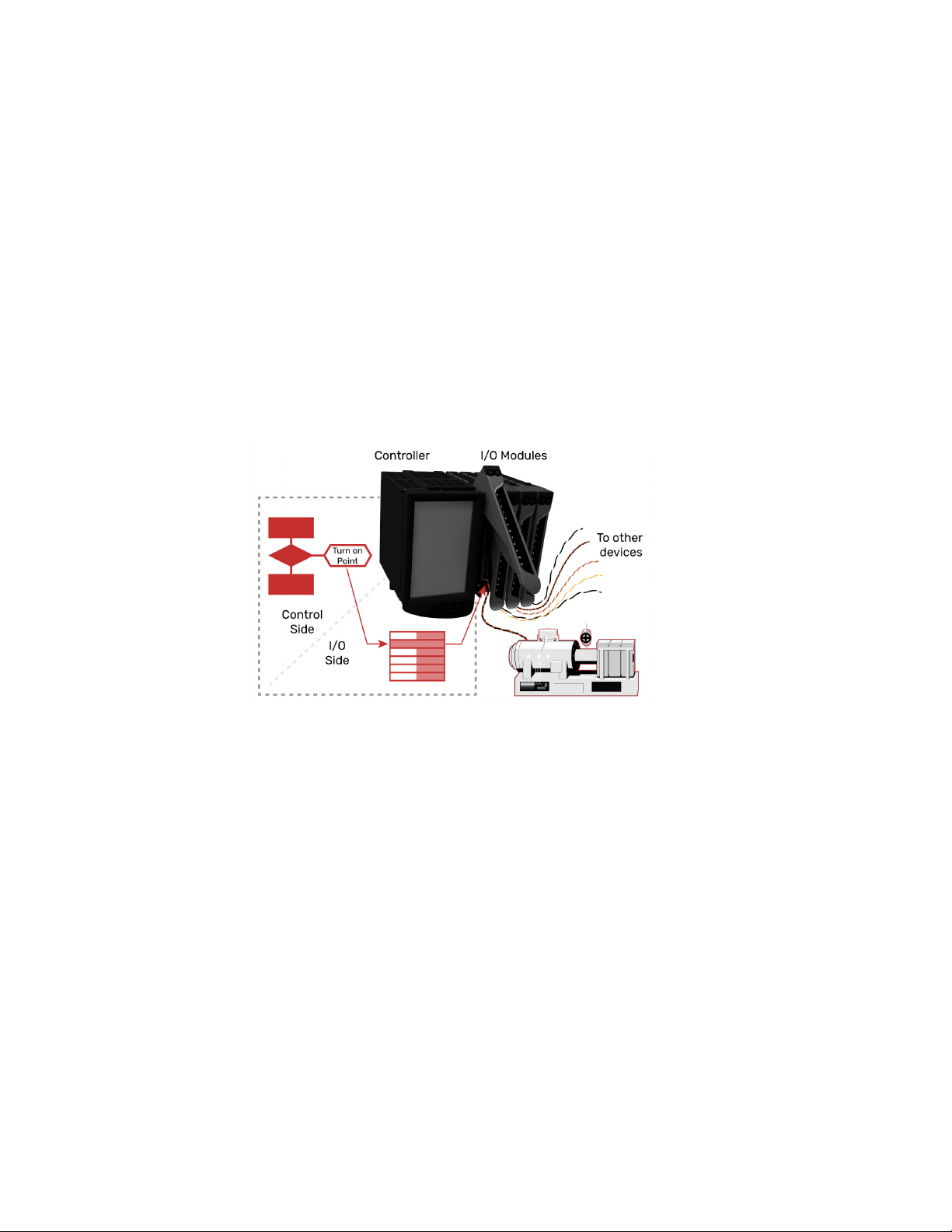
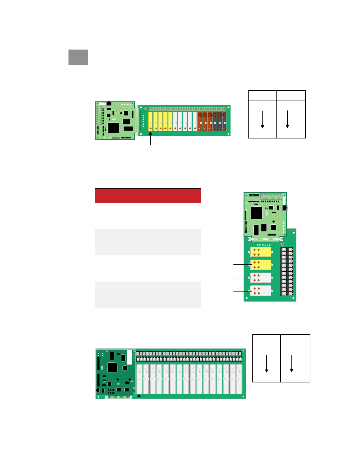
This image depicts a GRV-EPIC-PR1 and
groov I/O modules on a groov EPIC chassis.
Together, these devices are referred to as
an I/O unit.
The modules on the chassis connect with
devices (such as the motor) to monitor
and control them.
Monitoring and control are performed by
sending messages (commands) to
addresses in the groov EPIC processor’s
memory map.
On the control side, these Opto 22 devices have capabilities very much like a SNAP PAC S-series or SNAP-LCE
standalone controller: they typically run a control program developed in PAC Control software. (Some, like
groov EPIC, can run programs developed with other tools.) The control program provides the logic that
controls processes throughout the system. Within the program, PAC Control commands (programming
functions) read and write to the memory map in the I/O side to monitor and control I/O channels.
On the I/O side, these Opto 22 devices have features similar to a SNAP PAC EB brain or a SNAP Ethernet brain:
they read and write to I/O channels by using the memory map (see “Understanding the Memory Map” on
page 8).
IMPORTANT: Any time you are communicating with both the control side and the I/O side, plan carefully and use
caution. The control side reads from and writes to the I/O side just as other methods do directly. Make sure that data
being written directly to the I/O side does not conflict with control logic being executed in the main control program.
OptoMMP Protocol Guide
7
Page 16

UNDERSTANDING THE MEMORY MAP
UNDERSTANDING THE MEMORY MAP
NOTE: Appendix A: Opto 22 Hardware Memory Map shows all memory map addresses and the devices each section
supports.
PR1
RIO
PAC-R
PAC-S
EB
SB
UIO
EIO
SIO
LCE
E1
E2
G4EB2
Opto 22 memory-mapped devices use the IEEE 1394 specification as a standard for reading and writing data.
This standard specifies a memory-mapped model for devices on a network. Basically, each node (such as a
SNAP PAC brain) appears logically as a 48-bit address space2. To communicate with a device, you read from
and write to specific memory addresses in that space.
If you’re a progra mmer, you already know that a memory map is a data structure that matches a set of
logical addresses with physical addresses in the read/write memory hardware on a device. You can think of a
memory map as a lookup table, or if you’re familiar with programmable logic controllers (PLCs), it’s similar to a
PLC’s register.
In Opto 22 memory-mapped devices, a physical address might hold a single value of data, such as the state of
a single digital channel, counter data for a digital channel, the minimum value of an analog channel, or the
device’s firmware version. In your programming code, you use the logical address to reference the physical
address that holds the data you want to read or write to.
When you write to the memory map, the memory-mapped device responds by returning a packet that
indicates success or a failure code. When you perform a read, the memory-mapped device returns a packet
containing the data.
If you’re not a programmer, you can think of a
memory map (sometimes called a mem map) as a
collection of post office boxes. Each mailbox’s address
has a different owner who either has information you
want, or information you want to change.
To get or change the information, you send a message
(in the form of a structured packet of data) to the
mailbox address. For example, to get a device’s part
number, you send the message to address
0080. In response, you’ll get another packet of data
FFFF F030
containing—in this example—the part number.
Getting a part number is an example of reading a
memory map address. You can also write to the
memory map, for example, to change an I/O channel’s
configuration, its status, or its value.
8
OptoMMP Protocol Guide
Note that devices vary in how much of the memory map they support. For example, the SNAP PAC S-series
standalone controller does not support reading or writing to channels, since it is not directly connected to
channels. Similarly, a digital-only brain does not support analog sections of the memory map.
Also note that features included in the memory map may not always be the same as features available
through another protocol. For example, waveform generation is supported on an E2 using the Optomux
protocol, but it is not available on an E2 in OptoMMP. For a list of features supported by each device, see
Appendix C: SNAP Features Comparison Chart and Appendix D: groov EPIC and groov RIO Features and
Comparison Charts.
2
48 bits is equivalent to 6 octets. FFFF F110 0000 is an example of a 48-bit address space.
Page 17

CHAPTER 2: OVERVIEW OF PROGRAMMING
REFERENCING MODULE AND CHANNEL POSITIONS ON I/O UNITS
PR1
RIO
PAC-R
PAC-S
EB
SB
UIO
EIO
SIO
LCE
E1
E2
G4EB2
PR1
NOTE: You can use the reference model described in this section by all methods of communication listed in
“Communication Options” on page 6 except Modbus/TCP and Optomux. For Modbus I/O channel referencing, see
the Modbus chapter in the Modbus/TCP Protocol Guide (form 1678). For Optomux, see the Optomux Protocol
Guide
(form 1572).
Before you begin writing programs that read and write to the memory map addresses in Appendix A: Opto 22
Hardware Memory Map, you first need to know how to reference I/O modules and the channels on them.
Opto 22 I/O units are zero-based: that is, the first module position on the rack or chassis is position 0, and the
first channel on each module is channel 0. The number of channels on a module can vary from one to 32,
depending on the module family and part number. Because of this numbering and variation, it’s important to
understand them before you start reading and writing channel data.
Module and channel positions differ depending on the module family; see the section for yours:
groov I/O Units.................................................................................................. page 9
groov RIO Units...............................................................................................page 10
SNAP I/O Units (and M-series)..................................................................page 11
SNAP B-Series I/O Units............................................................................... page 11
SNAP Digital-Only I/O Units ......................................................................page 12
E1 and E2 I/O Units........................................................................................page 13
G4EB2 I/O Units...............................................................................................page 14
For serial modules, also see page 107.
groov I/O Units
I/O units whose I/O processor is a GRV-EPIC-PR1 are called groov I/O units. groov I/O chassis can hold 4, 8, or 16
I/O modules, and each module contains 8 to 24 channels, depending on the module. Several groov modules
offer a variety of features that you can configure. After you learn how to reference module and channel
positions, then continue to configuring channels and features:
• To configure groov I/O channels, see page 16
• To configure groov I/O features, see page 31.
The following diagram shows examples of groov modules mounted on a chassis, along with the processor.
The diagram also shows examples of how channels are identified on some of the modules.
OptoMMP Protocol Guide
9
Page 18
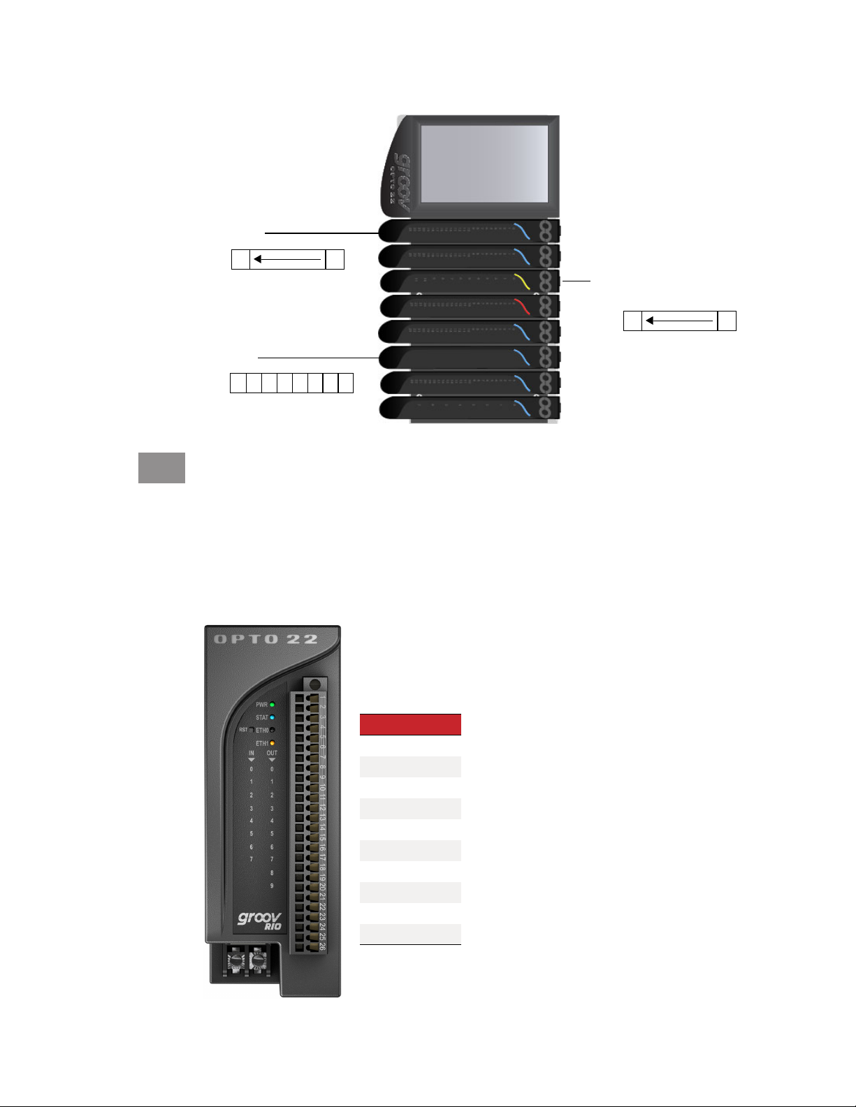
REFERENCING MODULE AND CHANNEL POSITIONS ON I/O UNITS
Module position 0, discrete,
24 channels:
Ch: 23 0
Module position 5, analog,
8 channels:
Ch:76543210
Module position 2, discrete,
12 channels:
Ch: 11 0
RIO
groov RIO Units
A groov RIO module contains an I/O and communications processor plus a specific number of multifunction,
multi-signal I/O channels. Multifunction means channels can be configured as either inputs or outputs;
multi-signal means channels can be configured for different signal inputs. For example, the groov RIO part
number GRV-R7-MM1001-10 includes a processor and ten I/O channels, eight of which are software
configurable as analog or discrete inputs or outputs with a variety of signals, and two of which are Form C
mechanical relays.
All channels on a groov RIO module are considered to be in module position 0. Channel positions are:
GRV-R7-MM1001-10
Channel Positions
Module position = 0
Pins Channel
1–3 0
4–6 1
7–9 2
10–12 3
13–14 4
15–16 5
17–18 6
19–20 7
21–-23 8
24–26 9
To configure channels, see page 20.
To configure channel features, see page 31.
10
OptoMMP Protocol Guide
Page 19
CHAPTER 2: OVERVIEW OF PROGRAMMING
PAC-R
EB
SB
UIO
EIO
SIO
SNAP I/O Units
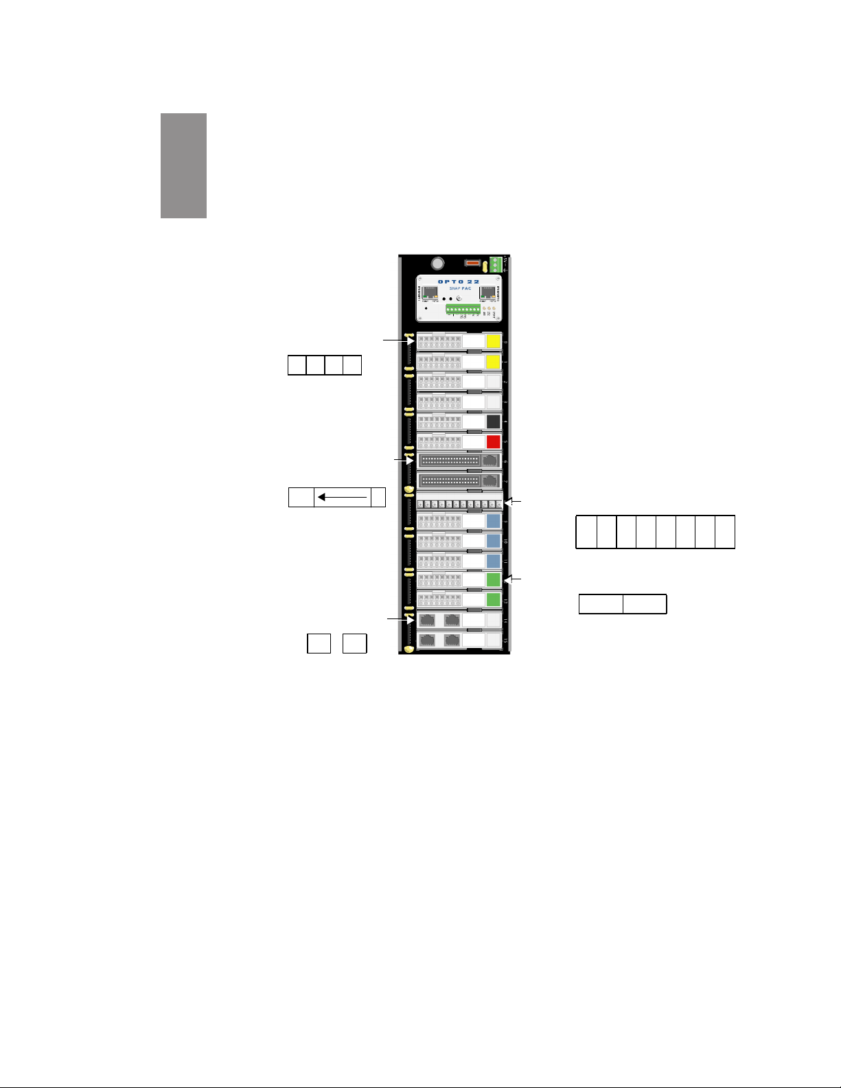
I/O units whose I/O processor’s part number begins with “SNAP” are called SNAP I/O units. For example,
I/O units with a SNAP-PAC-R1, SNAP-EB1, or SNAP-ENET-S64 as the I/O processor are all SNAP I/O units.
SNAP mounting racks may hold 4, 8, 12, or 16 I/O modules, and the modules can be analog, digital, or serial.
Each module contains 1 to 32 channels (points), depending on the module. Examples of modules are shown
in the following diagram.
NOTE: Module support,
functions, and positions vary by
processor.
Module position 0, 4-ch digital:
Channels: 3 2 1 0
Module position 6, high-density
digital:
Channels
:31 0
Module position 8, analog:
Channels
Module position 12, analog:
Channels
Module position 14, serial:
Ports: B A
76543210
:
:1 0
For more information about SNAP I/O channels, see page 21; for SNAP I/O features, see page 31.
SNAP B-Series I/O Units
NOTE: SNAP B-series racks and the processors compatible with them are not recommended for new development.
Use SNAP PAC racks and processors instead.
SNAP B-series mounting racks can hold up to 4, 8, 12, or 16 Opto 22 SNAP I/O modules. (Not all modules are
supported by these processors; for details, see Legacy and Current SNAP Product Comparison and Compatibility
Charts, form 1693.) Analog, serial, and high-density digital modules (digital modules with more than four
channels) can be placed in any position. For the larger racks, 4-channel digital modules can be placed in
positions 0–7 only. Each module contains 1 to 32 channels, depending on the module. Examples of modules
are shown in the following diagram.
OptoMMP Protocol Guide
11
Page 20
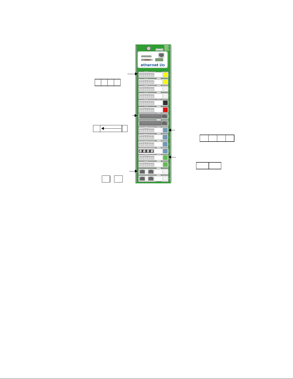
REFERENCING MODULE AND CHANNEL POSITIONS ON I/O UNITS
Module position 0, 4-ch digital:
Channel: 3 2 1 0
Module position 6, high-density
digital:
NOTE: 4-channel digital modules can be
placed in positions 0–7 only.
All other modules can be placed in any
position.
Channels
:31 0
Module position 14, serial:
Ports: B A
Module position 8, analog:
Channels: 3 2 1 0
Module position 12, analog:
Channels: 1 0
SNAP Digital-Only I/O Units
NOTE: Digital-only racks and processors are not recommended for new development. Use SNAP PAC racks and
processors instead.
The SNAP-D64RS mounting rack is compatible with SNAP-UP1-D64 and SNAP-ENET-D64 processors. The rack
holds up to 16 4-channel SNAP digital I/O modules. Analog, serial, and high-density digital modules are not
supported. Module position 0 is the position closest to the processor.
12
OptoMMP Protocol Guide
Page 21
CHAPTER 2: OVERVIEW OF PROGRAMMING
E1
E2
E1 and E2 I/O Units
I/O units using a digital E1 or analog E2 brain board normally use modules containing only one channel, and
the maximum number of channels on the rack is 16. Examples of E1 and E2 I/O units are shown below.
E1 shown with G4 modules.
Since each module has just one channel, use only the first
channel for each module in the memory map.
Module # Channel #
00
15
0
0
Module position 0
E1 with Quad Pak modules.
Quad Pak modules have four input or four output channels, but each
channel is treated as if it were a separate one-channel module.
Module position on
Quad Pak rack
0
1
2
3
Module
number
00
01
02
03
04
05
06
07
08
09
10
11
12
13
14
15
Channel
number
0
0
0
0
0
0
0
0
0
0
0
0
0
0
0
0
0
1
2
3
E2 with G1 modules.
Since each module has just one channel, use only the first
channel for each module in the memory map.
Module position 0
Module # Channel #
00
15
0
0
OptoMMP Protocol Guide
13
Page 22
REFERENCING MODULE AND CHANNEL POSITIONS ON I/O UNITS
G4EB2
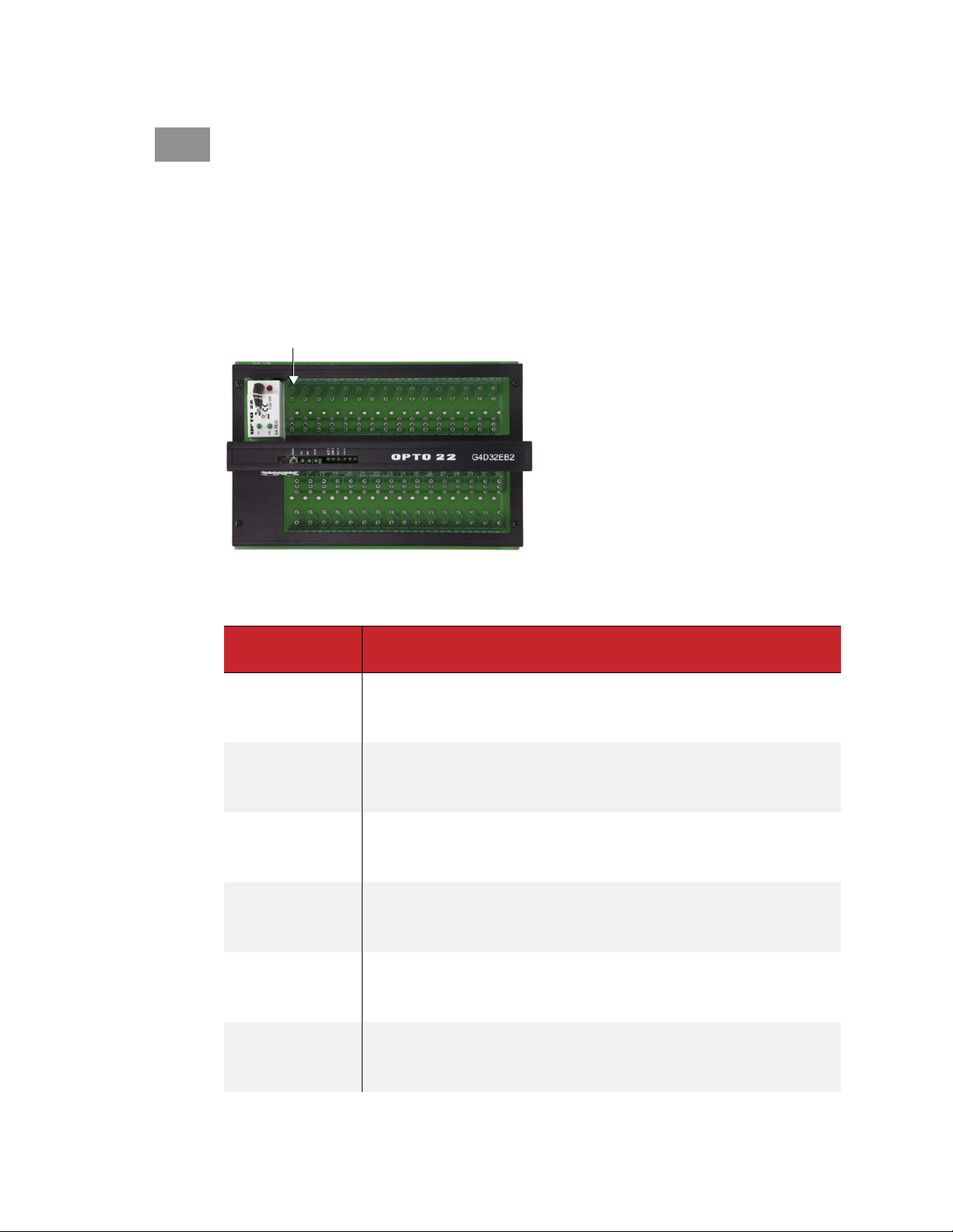
G4EB2 I/O Units
These I/O units include part numbers G4EB2, G4D32EB2, and G4D32EB2-UPG. Each I/O unit has 32 total
channels, all of them digital. They may use G4 modules, which each have one channel, or Quad Pak modules,
which each have four channels of the same type (all four digital inputs or all four digital outputs).
G4EB2 brains with G4 modules
Each module has just one channel (point). However, in the memory map they are addressed like Quad Pak
racks (see page 15). The difference is that with G4s, you can mix input and output modules within the same
group of four channels.
Module position 0
The following table shows Channel Configuration addresses as an example of how to reference channels on a
rack with G4 modules.
G4 rack Memory Map equivalent
Module position Module number Channel number Starting address for channel config
0
1
2
3
4
5
6
7
8
9
10
11
12
13
14
15
16
17
18
19
20
21
22
23
0
0
0
0
1
1
1
1
2
2
2
2
3
3
3
3
4
4
4
4
5
5
5
5
0
1
2
3
0
1
2
3
0
1
2
3
0
1
2
3
0
1
2
3
0
1
2
3
F010 0000
F010 00C0
F010 0180
F010 0240
F010 3000
F010 30C0
F010 3180
F010 3240
F010 6000
F010 60C0
F010 6180
F010 6240
F010 9000
F010 90C0
F010 9180
F010 9240
F010 C000
F010 C0C0
F010 C180
F010 C240
F010 F000
F010 F0C0
F010 F180
F010 F240
14
OptoMMP Protocol Guide
Page 23

CHAPTER 2: OVERVIEW OF PROGRAMMING
G4 rack Memory Map equivalent
Module position Module number Channel number Starting address for channel config
24
25
26
27
28
29
30
31
6
6
6
6
7
7
7
7
0
1
2
3
0
1
2
3
F011 2000
F011 20C0
F011 2180
F011 2240
F011 5000
F011 50C0
F011 5180
F011 5240
G4EB2 brains with Quad Pak modules
Quad Pak modules have four input or four output channels per module, so each group of four channels must
be configured as either inputs or outputs.
Module position 0 (channels 0–3)
The following table shows Channel Configuration addresses as an example of how to reference channels on a
PB32HQ rack with Quad Pak modules.
Quad Pak rack Memory Map equivalent
Module position
0
1
2
3
4
Channel
number
0
1
2
3
4
5
6
7
8
9
10
11
12
13
14
15
16
17
18
19
Module number
0
0
0
0
1
1
1
1
2
2
2
2
3
3
3
3
4
4
4
4
Channel
number
0
1
2
3
0
1
2
3
0
1
2
3
0
1
2
3
0
1
2
3
Starting address for
channel config
F010 0000
F010 00C0
F010 0180
F010 0240
F010 3000
F010 30C0
F010 3180
F010 3240
F010 6000
F010 60C0
F010 6180
F010 6240
F010 9000
F010 90C0
F010 9180
F010 9240
F010 C000
F010 C0C0
F010 C180
F010 C240
OptoMMP Protocol Guide
15
Page 24

CONFIGURING I/O CHANNELS
Quad Pak rack Memory Map equivalent
Module position
5
6
7
CONFIGURING I/O CHANNELS
Before you can read or write to I/O channels, you must make sure channel types and channel features are
configured as required.
Channel
number
20
21
22
23
24
25
26
27
28
29
30
31
Module number
5
5
5
5
6
6
6
6
7
7
7
7
Channel
number
0
1
2
3
0
1
2
3
0
1
2
3
Starting address for
channel config
F010 F000
F010 F0C0
F010 F180
F010 F240
F011 2000
F011 20C0
F011 2180
F011 2240
F011 5000
F011 50C0
F011 5180
F011 5240
PR1
See the section for your I/O unit:
groov I/O units................................................................................................. page 16
groov RIO units................................................................................................ page 20
SNAP analog/digital I/O units.................................................................. page 21
SNAP digital-only and G4EB2 I/O units ............................................... page 29
E1 and E2 brain boards ...............................................................................page 29
Configuring I/O Channels for groov I/O Units
You can configure groov I/O units in three ways:
• PAC Cont rol—If you are programming a strategy with PAC Control (R10.0 or higher), configure channels
while you are programming the strategy.
• groov Mana ge—If your control program is not a PAC Control strategy, configure channels in groov
Manage, either on the groov EPIC processor’s touchscreen or remotely from a computer or mobile device.
Configurations are automatically saved to flash memory.
• OptoMMP—If OptoMMP is the ONLY communication to the groov I/O unit, then configure I/O channels
by selecting the appropriate configuration values as described below.
groov I/O Module Types and Channel Types
The table beginning on page 17 shows configuration values for groov I/O modules, divided by module and
channel types.
• Some modules provide or accept several ranges of values per channel, which is why they have multiple
channel types. If a module offers more than one range, choose the range you want from the Description
column and read across to the Channel ID (hex) column to find the corresponding configuration value.
For example, suppose the module in position (slot) 0 on the chassis is a GRV-IV-24 and you want to
monitor a range of ±10 V on the first two channels (channels 0 and 1). You find the module’s range in the
Description column and read across to see that the appropriate configuration value is 0x60000017.
• Some modules provide or accept only certain configuration values on specific channels. Those modules
list the specific channel that accepts a specific configuration value in the “Applies To” column. If the
16
OptoMMP Protocol Guide
Page 25

CHAPTER 2: OVERVIEW OF PROGRAMMING
column says “all”, that means all channels on that module accept all the configuration values available for
that module.
After you select the configuration value for the module and channel type, go to page 31 to select the correct
configuration value for a specific feature.
Part number
GRV-CSERI-4 all RS232 0C00001E 08000026 4 N/A N/A N/A
GRV-CSERI-4 all RS485, 2-Wire, no termination, no bias 0C00001E 08000027 4 N/A N/A N/A
GRV-CSERI-4 all RS485, 2-Wire, termination, no bias 0C00001E 08000028 4 N/A N/A N/A
GRV-CSERI-4 all RS485, 2-Wire, no termination, bias 0C00001E 08000029 4 N/A N/A N/A
GRV-CSERI-4 all RS485, 2-Wire, termination, bias 0C00001E 0800002A 4 N/A N/A N/A
GRV-CSERI-4 all RS485, 4-Wire, no termination, no bias 0C00001E 0800002B 4 N/A N/A N/A
GRV-CSERI-4 all RS485, 4-Wire, termination, no bias 0C00001E 0800002C 4 N/A N/A N/A
GRV-CSERI-4 all RS485, 4-Wire, no termination, bias 0C00001E 0800002D 4 N/A N/A N/A
GRV-CSERI-4 all RS485, 4-Wire, termination, bias 0C00001E 0800002E 4 N/A N/A N/A
GRV-IAC-24 all Digital Input 5000000F 50000000 24 N/A N/A N/A
GRV-IACDCTTL-24 all Digital Input 50000005 50000000 24 N/A N/A N/A
GRV-IACDCTTLS-24 all Simple Digital Input 54000007 54000000 24 N/A N/A N/A
GRV-IACHV-24 all Digital Input 50000010 50000000 24 N/A N/A N/A
GRV-IACHVS-24 all Simple Digital Input 54000008 54000000 24 N/A N/A N/A
GRV-IACI-12 all Digital Input 5000000C 50000000 12 N/A N/A N/A
GRV-IACIHV-12 all Digital Input 5000000D 50000000 12 N/A N/A N/A
GRV-IACIHVS-12 all Simple Digital Input 54000009 54000000 12 N/A N/A N/A
GRV-IACIS-12 all Simple Digital Input 5400000A 54000000 12 N/A N/A N/A
GRV-IACS-24 all Simple Digital Input 5400001D 54000000 24 N/A N/A N/A
GRV-IDC-24 all Digital Input 50000011 50000000 24 N/A N/A N/A
GRV-IDCI-12 all Digital Input 5000000E 50000000 12 N/A N/A N/A
GRV-IDCIFQ-12 0 Digital Input with Quadrature 5000001A 5000002F 12 N/A N/A N/A
GRV-IDCIFQ-12 1 Digital Input with Quadrature 5000001A 5000002F 12 N/A N/A N/A
GRV-IDCIFQ-12 2 Digital Input with Quadrature Index 5000001A 50000030 12 N/A N/A N/A
GRV-IDCIFQ-12 3 Digital Input with Quadrature 5000001A 5000002F 12 N/A N/A N/A
GRV-IDCIFQ-12 4 Digital Input with Quadrature 5000001A 5000002F 12 N/A N/A N/A
GRV-IDCIFQ-12 5 Digital Input with Quadrature Index 5000001A 50000030 12 N/A N/A N/A
GRV-IDCIFQ-12 6 Digital Input with Quadrature 5000001A 5000002F 12 N/A N/A N/A
GRV-IDCIFQ-12 7 Digital Input with Quadrature 5000001A 5000002F 12 N/A N/A N/A
GRV-IDCIFQ-12 8 Digital Input with Quadrature Index 5000001A 50000030 12 N/A N/A N/A
GRV-IDCIFQ-12 9 Digital Input with Quadrature 5000001A 5000002F 12 N/A N/A N/A
GRV-IDCIFQ-12 10 Digital Input with Quadrature 5000001A 5000002F 12 N/A N/A N/A
GRV-IDCIFQ-12 11 Digital Input with Quadrature Index 5000001A 50000030 12 N/A N/A N/A
GRV-IDCIS-12 all Simple Digital Input 5400000B 54000000 12 N/A N/A N/A
Description
Applies To
(hex)
Module ID
(hex)
Channel ID
Default
Channels
per module
Units
Low Scale
Full Scale
OptoMMP Protocol Guide
17
Page 26

CONFIGURING I/O CHANNELS
Part number
GRV-IDCS-24 all Simple Digital Input 54000016 54000000 24 N/A N/A N/A
GRV-IICTD-12 all ICTD Temperature Probe 6000001F 60000031 12 °C -270 150
GRV-IMA-24 all ±20 mA 60000001 60000014 24 mA -20 20
GRV-IMA-24 all 0-20 mA 60000001 60000015 24 mA 0 20
GRV-IMA-24 all 4-20 mA 60000001 60000016 24 mA 4 20
GRV-IMAI-8 all 0-20 mA 60000020 60000015 8 mA 0 20
GRV-IMAI-8 all 4-20 mA 60000020 60000016 8 mA 4 20
GRV-ITM-12 all ±1200 mV 60000026 60000002 12 mV -1200 1200
GRV-ITM-12 all ±600 mV 60000026 60000003 12 mV -600 600
GRV-ITM-12 all ±300 mV 60000026 60000004 12 mV -300 300
GRV-ITM-12 all ±150 mV 60000026 60000005 12 mV -150 150
GRV-ITM-12 all ±75 mV 60000026 60000006 12 mV -75 75
GRV-ITM-12 all ±50 mV 60000026 60000007 12 mV -50 50
GRV-ITM-12 all ±25 mV 60000026 60000008 12 mV -25 25
GRV-ITM-12 all Type B Thermocouple (°C) 60000026 60000009 12 °C 0 1820
GRV-ITM-12 all Type E Thermocouple (°C) 60000026 6000000C 12 °C -270 1000
GRV-ITM-12 all Type J Thermocouple (°C) 60000026 6000000E 12 °C -210 1200
GRV-ITM-12 all Type K Thermocouple (°C) 60000026 6000000F 12 °C -270 1372
GRV-ITM-12 all Type N Thermocouple (°C) 60000026 60000010 12 °C -270 1300
GRV-ITM-12 all Type R Thermocouple (°C) 60000026 60000011 12 °C -50 1768
GRV-ITM-12 all Type S Thermocouple (°C) 60000026 60000012 12 °C -50 1768
GRV-ITM-12 all Type T Thermocouple (°C) 60000026 60000013 12 °C -270 400
GRV-ITMI-8 all ±1200 mV 60000006 60000002 8 mV -1200 1200
GRV-ITMI-8 all ±600 mV 60000006 60000003 8 mV -600 600
GRV-ITMI-8 all ±300 mV 60000006 60000004 8 mV -300 300
GRV-ITMI-8 all ±150 mV 60000006 60000005 8 mV -150 150
GRV-ITMI-8 all ±75 mV 60000006 60000006 8 mV -75 75
GRV-ITMI-8 all ±50 mV 60000006 60000007 8 mV -50 50
GRV-ITMI-8 all ±25 mV 60000006 60000008 8 mV -25 25
GRV-ITMI-8 all Type B Thermocouple (°C) 60000006 60000009 8 °C 0 1820
GRV-ITMI-8 all Type E Thermocouple (°C) 60000006 6000000C 8 °C -270 1000
GRV-ITMI-8 all Type J Thermocouple (°C) 60000006 6000000E 8 °C -210 1200
GRV-ITMI-8 all Type K Thermocouple (°C) 60000006 6000000F 8 °C -270 1372
GRV-ITMI-8 all Type N Thermocouple (°C) 60000006 60000010 8 °C -270 1300
GRV-ITMI-8 all Type R Thermocouple (°C) 60000006 60000011 8 °C -50 1768
GRV-ITMI-8 all Type S Thermocouple (°C) 60000006 60000012 8 °C -50 1768
GRV-ITMI-8 all Type T Thermocouple (°C) 60000006 60000013 8 °C -270 400
GRV-ITR-12 all Thermistor: 2252 Curve (°C) 60000021 6000003F 12 °C -40 150
GRV-ITR-12 all Thermistor: 3K Curve (°C) 60000021 60000040 12 °C -40 150
Description
Applies To
(hex)
Module ID
(hex)
Channel ID
Default
Channels
per module
Units
Low Scale
Full Scale
18
OptoMMP Protocol Guide
Page 27

CHAPTER 2: OVERVIEW OF PROGRAMMING
Part number
GRV-ITR-12 all Thermistor: 10K Type 2 Curve (°C) 60000021 60000041 12 °C -40 150
GRV-ITR-12 all Thermistor: 10K Type 3 Curve (°C) 60000021 60000042 12 °C -40 150
GRV-ITR-12 all Thermistor: Custom Curve (°C) 60000021 60000043 12 °C -40 150
GRV-ITR-12 all 0–400k Ohms (autorange) 60000021 60000032 12 Ohms 0 400000
GRV-ITR-12 all 0–400k Ohms 60000021 60000033 12 Ohms 0 400000
GRV-ITR-12 all 0–200k Ohms 60000021 60000034 12 Ohms 0 200000
GRV-ITR-12 all 0–100k Ohms 60000021 60000035 12 Ohms 0 100000
GRV-ITR-12 all 0–50k Ohms 60000021 60000036 12 Ohms 0 50000
GRV-ITR-12 all 0–40k Ohms 60000021 60000037 12 Ohms 0 40000
GRV-ITR-12 all 0–20k Ohms 60000021 60000038 12 Ohms 0 20000
GRV-ITR-12 all 0–10k Ohms 60000021 60000039 12 Ohms 0 10000
GRV-ITR-12 all 0–5k Ohms 60000021 6000003A 12 Ohms 0 5000
GRV-ITR-12 all 0–4k Ohms 60000021 6000003B 12 Ohms 0 4000
GRV-ITR-12 all 0–2k Ohms 60000021 6000003C 12 Ohms 0 2000
GRV-ITR-12 all 0–1k Ohms 60000021 6000003D 12 Ohms 0 1000
GRV-ITR-12 all 0–500 Ohms 60000021 6000003E 12 Ohms 0 500
GRV-IV-24 all ±160 V 60000002 60000024 24 V -160 160
GRV-IV-24 all ±80 V 60000002 6000000D 24 V -80 80
GRV-IV-24 all ±40 V 60000002 6000000B 24 V -40 40
GRV-IV-24 all ±20 V 60000002 6000000A 24 V -20 20
GRV-IV-24 all ±10 V 60000002 60000017 24 V -10 10
GRV-IV-24 all ±5 V 60000002 60000019 24 V -5 5
GRV-IV-24 all ±2.5 V 60000002 60000025 24 V -2.5 2.5
GRV-IV-24 all ±1.25 V 60000002 60000001 24 V -1.25 1.25
GRV-OAC-12 all Digital Output 90000012 90000000 12 N/A N/A N/A
GRV-OACI-12 all Digital Output 90000014 90000000 12 N/A N/A N/A
GRV-OACIS-12 all Simple Digital Output 94000017 94000000 12 N/A N/A N/A
GRV-OACS-12 all Simple Digital Output 9400001C 94000000 12 N/A N/A N/A
GRV-ODCI-12 all Digital Output 90000015 90000000 12 N/A N/A N/A
GRV-ODCIS-12 all Simple Digital Output 94000018 94000000 12 N/A N/A N/A
GRV-ODCSRC-24 all Digital Output 90000013 90000000 24 N/A N/A N/A
GRV-OMRIS-8 all Simple Digital Output 94000019 94000000 8 N/A N/A N/A
GRV-OVMAILP-8 all 0-20 mA A0000004 A000001B 8 mA 0 20
GRV-OVMAILP-8 all 0-24 mA A0000004 A000001C 8 mA 0 24
GRV-OVMAILP-8 all 4-20 mA A0000004 A000001D 8 mA 4 20
GRV-OVMAILP-8 all 0-10 V A0000004 A0000020 8 V 0 10
GRV-OVMAILP-8 all 0-5 V A0000004 A0000022 8 V 0 5
GRV-OVMAILP-8 all Analog Hi-Z A0000004 A0000023 8 None 0 0
GRV-OVMALC-8 all 0-20 mA A0000003 A000001B 8 mA 0 20
Description
Applies To
(hex)
Module ID
(hex)
Channel ID
Default
Channels
per module
Units
Low Scale
Full Scale
OptoMMP Protocol Guide
19
Page 28

CONFIGURING I/O CHANNELS
Part number
GRV-OVMALC-8 all 0-24 mA A0000003 A000001C 8 mA 0 24
GRV-OVMALC-8 all 4-20 mA A0000003 A000001D 8 mA 4 20
GRV-OVMALC-8 all ±10 V A0000003 A000001F 8 V -10 10
GRV-OVMALC-8 all 0-10 V A0000003 A0000020 8 V 0 10
GRV-OVMALC-8 all ±5 V A0000003 A0000021 8 V -5 5
GRV-OVMALC-8 all 0-5 V A0000003 A0000022 8 V 0 5
GRV-OVMALC-8 all Analog Hi-Z A0000003 A0000023 8 None 0 0
Description
Applies To
(hex)
Module ID
(hex)
Channel ID
Default
Channels
per module
Units
Low Scale
Configuring I/O Channels for groov RIO Units
You can configure groov RIO units in three ways:
• PAC Control—If you are using PAC Control to create a strategy for your groov EPIC or SNAP PAC
controller, configure channels there while you are programming your strategy.
• groov Manage—If your control program is not a PAC Control strategy, or if you are not using a control
program, configure channels in groov Manage using a web browser on a computer or mobile device.
Configurations are automatically saved to flash memory.
• OptoMMP—If OptoMMP is the ONLY communication to the groov RIO unit, then configure I/O channels
using the configuration values in the following table.
All channels on a groov RIO unit use module ID 0xF0000022.
Full Scale
To configure each channel, use the following channel IDs. Make sure the channel you’re configuring can use
the signal you want.
IMPORTANT: Thermocouple inputs and discrete sinking outputs cannot be mixed on channels 0–3.
To achieve the best thermocouple accuracy when also using current outputs or discrete outputs, always configure
thermocouples on the lowest channel numbers and outputs on the highest channel numbers.
Channels Function Signal
0–1
2–7
0–1
2–7
0–7 Discrete DC output, sinking 5–30 VDC 9000007B VDC 5 30 30
0–7 Analog voltage input 0-10 VDC 60000018 VDC 0 10 11.1
0–7 ICTD (with ICTD probe) -40 to 100 °C 60000031 Degrees C -40 100 100
0–3 Analog current input 0–20 mA 60000015 mA 0 20 22.2
0–3 Thermocouple input Type B 60000009 mV -75 75 -78 to +78
0–3 Thermocouple input Type E 6000000C mV -75 75 -78 to +78
0–3 Thermocouple input Type J 6000000E mV -75 75 -78 to +78
Discrete DC input with
features (see page 169)
Simple discrete DC input
(on/off state only)
Discrete switch input with
features (see page 169)
Simple discrete switch input
(on/off state only)
5–30 VDC 50000079 VDC 5 30 30
5–30 VDC 5400007A VDC 5 30 30
Switch input, powered 50000068 n/a n/a n/a n/a
Switch input, powered 54000085 n/a n/a n/a n/a
Channel ID
(hex)
Default units
Low
Scale
Full
Scale
Overrange
20
OptoMMP Protocol Guide
Page 29

CHAPTER 2: OVERVIEW OF PROGRAMMING
Channels Function Signal
0–3 Thermocouple input Type K 6000000F mV -75 75 -78 to +78
0–3 Thermocouple input Type N 60000010 mV -75 75 -78 to +78
0–3 Thermocouple input Type R 60000011 mV -75 75 -78 to +78
0–3 Thermocouple input Type S 60000012 mV -75 75 -78 to +78
0–3 Thermocouple input Type T 60000013 mV -75 75 -78 to +78
0–3 Analog millivolt input -150 to +150 mV 60000005 mV -150 150 166.5
0–3 Analog millivolt input -75 to +75 mV 60000006 mV -75 75 83.25
0–3 Analog millivolt input -25 to +25 mV 60000008 mV -25 25 27.75
4–7 Analog voltage output 0 to 10 V A0000020 V 0 10 10
4–7 Analog current output 0 to 20 mA A000001B mA 0 20 20
8–9 Mechanical relayoutput Form C 94000078 n/a n/a n/a n/a
Channel ID
(hex)
Default units
Low
Scale
Full
Scale
Overrange
Configuring I/O Channels for SNAP Analog/Digital I/O Units
All SNAP analog/digital I/O units recognize analog, serial, and high-density digital modules on the rack.
Positions on the rack that don’t contain modules the I/O unit recognizes are assumed to contain digital input
modules. If the individual channel types on the module differ from the default type for that module, you must
configure the channels.
You can configure SNAP I/O units in three ways:
• PAC Control—If you are using PAC Control, configure channels there while you are programming your
strategy.
• PAC Manager—If you are not using PAC Control, configure channels in PAC Manager and save to flash
memory.
CAUTION: Store to flash only once! Storing to flash memory in a loop can wear out the memory.
• OptoMMP —If OptoMMP is the ONLY communication to the SNAP I/O unit, then use the values in the
SNAP I/O module types and channel types tables (starting on page 21) to configure I/O channels. For
SNAP digital-only I/O units, G4EB2s, and E1 and E2 brain boards, see page 29.
About E1 and E2 brain boards: You can configure E1s and E2s like any other I/O unit if you have E1/E2 firmware R1.2a
(and higher) and PAC Project 9.5000 (and higher). Also, if a SNAP PAC controller communicates with the E1 or E2, the
controller must have PAC firmware R9.5a (or higher) to use this simplified configuration method. If you are not using
these firmware and software versions (or if you prefer to use the previous method to reconfigure existing E1s or E2s),
see I/O Configuration for E1 an E2 Brain Boards (form 1576).
SNAP I/O Module Types and Channel Types
The following tables help you configure channels by showing the part number, the channel type in decimal
and in hex, and the module type in hex (module type is read-only). For analog modules, tables also include
the number of channels per module, the unit of measurement for the module, and its range. (Some older I/O
units cannot use all of these modules; see the module’s data sheet for compatibility.)
Default channel types are shaded. If a channel differs from the default, use the value in the Channel Type (Hex)
column to configure the channel. For example, if the module in position 0 on the rack is a SNAP-AIV with a -5
to +5 V input, it is not the default for that module. Therefore, you must configure its channels.
As another example, suppose the module in position 1 on the rack is a 4-channel digital output module. Since
the default is a 4-channel digital input module, you must configure its channels.
OptoMMP Protocol Guide
21
Page 30

CONFIGURING I/O CHANNELS
In This Section
SNAP Digital Inputs and Outputs............................................................... Below
SNAP Analog Inputs..................................................................................... page 22
SNAP Analog Outputs ................................................................................. page 28
Digital-only SNAP and G4EB2 I/O units............................................... page 29
E1 and E2 brain boards. ..............................................................................page 29
SNAP Digital Inputs and Outputs
Module & Description
4-channel digital input module* 256 100 00
4-channel digital output module* 384 180 00
* High-density digital modules are automatically recognized; channels do not require configuration.
Channel Type
(Dec)
Channel Type
(Hex)
Module Type (Hex)
SNAP Analog Inputs
Use this data for configuring channel types (see page 21) and features (see page 31).
If a module has multiple listings, the default channel type is shaded.
Part Number &
Description
Measurement
Channel Type (Dec)
SNAP-AIARMS: 0–10 A AC/DC 71 47 71 2 A 0.0 0.0 10.0 11.0
SNAP-AIARMS-i: 0–10 A AC/DC 71 47 29 2 A 0.0 0.0 10.0 11.0
SNAP-AIARMS-i-FM: 0–10 A AC/DC 71 47 29 2 A 0.0 0.0 10.0 11.0
SNAP-AICTD: ICTD Temp. Probe 4 4 04 2 Degrees C -273.0 -40.0 150.0 150.0
SNAP-AICTD-4: ICTD Temp. Probe 4 4 42 4 Degrees C -273.0 -40.0 150.0 150.0
SNAP-AICTD-8: ICTD Temp. Probe 4 4 4C 8 Degrees C -273.0 -40.0 150.0 150.0
SNAP-AILC: -2 to +2 mV/V Fast 34 22 0B 2 Percent -110.0 -100.0 100.0 110.0
SNAP-AILC: -2 to +2 mV/V Slow 36 24 0B 2 Percent -110.0 -100.0 100.0 110.0
SNAP-AILC: -3 to +3 mV/V Fast 35 23 0B 2 Percent -110.0 -100.0 100.0 110.0
SNAP-AILC: -3 to +3 mV/V Slow 37 25 0B 2 Percent -110.0 -100.0 100.0 110.0
SNAP-AILC: Filter of 1st channel 0 0 0B 2 Percent -110.0 -100.0 100.0 110.0
SNAP-AILC-2: -3 to +3 mV/V Fast 35 23 0C 2 Percent -110.0 -100.0 100.0 110.0
SNAP-AILC-2: -3 to +3 mV/V Slow 37 25 0C 2 Percent -110.0 -100.0 100.0 110.0
SNAP-AILC-2: -4 to +4 mV/V Fast 34 22 0C 2 Percent -110.0 -100.0 100.0 110.0
SNAP-AILC-2: -4 to +4 mV/V Slow 36 24 0C 2 Percent -110.0 -100.0 100.0 110.0
SNAP-AILC-2: Filter of 1st channel 0 0 0C 2 Percent -110.0 -100.0 100.0 110.0
SNAP-AIMA: -20 to +20 mA 64 40 64 2 mA -22.0 -20.0 20.0 22.0
SNAP-AIMA: 0 to +20 mA 2 2 64 2 mA -22.0 0.0 20.0 22.0
SNAP-AIMA: 4 to +20 mA 3 3 64 2 mA -22.0 4.0 20.0 22.0
SNAP-AIMA2-i: -1 to +1 mA 85 55 27 2 mA -1.1 -1.0 1.0 1.1
Module Type (Hex)
Channel Type (Hex)
Default Unit of
Channels per Module
Underrange
Low Scale
Full Scale
Overrange
22
OptoMMP Protocol Guide
Page 31

CHAPTER 2: OVERVIEW OF PROGRAMMING
Part Number &
Description
Measurement
Channel Type (Dec)
SNAP-AIMA-i: -20 to +20 mA 64 40 22 2 mA -22.0 -20.0 20.0 22.0
SNAP-AIMA-i: 0 to +20 mA 2 2 22 2 mA -22.0 0.0 20.0 22.0
SNAP-AIMA-i: 4 to +20 mA 3 3 22 2 mA -22.0 4.0 20.0 22.0
SNAP-AIMA-iH: 4 to +20 mA 3 3 2A 2 mA 3.2 4.0 20.0 24.0
SNAP-AIMA-iSRC: -20 to +20 mA 64 40 26 2 mA -22.0 -20.0 20.0 22.0
SNAP-AIMA-iSRC: 0 to +20 mA 2 2 26 2 mA -22.0 0.0 20.0 22.0
SNAP-AIMA-iSRC: 4 to +20 mA 3 3 26 2 mA -22.0 4.0 20.0 22.0
SNAP-AIMA-iSRC-FM: -20 to +20 mA 64 40 26 2 mA -22.0 -20.0 20.0 22.0
SNAP-AIMA-iSRC-FM: 0 to +20 mA 2 2 26 2 mA -22.0 0.0 20.0 22.0
SNAP-AIMA-iSRC-FM: 4 to +20 mA 3 3 26 2 mA -22.0 4.0 20.0 22.0
SNAP-AIMA-4: -20 to +20 mA 64 40 40 4 mA -22.0 -20.0 20.0 22.0
SNAP-AIMA-4: 0 to +20 mA 2 2 40 4 mA -22.0 0.0 20.0 22.0
SNAP-AIMA-4: 4 to +20 mA 3 3 40 4 mA -22.0 4.0 20.0 22.0
SNAP-AIMA-8: -20 to +20 mA 64 40 4A 8 mA -22.0 -20.0 20.0 22.0
SNAP-AIMA-8: 0 to +20 mA 2 2 4A 8 mA -22.0 0.0 20.0 22.0
SNAP-AIMA-8: 4 to +20 mA 3 3 4A 8 mA -22.0 4.0 20.0 22.0
SNAP-AIMA-32: -20 to +20 mA 64 40 4D 32 mA -22.0 -20.0 20.0 22.0
SNAP-AIMA-32: 0 to +20 mA 2 2 4D 32 mA -22.0 0.0 20.0 22.0
SNAP-AIMA-32: 4 to +20 mA 3 3 4D 32 mA -22.0 4.0 20.0 22.0
SNAP-AIMA-32-FM: -20 to +20 mA 64 40 4D 32 mA -22.0 -20.0 20.0 22.0
SNAP-AIMA-32-FM: 0 to +20 mA 2 2 4D 32 mA -22.0 0.0 20.0 22.0
SNAP-AIMA-32-FM: 4 to +20 mA 3 3 4D 32 mA -22.0 4.0 20.0 22.0
SNAP-AIMV-4: -150 to +150 mV 66 42 44 4 mV -165.0 -150.0 150.0 165.0
SNAP-AIMV-4: -75 to +75 mV 68 44 44 4 mV -82.5 -75.0 75.0 82.5
SNAP-AIMV2-4: -50 to +50 mV 9 9 45 4 mV -55.0 -50.0 50.0 55.0
SNAP-AIMV2-4: -25 to +25 mV 67 43 45 4 mV -27.5 -25.0 25.0 27.5
SNAP-AIPM (channel 0 only) 70 46 0A *
SNAP-AIPM (channel 1 only) 71 47 0A *
SNAP-AIPM (channel 2 only) 82 52 0A *
SNAP-AIPM (channel 3 only) 83 53 0A *
SNAP-AIPM-3 (channels 0, 4 & 8) 70 46 49 *
SNAP-AIPM-3 (channels 1, 5 & 9) 71 47 49 *
SNAP-AIPM-3 (channels 2, 6 & 10) 82 52 49 *
SNAP-AIPM-3 (channels 3, 7 & 11) 83 53 49 *
SNAP-AIPM-3 (channels 12 & 13) 86 56 49 *
SNAP-AIPM-3V (channels 0, 4 & 8) 100 64 48 *
Module Type (Hex)
Channel Type (Hex)
Default Unit of
Channels per Module
AC VRMS
AC ARMS
True power
Volt/Amps
AC VRMS
AC ARMS
True power
Volt/Amps
True power
AC VRMS
Underrange
0.0 0 250 275
0.0 0 10 11.0
n/a n/a n/a n/a
n/a n/a n/a n/a
0.0 0 300 330
0.0 0 5 5.5
n/a n/a n/a n/a
n/a n/a n/a n/a
n/a n/a n/a n/a
0.0 0 300 330
Low Scale
Full Scale
Overrange
OptoMMP Protocol Guide
23
Page 32

CONFIGURING I/O CHANNELS
SNAP-AIPM-3V (channels 1, 5 & 9) 89 59 48 *
SNAP-AIPM-3V (channels 2, 6 & 10) 90 5A 48 *
SNAP-AIPM-3V (channels 3, 7 & 11) 90 5A 48 *
SNAP-AIPM-3V (channels 12 & 13) 184 B8 48 *
SNAP-AIRATE: Rate (Frequency) 69 45 69 2 Hz 0.0 0.0
SNAP-AIRATE-HFi: Rate (0.1 s data
freshness)
SNAP-AIRATE-HFi: Rate (1 s data
freshness)
SNAP-AIRTD: 100 Ohm Pt 3-wire 10 0A 10 2 Degrees C -200.0 -200.0 850.0 850.0
SNAP-AIRTD: 100 Ohm Ni 3-wire 46 2E 10 2 Degrees C -60.0 -60.0 250.0 250.0
SNAP-AIRTD: 0–400 Ohms, Lead
Compensated
SNAP-AIRTD: 120 Ohm Ni 3-wire 48 30 10 2 Degrees C -80.0 -80.0 260.0 260.0
SNAP-AIRTD-10: 10 Ohm Cu 3-wire 14 0E 0E 2 Degrees C -180.0 -180.0 260.0 260.0
SNAP-AIRTD-10: 0–25 Ohms, Lead
Compensated
SNAP-AIRTD-1K: 1000 Ohm Pt 3-wire 92 5C 0F 2 Degrees C -200.0 -200.0 850.0 850.0
SNAP-AIRTD-1K: 1000 Ohm Ni 3-wire 93 5D 0F 2 Degrees C -60.0 -60.0 250.0 250.0
SNAP-AIRTD-1K: 1000 Ohm Ni 3-wire 94 5E 0F 2 Degrees F -50.0 -50.0 275.0 275.0
SNAP-AIRTD-1K: 0–4000 Ohms, Lead
Compensated
SNAP-AIRTD-8U: 0–8000 Ohms - Fixed 155 9B 55 8 Ohms 0 0 8000 8800
SNAP-AIRTD-8U: 1000 Ohm Ni 3-wire @
70° F
SNAP-AIRTD-8U: 1000 Ohm Ni 3-wire @
0 °C
SNAP-AIRTD-8U: 1000 Ohm Pt @ 0 °C 180 B4 55 8 Degrees C -200 -200 850 850
SNAP-AIRTD-8U: 120 Ohm Ni @ 0 °C 179 B3 55 8 Degrees C -80 -80 260 260
SNAP-AIRTD-8U: 100 Ohm Ni @ 0 °C 178 B2 55 8 Degrees C -60 -60 250 250
SNAP-AIRTD-8U: 100 Ohm Pt @ 0 °C 177 B1 55 8 Degrees C -200 -200 850 850
SNAP-AIRTD-8U: 10 Ohm Cu 176 B0 55 8 Degrees C -60 -60 355 355
SNAP-AIRTD-8U: 0–8000 Ohms - Auto 171 AB 55 8 Ohms 0 0 8000 8800
SNAP-AIRTD-8U: 0–4000 Ohms - Auto 170 AA 55 8 Ohms 0 0 4000 4400
SNAP-AIRTD-8U: 0–2000 Ohms - Auto 169 A9 55 8 Ohms 0 0 2000 2200
SNAP-AIRTD-8U: 0–1000 Ohms - Auto 168 A8 55 8 Ohms 0 0 1000 1100
SNAP-AIRTD-8U: 0–800 Ohms - Auto 167 A7 55 8 Ohms 0 0 800 880
SNAP-AIRTD-8U: 0–400 Ohms - Auto 166 A6 55 8 Ohms 0 0 400 440
SNAP-AIRTD-8U: 0–200 Ohms - Auto 165 A5 55 8 Ohms 0 0 200 220
Part Number &
Description
Measurement
Channel Type (Dec)
68 44 2B 2 Hz 2 2
69 45 2B 2 Hz 20 20
15 0F 10 2 Ohms 0 0 400 440
15 0F 0E 2 Ohms 0 0 25 27.5
15 0F 0F 2 Ohms 0 0 4000 4400
182 B6 55 8 Degrees F -46 -46 148.9 148.9
181 B5 55 8 Degrees C -40 -40 135 135
Module Type (Hex)
Channel Type (Hex)
Default Unit of
Channels per Module
VAC from CT
True power
Volt/Amps
True power
Underrange
0.0 0 0.333 0.366
n/a n/a n/a n/a
n/a n/a n/a n/a
n/a n/a n/a n/a
Low Scale
Full Scale
25000.0 27500.0
500,000 500,000
500,000 500,000
Overrange
24
OptoMMP Protocol Guide
Page 33

CHAPTER 2: OVERVIEW OF PROGRAMMING
Part Number &
Description
Measurement
Channel Type (Dec)
SNAP-AIRTD-8U: 0–100 Ohms - Auto 164 A4 55 8 Ohms 0 0 100 110
SNAP-AIRTD-8U: 0–80 Ohms - Auto 163 A3 55 8 Ohms 0 0 80 88
SNAP-AIRTD-8U: 0–40 Ohms - Auto 162 A2 55 8 Ohms 0 0 40 44
SNAP-AIRTD-8U: 0–20 Ohms - Auto 161 A1 55 8 Ohms 0 0 20 22
SNAP-AIRTD-8U: 0–10 Ohms - Auto 160 A0 55 8 Ohms 0 0 10 11
SNAP-AIRTD-8U: 0–4000 Ohms - Fixed 154 9A 55 8 Ohms 0 0 4000 4400
SNAP-AIRTD-8U: 0–2000 Ohms - Fixed 153 99 55 8 Ohms 0 0 2000 2200
SNAP-AIRTD-8U: 0–1000 Ohms - Fixed 152 98 55 8 Ohms 0 0 1000 1100
SNAP-AIRTD-8U: 0–800 Ohms - Fixed 151 97 55 8 Ohms 0 0 800 880
SNAP-AIRTD-8U: 0–400 Ohms - Fixed 150 96 55 8 Ohms 0 0 400 440
SNAP-AIRTD-8U: 0–200 Ohms - Fixed 149 95 55 8 Ohms 0 0 200 220
SNAP-AIRTD-8U: 0–100 Ohms - Fixed 148 94 55 8 Ohms 0 0 100 110
SNAP-AIRTD-8U: 0–80 Ohms - Fixed 147 93 55 8 Ohms 0 0 80 88
SNAP-AIRTD-8U: 0–40 Ohms - Fixed 146 92 55 8 Ohms 0 0 40 44
SNAP-AIRTD-8U: 0–20 Ohms - Fixed 145 91 55 8 Ohms 0 0 20 22
SNAP-AIRTD-8U: 0–10 Ohms - Fixed 144 90 55 8 Ohms 0 0 10 11
SNAP-AITM: -150 to +150 mV 66 42 66 2 mV -165.0 -150.0 150.0 165.0
SNAP-AITM: -75 to +75 mV 68 44 66 2 mV -82.5 -75.0 75.0 82.5
SNAP-AITM: Type E Thermocouple 19 13 66 2 Degrees C -270.0 -270.0 1000.0 1000.0
SNAP-AITM: Type J Thermocouple 5 5 66 2 Degrees C -210.0 -210.0 1200.0 1200.0
SNAP-AITM: Type K Thermocouple 8 8 66 2 Degrees C -270.0 -270.0 1372.0 1372.0
SNAP-AITM-i: -150 to +150 mV 66 42 20 2 mV -165.0 -150.0 150.0 165.0
SNAP-AITM-i: -75 to +75 mV 68 44 20 2 mV -82.5 -75.0 75.0 82.5
SNAP-AITM-i: Type E Thermocouple 19 13 20 2 Degrees C -270.0 -270.0 1000.0 1000.0
SNAP-AITM-i: Type J Thermocouple 5 5 20 2 Degrees C -210.0 -210.0 1200.0 1200.0
SNAP-AITM-i: Type K Thermocouple 8 8 20 2 Degrees C -270.0 -270.0 1372.0 1372.0
SNAP-AITM-4i: -150 to +150 mV 66 42 32 4 mV -165.0 -150.0 150.0 165.0
SNAP-AITM-4i: -75 to +75 mV 68 44 32 4 mV -82.5 -75.0 75 82.5
SNAP-AITM-4i: -50 to +50 mV 9 9 32 4 mV -55.0 -50.0 50.0 55.0
SNAP-AITM-4i: -25 to +25 mV 67 43 32 4 mV -27.5 -25.0 25.0 27.5
SNAP-AITM-4i: Type B Thermocouple 24 18 32 4 Degrees C 42.0 42.0 1820.0 1820.0
SNAP-AITM-4i: Type C Thermocouple 32 20 32 4 Degrees C 0.0 0.0 2320.0 2320.0
SNAP-AITM-4i: Type D Thermocouple 33 21 32 4 Degrees C 0.0 0.0 2320.0 2320.0
SNAP-AITM-4i: Type E Thermocouple 19 13 32 4 Degrees C -270.0 -270.0 1000.0 1000.0
SNAP-AITM-4i: Type G Thermocouple 31 1F 32 4 Degrees C 0.0 0.0 2320.0 2320.0
SNAP-AITM-4i: Type J Thermocouple 5 5 32 4 Degrees C -210.0 -210.0 1200.0 1200.0
Module Type (Hex)
Channel Type (Hex)
Default Unit of
Channels per Module
Underrange
Low Scale
Full Scale
Overrange
OptoMMP Protocol Guide
25
Page 34

CONFIGURING I/O CHANNELS
SNAP-AITM-4i: Type K Thermocouple 8 8 32 4 Degrees C -270.0 -270.0 1372.0 1372.0
SNAP-AITM-4i: Type N Thermocouple 30 1E 32 4 Degrees C -270.0 -270.0 1300.0 1300.0
SNAP-AITM-4i: Type R Thermocouple 17 11 32 4 Degrees C -50.0 -50.0 1768.0 1768.0
SNAP-AITM-4i: Type S Thermocouple 23 17 32 4 Degrees C -50.0 -50.0 1768.0 1768.0
SNAP-AITM-4i: Type T Thermocouple 18 12 32 4 Degrees C -270.0 -270.0 400.0 400.0
SNAP-AITM-8: -75 to +75 mV 68 44 4F 8 mV -82.5 -75.0 75.0 82.5
SNAP-AITM-8: -50 to +50 mV 9 9 4F 8 mV -55.0 -50.0 50.0 55.0
SNAP-AITM-8: -25 to +25 mV 67 43 4F 8 mV -27.5 -25.0 25.0 27.5
SNAP-AITM-8: Type B Thermocouple 24 18 4F 8 Degrees C 42.0 42.0 1820.0 1820.0
SNAP-AITM-8: Type C Thermocouple 32 20 4F 8 Degrees C 0.0 0.0 2320.0 2320.0
SNAP-AITM-8: Type D Thermocouple 33 21 4F 8 Degrees C 0.0 0.0 2320.0 2320.0
SNAP-AITM-8: Type E Thermocouple 19 13 4F 8 Degrees C -270.0 -270.0 1000.0 1000.0
SNAP-AITM-8: Type G Thermocouple 31 1F 4F 8 Degrees C 0.0 0.0 2320.0 2320.0
SNAP-AITM-8: Type J Thermocouple 5 5 4F 8 Degrees C -210.0 -210.0 1200.0 1200.0
SNAP-AITM-8: Type K Thermocouple 8 8 4F 8 Degrees C -270.0 -270.0 1372.0 1372.0
SNAP-AITM-8: Type N Thermocouple 30 1E 4F 8 Degrees C -270.0 -270.0 1300.0 1300.0
SNAP-AITM-8: Type R Thermocouple 17 11 4F 8 Degrees C -50.0 -50.0 1768.0 1768.0
SNAP-AITM-8: Type S Thermocouple 23 17 4F 8 Degrees C -50.0 -50.0 1768.0 1768.0
SNAP-AITM-8: Type T Thermocouple 18 12 4F 8 Degrees C -270.0 -270.0 400.0 400.0
SNAP-AITM-8-FM: -75 to +75 mV 68 44 4F 8 mV -82.5 -75.0 75.0 82.5
SNAP-AITM-8-FM: -50 to +50 mV 9 9 4F 8 mV -55.0 -50.0 50.0 55.0
SNAP-AITM-8-FM: -25 to +25 mV 67 43 4F 8 mV -27.5 -25.0 25.0 27.5
SNAP-AITM-8-FM: Type B Thermocouple
SNAP-AITM-8-FM: Type C Thermocouple
SNAP-AITM-8-FM: Type D Thermocouple
SNAP-AITM-8-FM: Type E Thermocouple
SNAP-AITM-8-FM: Type G Thermocouple
SNAP-AITM-8-FM: Type J
SNAP-AITM-8-FM: Type K Thermocouple
SNAP-AITM-8-FM: Type N Thermocouple
SNAP-AITM-8-FM: Type R Thermocouple
SNAP-AITM-8-FM: Type S Thermocouple
SNAP-AITM-8-FM: Type T Thermocouple
SNAP-AITM2: -50 to +50 mV 9 9 09 2 mV -55.0 -50.0 50.0 55.0
SNAP-AITM2: -25 to +25 mV 67 43 09 2 mV -27.5 -25.0 25.0 27.5
SNAP-AITM2: Type B Thermocouple 24 18 09 2 Degrees C 42.0 42.0 1820.0 1820.0
Part Number &
Description
Thermocouple
Measurement
Channel Type (Dec)
24 18 4F 8 Degrees C 42.0 42.0 1820.0 1820.0
32 20 4F 8 Degrees C 0.0 0.0 2320.0 2320.0
33 21 4F 8 Degrees C 0.0 0.0 2320.0 2320.0
19 13 4F 8 Degrees C -270.0 -270.0 1000.0 1000.0
31 1F 4F 8 Degrees C 0.0 0.0 2320.0 2320.0
5 5 4F 8 Degrees C -210.0 -210.0 1200.0 1200.0
8 8 4F 8 Degrees C -270.0 -270.0 1372.0 1372.0
30 1E 4F 8 Degrees C -270.0 -270.0 1300.0 1300.0
17 11 4F 8 Degrees C -50.0 -50.0 1768.0 1768.0
23 17 4F 8 Degrees C -50.0 -50.0 1768.0 1768.0
18 12 4F 8 Degrees C -270.0 -270.0 400.0 400.0
Module Type (Hex)
Channel Type (Hex)
Default Unit of
Channels per Module
Underrange
Low Scale
Full Scale
Overrange
26
OptoMMP Protocol Guide
Page 35

CHAPTER 2: OVERVIEW OF PROGRAMMING
Part Number &
Description
Measurement
Channel Type (Dec)
SNAP-AITM2: Type C Thermocouple 32 20 09 2 Degrees C 0.0 0.0 2320.0 2320.0
SNAP-AITM2: Type D Thermocouple 33 21 09 2 Degrees C 0.0 0.0 2320.0 2320.0
SNAP-AITM2: Type G Thermocouple 31 1F 09 2 Degrees C 0.0 0.0 2320.0 2320.0
SNAP-AITM2: Type N Thermocouple 30 1E 09 2 Degrees C -270.0 -270.0 1300.0 1300.0
SNAP-AITM2: Type R Thermocouple 17 11 09 2 Degrees C -50.0 -50.0 1768.0 1768.0
SNAP-AITM2: Type S Thermocouple 23 17 09 2 Degrees C -50.0 -50.0 1768.0 1768.0
SNAP-AITM2: Type T Thermocouple 18 12 09 2 Degrees C -270.0 -270.0 400.0 400.0
SNAP-AITM2-i: -50 to +50 mV 9 9 21 2 mV -55.0 -50.0 50.0 55.0
SNAP-AITM2-i: -25 to +25 mV 67 43 21 2 mV -27.5 -25.0 25.0 27.5
SNAP-AITM2-i: Type B Thermocouple 24 18 21 2 Degrees C 42.0 42.0 1820.0 1820.0
SNAP-AITM2-i: Type C Thermocouple 32 20 21 2 Degrees C 0.0 0.0 2320.0 2320.0
SNAP-AITM2-i: Type D Thermocouple 33 21 21 2 Degrees C 0.0 0.0 2320.0 2320.0
SNAP-AITM2-i: Type G Thermocouple 31 1F 21 2 Degrees C 0.0 0.0 2320.0 2320.0
SNAP-AITM2-i: Type N Thermocouple 30 1E 21 2 Degrees C -270.0 -270.0 1300.0 1300.0
SNAP-AITM2-i: Type R Thermocouple 17 11 21 2 Degrees C -50.0 -50.0 1768.0 1768.0
SNAP-AITM2-i: Type S Thermocouple 23 17 21 2 Degrees C -50.0 -50.0 1768.0 1768.0
SNAP-AITM2-i: Type T Thermocouple 18 12 21 2 Degrees C -270.0 -270.0 400.0 400.0
SNAP-AIV: -10 to +10 VDC 12 C 12 2 VDC -11.0 -10.0 10.0 11.0
SNAP-AIV: -5 to +5 VDC 11 B 12 2 VDC -5.5 -5.0 5.0 5.5
SNAP-AIV-i: -10 to +10 VDC 12 C 23 2 VDC -11.0 -10.0 10.0 11.0
SNAP-AIV-i: -5 to +5 VDC 11 B 23 2 VDC -5.5 -5.0 5.0 5.5
SNAP-AIV-4: -10 to +10 VDC 12 C 41 4 VDC -11.0 -10.0 10.0 11.0
SNAP-AIV-4: -5 to +5 VDC 11 B 41 4 VDC -5.5 -5.0 5.0 5.5
SNAP-AIV-8: -10 to +10 VDC 12 C 4B 8 VDC -11.0 -10.0 10.0 11.0
SNAP-AIV-8: -5 to +5 VDC 11 B 4B 8 VDC -5.5 -5.0 5.0 5.5
SNAP-AIV-32: -10 to +10 VDC 12 C 4E 32 VDC -11.0 -10.0 10.0 11.0
SNAP-AIV-32: -5 to +5 VDC 11 B 4E 32 VDC -5.5 -5.0 5.0 5.5
SNAP-AIV-32-FM: -10 to +10 VDC 12 C 4E 32 VDC -11.0 -10.0 10.0 11.0
SNAP-AIV-32-FM: -5 to +5 VDC 11 B 4E 32 VDC -5.5 -5.0 5.0 5.5
SNAP-AIV2-i: -100 to +100 VDC 72 48 24 2 VDC -110.0 -100.0 100.0 110.0
SNAP-AIV2-i: -50 to +50 VDC 73 49 24 2 VDC -55.0 -50.0 50.0 55.0
SNAP-AIVRMS: 0–250 VAC/VDC 70 46 70 2 VAC/VDC 0.0 0.0 250.0 275.0
SNAP-AIVRMS-i: 0–250 VAC/VDC 70 46 28 2 VAC/VDC 0.0 0.0 250.0 275.0
SNAP-AIVRMS-i-FM: 0–250 VAC/VDC 70 46 28 2 VAC/VDC 0.0 0.0 250.0 275.0
SNAP-AIR40K-4: 0 to 40K Ohms 74 4A 43 4 Ohms 0 0 40,000 44,000
SNAP-AIR40K-4: 0 to 20K Ohms 75 4B 43 4 Ohms 0 0 20,000 22,000
Module Type (Hex)
Channel Type (Hex)
Default Unit of
Channels per Module
Underrange
Low Scale
Full Scale
Overrange
OptoMMP Protocol Guide
27
Page 36

CONFIGURING I/O CHANNELS
SNAP-AIR40K-4: 0 to 10K Ohms 76 4C 43 4 Ohms 0 0 10,000 11,000
SNAP-AIR40K-4: 0 to 5K Ohms 77 4D 43 4 Ohms 0 0 5000 5500
SNAP-AIR400K-8: 0 to 400K Ohms 105 69 54 8 Ohms 0 0
SNAP-AIR400K-8: 0 to 400K Autorange 188 BC 54 8 Ohms 0 0
SNAP-AIR400K-8: 0 to 200K Ohms 106 6A 54 8 Ohms 0 0
SNAP-AIR400K-8: 0 to 100K Ohms 107 6B 54 8 Ohms 0 0
SNAP-AIR400K-8: 0 to 50K Ohms 108 6C 54 8 Ohms 0 0 50,000 55,000
SNAP-AIR400K-8: 0 to 40K Ohms 74 4A 54 8 Ohms 0 0 40,000 44,000
SNAP-AIR400K-8: 0 to 20K Ohms 75 4B 54 8 Ohms 0 0 20,000 22,000
SNAP-AIR400K-8: 0 to 10K Ohms 76 4C 54 8 Ohms 0 0 10,000 11,000
SNAP-AIR400K-8: 0 to 5K Ohms 77 4D 54 8 Ohms 0 0 5000 5500
SNAP-AIR400K-8: 0 to 4K Ohms 38 26 54 8 Ohms 0 0 4000 4400
SNAP-AIR400K-8: 0 to 2K Ohms 39 27 54 8 Ohms 0 0 2000 2200
SNAP-AIR400K-8: 0 to 1K Ohms 40 28 54 8 Ohms 0 0 1000 1100
SNAP-AIR400K-8: 0 to 500 Ohms 41 29 54 8 Ohms 0 0 500 550
SNAP-pH/ORP: -1 to +1 VDC 78 4E 25 2 VDC -1.1 -1.0 1.0 1.1
SNAP-pH/ORP: 0–14 pH 79 4F 25 2 pH -1.4 0.0 14.0 15.4
SNAP-pH/ORP: -0.5 to +0.5 VDC 80 50 25 2 VDC -0.55 -0.5 0.5 0.55
SNAP-PID-V 99 63 D0 4 Percent 0 0 100.0 110.0
* The SNAP-AIPM module monitors one device from channel 0 (volts) and channel 1 (amps). Channels 2 and 3
return calculated values. The SNAP-AIPM-3 and SNAP-AIPM-3V monitor three phases from channels 0,4, & 8
(volts) and channels 1,5, & 9 (amps). All other channels return calculated values. See the SNAP AIPM Modules
Data Sheet (form 1453) for details.
Part Number &
Description
Channel Type (Dec)
Channel Type (Hex)
Measurement
Module Type (Hex)
Default Unit of
Channels per Module
Underrange
Low Scale
Full Scale
400,000 440,000
400,000 440,000
200,000 220,000
100,000 110,000
Overrange
28
SNAP Analog Outputs
Use this data for configuring channel types (see page 21) and features (see page 31).
If a module has multiple listings, the default channel type is shaded.
SNAP-AOA-3: 4–20 mA 131 83 83 1 mA 4.0 4.0 20.0 20.0
SNAP-AOV-5: 0–10 VDC 133 85 85 1 VDC 0.0 0.0 10.0 10.0
SNAP-AOA-23: 4–20 mA 163 A3 A3 2 mA 4.0 4.0 20.0 20.0
SNAP-AOA-23-iSRC: 4–20 mA 163 A3 B3 2 mA 4.0 4.0 20.0 20.0
OptoMMP Protocol Guide
Part Number &
Description
Channel Type (Dec)
Channel Type (Hex)
Measurement
Module Type (Hex)
Default Unit of
Channels per Module
Underrange
Low scale
Full scale
Overrange
Page 37

CHAPTER 2: OVERVIEW OF PROGRAMMING
Part Number &
Description
Channel Type (Dec)
SNAP-AOA-23-iSRC-FM: 4–20 mA 163 A3 B3 2 mA 4.0 4.0 20.0 20.0
SNAP-AOA-23-iH: 4–20 mA 163 A3 AB 2 mA 4.0 4.0 20.0 20.0
SNAP-AOV-25: 0–10 VDC 165 A5 A5 2 VDC 0.0 0.0 10.0 10.0
SNAP-AOV-27: -10 to +10 VDC 167 A7 A7 2 VDC -10.0 -10.0 10.0 10.0
SNAP-AOA-28: 0–20 mA 168 A8 A8 2 mA 0.0 0.0 20.0 20.0
SNAP-AOVA-8: 0–5 VDC 144 90 CF 8 VDC 0.0 0.0 5.0 5.0
SNAP-AOVA-8: 0–10 VDC 145 91 CF 8 VDC 0.0 0.0 10.0 10.0
SNAP-AOVA-8: -5 to +5 VDC 146 92 CF 8 VDC -5.0 -5.0 5.0 5.0
SNAP-AOVA-8: -10 to +10 VDC 147 93 CF 8 VDC -10.0 -10.0 10.0 10.0
SNAP-AOVA-8: 4–20 mA 148 94 CF 8 mA 4.0 4.0 20.0 20.0
SNAP-AOVA-8: 0–20 mA 149 95 CF 8 mA 0.0 0.0 20.0 20.0
SNAP-AOD-29: TPO 5–60 VDC 169 A9 A9 2 Percent n/a 0.0 100.0 n/a
SNAP-AOD-29-HFi: TPO 2.5–24 VDC
131 83 B9 2 Percent n/a 0.0 100.0 n/a
Module Type (Hex)
Channel Type (Hex)
Default Unit of
Channels per Module
Underrange
Measurement
Low scale
Full scale
Overrange
UIO
EIO
G4EB2
E1
E2
Digital-only SNAP and G4EB2 I/O units. The digital-only SNAP-UP1-D64 and SNAP-ENET-D64 I/O units
assume that all positions on the rack contain 4-channel digital input modules. If a position contains an output
module, you must configure its channels as outputs (using the channel type 180).
See “(Expanded) Analog & Digital Channel Configuration—Read/Write” on page 85.
E1 and E2 brain boards. The method for configuring E1 and E2 brain boards was simplified in
PAC Manager R9.5a and E1/E2 firmware R1.2a. Newer installations should use the new method, but you don’t
need to change any I/O unit that’s already configured. You can still use the earlier method (documented in I/O
Configuration for E1 and E2 Brain Boards, form 1576) for changes to existing I/O units.
Before trying to read or write to channels, use PAC Manager R9.5a (or higher) or the “(Expanded) Analog &
Digital Channel Configuration—Read/Write” on page 85 area to configure channel types and features for all
channels on the rack.
E1—If the E1 has firmware R1.2a or higher, the channel type defaults to 0x100, which indicates a digital input.
For an output, change the channel type to 0x180.
If your E1 has firmware lower than R1.2a, the channel type defaults to 0x00. Write 0x100 for an input or 0x180
for an output.
E2—To use the new simplified configuration method, upgrade E2 firmware to version R1.2a or higher. The
new method uses new module/channel types for the G1 modules on the E2 rack. See “Analog Channel Type
Configuration Table (E2)” on page 30.
IMPORTANT: E2 I/O unit modules configured with the new method will report Engineering units as G1 counts (0
to +4095 nominal range). Modules configured with the old method (from form 1576) will report Engineering units
as SNAP counts (0 to +25000, or -25000 to +25000).
OptoMMP Protocol Guide
29
Page 38

CONFIGURING I/O CHANNELS
E2
Analog Channel Type Configuration Table (E2)
The method for configuring E1 and E2 brain boards was simplified in PAC Manager R9.5a and E1/E2 firmware
R1.2a (see details on page 21), so you can now configure E1s and E2s in the same way you would SNAP PAC
brains.
IMPORTANT: E2 I/O unit modules configured with the new method will report Engineering units as G1 counts (0
to +4095 nominal range). Modules configured with the old method (described in form 1576) will report Engineering
units as SNAP counts (0 to +25000, or -25000 to +25000).
The new method uses new module/channel types for the G1 modules on the E2 rack.
The following table shows the module part number, the channel type to write, and the equivalent old method
if you need to change methods on an existing I/O unit (not required).
Module Part
Number
AD2T 0x202 0–20 mA 0x40 (SNAP-AIMA: -20 to +20 mA)
AD3 0x203 4–20 mA 0x22 (SNAP-CUSTOM-AI: Mode 1)
AD4 0x204 ICTD Temp. Probe 0x04 (SNAP-AICTD: ICTD Temp. Probe)
AD5 0x205 Type J Thermocouple 0x05 (SNAP-AITM: Type J Thermocouple)
AD6 0x206 0–5 VDC 0x49 (SNAP-AIV2-i: -50 to +50 VDC)
AD7 0x207 0–10 VDC 0x48 (SNAP-AIV2-i: -100 to +100 VDC)
AD8 0x208 Type K Thermocouple 0x08 (SNAP-AITM: Type K Thermocouple)
AD9T 0x209 0–50 mV 0x09 (SNAP-AITM2-i: -50 to +50 mV)
AD10T2 0x20A 100 Ohm RTD 0x0A (SNAP-AIRTD: 100 Ohm Pt 3-wire)
AD11 0x20B -5 to +5 VDC 0x0B (SNAP-AIV: -5 to +5 VDC)
AD12 0x20C -10 to +10 VDC 0x0C (SNAP-AIV: -10 to +10 VDC)
AD13T 0x20D 0–100 mV 0x42 (SNAP-AITM: -150 to +150 mV)
AD14T 0x20E 10 Ohm RTD 0x30 (SNAP-AIRTD: 120 Ohm Ni 3-wire)
AD15T 0x20F 28–140 VAC 0x46 (SNAP-AIVRMS: 0 to 250 VAC/VDC)
AD16T 0x210 0–5 A AC/DC 0x47 (SNAP-AIARMS: 0 to 10 A AC/DC)
AD17T 0x211 Type R Thermocouple 0x11 (SNAP-AITM2: Type R Thermocouple)
AD18T 0x212 Type T Thermocouple 0x12 (SNAP-AITM2: Type T Thermocouple)
AD19T 0x213 Type E Thermocouple 0x13 (SNAP-AITM: Type E Thermocouple)
AD20 0x214 Rate (Frequency) 0x45 (SNAP-AIRATE: Rate - Frequency)
AD17T 0x217 Type S Thermocouple 0x17 (SNAP-AITM2: Type S Thermocouple)
DA3(T) 0x283 4–20 mA 0x83 (SNAP-AOA-3: 4 to 20 mA)
DA4(T) 0x284 0–5 VDC 0xA5 (SNAP-AOV-25: 0 to 10 VDC)
DA5 0x285 0–10 VDC 0x85 (SNAP-AOV-5: 0 to 10 VDC)
DA6 0x286 -5 to +5 VDC 0xA7 (SNAP-AOV-27: -10 to +10 VDC)
DA7 0x287 -10 to +10 VDC 0x87 (SNAP-AOV-7: -10 to +10 VDC)
DA8 0x288 0–20 mA 0xA8 (SNAP-AOA-28: 0 to 20 mA)
New method
Module/
Channel Type
Range and Units
Old method
SNAP I/O Channel Type Equivalents
30
OptoMMP Protocol Guide
Page 39

CONFIGURING CHANNEL FEATURES
CHAPTER 2: OVERVIEW OF PROGRAMMING
PR1
RIO
PAC-R
EB
SB
UIO
EIO
SIO
E1
E2
G4EB2
Channel features vary based on the I/O processor (brain, brain board, or on-the-rack controller or processor)
and the module. A few channel features are not accessible through the OptoMMP memory map and can only
be used with PAC Control commands; these include analog ramping and analog totalizing.
NOTE: This section uses the terms “digital” and “discrete” interchangeably.
The following channel features are not automatic and must be configured for each channel that uses them:
• Digital input counters and quadrature counters (Exception: Counters on high-density digital modules are
automatic and don’t need configuring unless you are using PAC Control.)
• Digital and analog watchdogs
• Analog scaling, clamping, offset and gain, and average filter weight
Selecting Configuration Values for I/O Channel Features
NOTE: groov I/O and groov RIO do not include 4-channel digital modules. They are considered to be high-density
digital.
Some channels on groov RIO are “simple” discrete channels that support only on/off state and no other features (see
“groov RIO Features” on page 169). Similarly, the following groov “simple” discrete I/O modules support state only
and no other digital features.
• GRV-IACDCTTLS-24 • GRV-IACS-24 • GRV-OACIS-12 • GRV-OMRIS-8
• GRV-IACHVS-24 • GRV-IDCIS-12 • GRV-OACS-12
• GRV-IACIHVS-12 • GRV-IDCS-24 • GRV-ODCIS-12
The I/O channel features available on I/O units depend on the combined capabilities of the I/O processor, the
module, and in some cases, the protocol used. To determine which features are available for the devices you
are using, see:
• Appendix C: SNAP Features Comparison Chart
• Appendix D: groov EPIC and groov RIO Features and Comparison Charts.
For more information on using them in your application, see the referenced pages.
Feature Description See
State
Latches
Counters
Quadrature
counters
(digital inputs and outputs)—A digital channel is either on or off. You can read the
current state of a digital input or write an on/off state to a digital output.
(digital inputs)—When the value of a digital input channel changes from off to on,
an on-latch is automatically set. While the value of the channel may return to off,
the on-latch remains set, as a record of the change, until you clear it. Similarly, an
off-latch is set when the value of a digital channel changes from on to off, and it
remains set until cleared.
(digital inputs)—A counter keeps track of the number of times a digital input
changes from off to on. The count accumulates until it reaches the maximum count
available in the I/O unit or until you reset the counter to zero. For example, to count
the number of widgets produced per shift, you would clear the counter at the start of
each shift and read it at the end of each shift.
The speed of the counter depends upon the I/O processor’s capabilities and the
speed of the module used.
(digital input)—A quadrature counter requires a SNAP quadrature input module,
which is attached to the encoder device. The module sends a pulse to the I/O unit
upon each change in quadrature state, and the I/O unit counts the pulses and
keeps track of the direction and rotation.
page 32
page 33
page 33
page 34
OptoMMP Protocol Guide
31
Page 40

CONFIGURING CHANNEL FEATURES
Feature Description See
Frequency
measurement
Period
measurement
Pulse
measurement
Digital
Totalizer
Watchdog
Scaling
Minimum and
maximum
values
Offset and
gain
Clamping
Average
filter weight
(digital input)—Frequency is the speed with which a digital channel changes state
and is usually measured in counts per second. For example, reading the frequency
can help you determine the speed of rotating machinery. Frequency measurement
can be one-time or continuous.
(digital input)—Period refers to the elapsed time for a complete on-off-on transition
on a digital channel. Measurement starts on the first transition (either off-to-on or
on-to-off) and stops on the next transition of the same type. Period measurement
can be one-time or continuous.
(digital input)—Measures the duration of a pulse, either an on-pulse or an off-pulse. page 34
(digital input)—A digital totalizer accumulates the total amount of time that a digital
input is on (or off). The on-time totalizer shows how long the channel has been on;
the off-time totalizer shows how long the channel has been off. Totalizers are often
used to determine maintenance or use schedules.
(digital and analog channels)—A watchdog monitors communication on the
OptoMMP port (port 2001, unless you have changed it). If nothing accesses the
port for the length of time set in the watchdog, the I/O unit automatically sets designated digital and analog I/O channels to the values you have determined.
A watchdog helps make sure that a communication failure doesn’t result in disaster.
If communication fails between the host and the I/O unit controlling a process, the
watchdog makes sure the process is automatically brought to a safe state. For
example, a valve could automatically close to avoid completely emptying a tank.
(analog channels)—Analog input and output channels can be scaled as needed.
For example, you can scale a -5 V to +5 V input channel to reflect 0% to 100%
(analog inputs)—Minimum and maximum values are sometimes called peaks and
valleys. You can read these values at any time, for example, to record minimum
and maximum temperatures. You can also reset min/max values. For example, if
you want to record the maximum temperature at channel 2 in each 24-hour period,
you must reset the values after they are read each day.
(analog inputs) Offset and gain calculations are used to calibrate analog channels.
If a -50 mV to +50 mV input receives signals that are slightly off (not exactly -50 mV
at the lowest channel, for example), the offset and gain can be calculated so that
values will appear accurately when read.
(analog outputs)—Clamping limits values that can be sent to analog output channels so they do not go above or below a specific value. For example, if you are
using a 0–10 VDC output module, but the device attached to one of its channels
can only handle a maximum of 5 VDC, you can set an upper clamp of 5 VDC for
that channel. The values for upper and lower clamp are set in engineering units.
(analog inputs)—A filter weight smooths analog input signals that are erratic or
change suddenly.
page 35
page 35
page 35
page 36
page 36
page 37
page 37
page 37
page 37
32
PR1
RIO
PAC-R
States (Digital Channels)
You can read the ON or OFF state of a digital input channel or write to a digital output channel to turn it on or
off. This feature is automatic and needs no configuration.
EB
SB
UIO
For E1 brain boards, each channel on the unit is treated like the first channel on a SNAP module; that is, only
the first of every four channels contains data. For more information on interpreting data formats, see page 58.
EIO
SIO
E1
G4EB2
OptoMMP Protocol Guide
Page 41

CHAPTER 2: OVERVIEW OF PROGRAMMING
PR1
RIO
PAC-R
EB
SB
UIO
EIO
SIO
E1
G4EB2
Latches (Digital Channels)
PR 1, R IO—Does not apply to groov simple I/O modules or groov RIO simple discrete channels. For details, see
NOTE on page 31.
SNAP, and G4EB2—Latching is available on single-channel, 4-channel, and high-density digital channels. It
is automatic and needs no configuration. Using memory map values, you can read the on-latch or off-latch
state of a digital channel, and you can clear latches.
E1—Latching is available on all modules used with the E1. Note that latching is different on an E1 depending
on the protocol used with the brain board. When the E1 is used with the Optomux protocol, only one latch is
available and you must configure it to be an on-to-off latch or an off-to-on latch. When you use an E1 with
PAC Control or OptoMMP, however, both types of latches are automatically available for each channel, and no
configuration is required.
To read and/or clear latches, remember that each channel on an E1 is treated like the first channel on a SNAP
module, and each channel on a G4EB2 falls within the first four channels of a SNAP module. For example, to
read latches for E1 or G4EB2 channels using the Digital Channel Read area of the memory map, read the
following addresses:
This module position on E1: 0123
Or this channel on G4EB2: 0 4 8 12
Is like this module,channel on SNAP: 0,0 1,0 2,0 3,0
Address for on-latch state: F080 0004 F080 0104 F080 0204 F080 0304
Address for off-latch state: F080 0008 F080 0108 F080 0208 F080 0308
PR1
RIO
PAC-R
EB
SB
UIO
EIO
SIO
E1
G4EB2
Counters (Digital Channels)
PR 1, R IO—Does not apply to groov simple I/O modules or groov RIO simple discrete channels. For details, see
NOTE on page 31.
SNAP—Any SNAP digital input can be used as a counter. Note the differences in counting between
4-channel and high-density digital modules:
SNAP 4-channel digital counters SNAP high-density digital counters
SNAP-PAC-R1 (-FM, -W)
SNAP-PAC-R2 (-FM, -W)
SNAP-PAC-R1 (-FM, -W)
SNAP-PAC-EB1 (-FM, -W)
Processor compatibility
Counting is done on... ...the brain ...the module
Counting speed
Configuration and Use
SNAP-PAC-SB1
SNAP-B3000-ENET
SNAP-ENET-RTC
SNAP-UP1-ADS
High speed (depends on speed of
module; modules available up to 20 KHz)
• Each channel to be used as a counter
must be configured.
• Counters start as soon as configured.
• Counters can be Started, Stopped,
Read, and Read & Cleared.
SNAP-PAC-EB1 (-FM, -W)
SNAP-PAC-EB2 (-FM, -W)
SNAP-PAC-SB1
SNAP-PAC-SB2
SNAP-B3000-ENET
SNAP-ENET-RTC
SNAP-ENET-S64
SNAP-UP1-ADS
SNAP-UP1-M64
Low speed (up to 50 Hz)
• Configure channels only if using
PAC Control.
• Counters are always counting.
• Counters can be Read or Read &
Cleared.
• Counters cannot be Started or
Stopped.
OptoMMP Protocol Guide
33
Page 42

CONFIGURING CHANNEL FEATURES
G4EB2—Any digital input can be used as a counter. Counters must be configured. They start as soon as they
are configured and can be Started, Stopped, Read, and Read & Cleared.
E1—Any digital input can be used as a counter. Counters must be configured, either in PAC Manager or in
your custom application.
Use memory map values in the Channel Configuration area to work with counters.
PR1
PAC-R
EB
SB
UIO
EIO
Quadrature Counters (Digital Inputs)
PR 1—Does not apply to groov simple I/O modules. For details, see NOTE on page 31.
SNAP—I/O units with the following SNAP I/O processors support quadrature counters for quadrature
encoder devices:
• SNAP-PAC-R1
• SNAP-PAC-EB1
• SNAP-PAC-SB1
• SNAP-UP1-ADS
• SNAP-B3000-ENET
• SNAP-ENET-RTC
In SNAP I/O units, a quadrature counter requires a SNAP quadrature input module (SNAP-IDC5Q), which is
attached to the encoder device. The module sends a pulse to the processor upon each change in quadrature
state, and the processor counts the pulses and keeps track of the direction and rotation. For each axis, the
counter counts up if Phase A leads Phase B; it counts down if Phase A lags behind Phase B. Each axis can have
counts from 0 to 2,147,483,647.
If your encoder device has an index feature, you can use two separate digital input channels as indexes, one
for each axis. The index automatically resets the count, and it shows what the count was when the index was
triggered. Counts are sometimes lost, due to noise or encoder problems, for example; with the index, you can
see whether the count varies too much.
See the Using Quadrature Counters technical note (form 1823), for details on programming quadrature
counters.
34
PR1
RIO
PAC-R
EB
SB
UIO
EIO
E1
G4EB2
Pulse Measurement (Digital Inputs)
PR 1, R IO—Does not apply to groov simple I/O modules or groov RIO simple discrete channels. For details, see
NOTE on page 31.
You can measure the duration of a pulse on any digital input. Pulse measurement must be configured by
writing to the Channel Feature memory map address as follows (for example, for module 0 channel 0, you
would write one of these values to address F010 0008):
• On-pulse: 0x00000009
• Off-pulse: 0x0000000A
Measurement begins at the next leading edge and ends at the following trailing edge. When the
measurement is complete, the feature number is cleared, the counter stops, and a completion bit is set for the
channel (for example, for module 0 channel 0, in address F040 0024). When the Channel Feature is reset, the
completion bit is cleared.
Read the pulse measurement in the Feature Value field (see “Digital Channel Read—Read Only” on
page 121)—for example, for module 0 channel 0, in address F080 0010. This value is a 32-bit unsigned integer.
Units and resolution are in increments of 100 microseconds (0.1 msec or 0.0001 seconds). For example, a
60 Hz frequency can be counted with a resolution of 166.6, which is calculated as follows:
Resolution = 1/(Frequency * Resolution) = 1/(60 * 0.0001) = 166.6
OptoMMP Protocol Guide
Page 43

CHAPTER 2: OVERVIEW OF PROGRAMMING
PR1
RIO
PAC-R
EB
SB
UIO
EIO
E1
G4EB2
Frequency or Period Measurement (Digital Inputs)
PR 1, R IO—Does not apply to groov simple I/O modules or groov RIO simple discrete channels. For details, see
NOTE on page 31.
You can measure frequency or period, either one-time or continuously, on digital inputs. You must configure
frequency or period measurement for each channel.
After you’ve configured the channel feature, you can read the frequency or period measurement in the
Feature Value field (see “Digital Channel Read—Read Only” on page 121)—for example, for module 0 channel
0, in address F080 0010. This value is a 32-bit unsigned integer. Units and resolution are in increments of 100
microseconds. For example, a 60 Hz frequency can be counted with a resolution of 166.6, which is calculated
as follows:
Resolution = 1/(Frequency * Resolution) = 1/(60 * 0.0001) = 166.6
One-Time Measurement
Write to the Channel Feature memory map address as follows (for example, for module 0 channel 0, you
would write one of these values to address F010 0008):
• For one-time period measurement: 0x0000000B
• For one-time frequency measurement: 0x0000000C
When the measurement is complete, the feature number is cleared, the counter stops, and a completion bit is
set for the channel (for example, for module 0 channel 0, in address F040 0024). When the Channel Feature is
reset, the completion bit is cleared.
Continuous Measurement
PR1
RIO
PAC-R
EB
SB
UIO
EIO
E1
G4EB2
Write to the Channel Feature memory map address as follows (for example, for module 0 channel 0, you
would write one of these values to address F010 0008):
• For continuous period measurement: 0x00000003
• For continuous frequency measurement: 0x00000005
Digital Totalizer
PR 1, R IO—Does not apply to groov simple I/O modules or groov RIO simple discrete channels. For details, see
NOTE on page 31.
A digital totalizer can be configured for any digital channel (exception: totalizing is not available on groov RIO
discrete outputs). Write to the Channel Feature memory map address as follows (for example, for module 0
channel 0, you would write one of these values to address F010 0008):
• For on-time totalizer: 0x00000002
• For off-time totalizer: 0x00000012
Read the totalizer value in the Feature Value field (see “Digital Channel Read—Read Only” on page 121)—for
example, for module 0 channel 0, in address F080 0010.
OptoMMP Protocol Guide
35
Page 44

CONFIGURING CHANNEL FEATURES
PR1
RIO
PAC-R
EB
SB
UIO
EIO
SIO
E1
E2
G4EB2
PR1
RIO
PAC-R
EB
SB
UIO
EIO
SIO
E2
Watchdog (Digital and Analog Channels)
PR 1, R IO—Does not apply to groov simple I/O modules or groov RIO simple discrete channels. For details, see
NOTE on page 31.
To configure a watchdog, set the watchdog when configuring the I/O unit. Then when you configure a digital
or analog output channel, you can choose the status or value the channel should be set to if the watchdog
timer expires.
Some older SNAP I/O units do not include watchdogs on high-density digital channels. For details, see
Appendix C: SNAP Features Comparison Chart.
Scaling (Analog Channels)
You can scale analog input or output channels to match your needs. For example, you can scale a
-5 V to +5 V input channel to reflect 0% to 100%. Channel types may be unipolar or bipolar.
Examples of Unipolar Channels
4–20 mA analog output
0–10 A RMS analog input
Unipolar and bipolar channels are scaled in the same way, with the lowest reading reflecting the low scale and
the highest reading reflecting the high scale. Here are two examples:
Examples of Bipolar Channels
-25 mV to +25 mV analog input
-10 to +10 VDC analog output
Unipolar Input Channel Bipolar Input Channel
Low scale High scale Low scale High scale
Actual reading 0 mA 20 mA -5 V 0 V +5 V
Scaled for percentage 0% 100% 0% 50% 100%
Scaled for counts* 0 +25,000 -25,000 0 +25,000
*Counts for input channels always range -25,000 to +25,000.
Unipolar Output Channel Bipolar Output Channel
Low scale High scale Low scale High scale
Actual reading 4 mA 20 mA -10 VDC 0 VDC +10 VDC
Scaled for percentage 0% 100% 0% 50% 100%
Scaled for counts* 0 4,095 0 2,047.5 4,095
*Counts for output channels always range 0–4,095.
36
OptoMMP Protocol Guide
Page 45

CHAPTER 2: OVERVIEW OF PROGRAMMING
NOTE: With SNAP PAC firmware version R8.1 and higher, you can also use inverted scaling with analog input
channels; however, inverted scaling is not supported with analog output channels. Here’s an example of inverted
scaling:
PR1
RIO
PAC-R
EB
SB
UIO
EIO
SIO
E2
PR1
RIO
PAC-R
EB
SB
UIO
EIO
SIO
E2
0 mA
742 fpm
To scale an analog channel, see the instructions in the PAC Manager User’s Guide (form 1704).
20 mA
-27 fpm
Minimum and Maximum Values (Analog Channels)
All memory-mapped I/O units with analog capability automatically keep track of minimum and maximum
values on analog channels.
You can read these values using the memory map (see “(Expanded) Analog Channel Read—Read Only” on
page 88). You can also read and clear them at the same time (see “(Expanded) Analog Channel Read & Clear—
Read/Write” on page 87).
Offset and Gain (Analog Channels)
Memory-mapped I/O units with analog capability can calculate offset and gain for analog input channels.
Calculate offset first, and then calculate gain.
For SNAP, see the PAC Manager User’s Guide for instructions.
NOTE: If you are using Modbus/TCP, you will need to calculate the offset and gain yourself. Then you can write offset
and gain values to the I/O unit. See the PAC Manager User’s Guide for more information.
PR1
RIO
PAC-R
EB
SB
UIO
EIO
SIO
E2
PR1
RIO
PAC-R
EB
SB
UIO
EIO
SIO
Clamping (Analog Channels)
SNAP Ethernet-based I/O units with analog capability can clamp values sent to analog output channels so
they do not go above or below a specific limit.
For example, if you are using a 0–10 VDC output module, but the device attached to one of its channels can
only handle a maximum of 5 VDC, you can set an upper clamp of 5 VDC for that channel.
The values for upper and lower clamp are set in engineering units. Set upper and lower clamps when
configuring the channel.
Average Filter Weight (Analog Channels)
SNAP Ethernet-based I/O units can use a filter weight to smooth analog input signals that are erratic or
change suddenly.
The formula used for filtering is Y = ( X - Y )/W + Y, where Y is the filtered value, X is the new unfiltered value,
and W is the filter weight.
OptoMMP Protocol Guide
37
Page 46

CONFIGURING CHANNEL FEATURES
The following graph shows the effect of filter weights (W) 2, 5, and 10 on a step input signal:
As this graph shows, the
larger the filter weight (W)
you use, the smoother the
analog signal.
PR1
PAC-R
PAC-S
EB
SB
UIO
EIO
LCE
A filter weight of zero turns off the calculation. Values less than or equal to 0.5 are changed to zero, since those
values would cause an unstable signal.
Filtering is applied to values that are in engineering units, including minimum and maximum values. Filtering
does not apply to values that are in counts. Set filter weight when configuring the analog channel.
Scratch Pad
groov I/O units, groov RIO modules, SNAP PAC S-series and SNAP-LCE standalone controllers, SNAP PAC
R-series and SNAP Ultimate on-the-rack controllers, and SNAP PAC and SNAP Ethernet brains contain Scratch
Pad areas within their memory maps. (SNAP Simple brains and E1 and E2 brain boards do not contain a
Scratch Pad.) Scratch Pad areas can be used for two main purposes:
• As a place to hold data being transferred from one peer to another on the network (groov EPIC, groov RIO,
SNAP PAC S-series and R-series, SNAP-LCE, and SNAP Ultimate only)
• As a virtual notebook for keeping track of events and alarms (SNAP PAC R-series, SNAP PAC brains, SNAP
Ultimate, and SNAP Ethernet only)
The Scratch Pad is user-defined, meaning that you define and use its addresses to fit your needs, and you can
redefine them whenever necessary. The Scratch Pad area includes up to four sections, depending on device
type, to accommodate different types of data: bits, strings, floats, and integers.
• The Scratch Pad bits section is a 64-bit mask.
• The Scratch Pad strings section is a table of 64 elements. Each element can hold 128 characters or 128
bytes of binary data.
• The Scratch Pad float section is a table of 10,240 elements; each float is four bytes.
• The Scratch Pad 32-bit integer section is also a table of 10,240 four-byte elements.
• The Scratch Pad 64-bit integer section is a table of 1024 eight-byte elements.
38
NOTE: Scratch Pad float and 32-bit integer tables are not made up of contiguous addresses in the memory map; each
table is in two address sections. You won’t notice this if you are using PAC Control Scratch Pad commands, but if you
OptoMMP Protocol Guide
Page 47

CHAPTER 2: OVERVIEW OF PROGRAMMING
are addressing these tables in another application, check the memory map appendix in the OptoMMP Protocol
Guide to make sure you have the correct addresses for the table elements you want.
Scratch Pad strings, floats, and integers are available for groov EPIC, groov RIO, SNAP PAC R-series, S-series, and
SNAP Ultimate I/O and are primarily used to transfer data from one peer to another on the network. For more
information on using the Scratch Pad in this way, see “I/O Units—Scratch Pad Commands” in Chapter 10 of
the PAC Control User’s Guide. (For SNAP, you can also use PAC Manager for one-time reads and writes.)
Scratch Pad bits are available for both standalone and on-the-rack controllers, groov RIO modules, and SNAP
Ethernet I/O units. Controllers, groov RIO, and Ultimate I/O units usually use them in the same way as strings,
floats, and integers—they’re just another data format—but in Ethernet I/O units, Scratch Pad bits are primarily
used for tracking events and alarms.
PR1
PAC-R
EB
SB
UIO
EIO
PAC-R
EB
SB
UIO
EIO
Using Scratch Pad Bits for Events and Alarms
When Scratch Pad bits are used to track events and alarms, the 64 bits in the mask do not represent channel
numbers. Instead, they represent whatever you decide they should be. For example, you might decide that
bit 1 in the Scratch Pad will indicate a temperature level in Vat #12 (if the temperature reaches 48 °C, bit 1 is
turned on). Bit 2 might indicate the status of Pump A (if the pump is off, the bit is off; if the pump is on, the bit
is on).
Because you can use Scratch Pad bits to keep track of events and alarms, you can set up reactions based on a
variety of conditions. In the example above, you could set up a reaction on an EB brain that sends a stream
packet if bit 1 is on and bit 2 is off.
Cascading Events, Alarms, and Reactions
Scratch Pad bits are really a way to set up cascading events and reactions (that is, a series of events and
reactions dependent on each other). For example, the first event in the cascade could be the temperature in
Vat #12 reaching 40 degrees, and the reaction to it is setting Scratch Pad bit 1. The second event in the
cascade is that Scratch Pad bit #1 is set, and the reaction to that is some other action. A cascade of any number
of events and reactions can be configured, as needed.
Using Event/Reactions
(Does not apply to groov I/O units or groov RIO modules.) Event/reactions are available on SNAP PAC R-series,
SNAP PAC EB and SB brains, SNAP Ultimate, and SNAP Ethernet I/O units. SNAP Simple I/O units and E1 and E2
brain boards do not have event/reaction capability.
CAUTION: Event/reactions occur on the I/O side of a SNAP PAC R-series or SNAP Ultimate controller, independently
of any PAC Control strategy running on the control side. If you are using PAC Control, it is best to use flowchart logic
to handle reactions to events. If you do set up event/reactions, be very careful that they do not conflict with PAC
Control logic.
PAC-R
EB
SB
UIO
EIO
Types of Events, Alarms, and Reactions
NOTE: groov I/O units and SB brains do not support serial events and reactions nor reactions requiring an Ethernet
network, such as sending email.
OptoMMP Protocol Guide
39
Page 48

CONFIGURING CHANNEL FEATURES
Effect of Firmware on Events and Reactions
The following table shows the types of events and reactions available, depending on your processor and the
SNAP PAC firmware version you are using. The event or reaction can consist of one or a combination of the
following. The reaction can take place immediately or after a delay.
Events
On/off state of digital channel on 4-channel module
State of on-latch or off-latch for digital channel on 4-ch mod
On/off state of digital channel on HDD module
State of on-latch or off-latch for digital channel on HDD mod
High or low value of analog channel (in EU)
Number on a digital counter or high or low number on
quadrature counter
Analog channel value or quadrature counter that is outside
allowable range
State of a bit in the Scratch Pad bits area
State of a bit in the Scratch Pad integer 64 area
Specific string received by serial module
Reactions
Turn on/off digital channel on 4-channel module
Turn on/off digital channel on HDD module
Clear on-latch or off-latch on 4-channel or HDD module
Copy data from one memmap location to another
Log data
Turn on or off a bit in the Scratch Pad bits area
Turn on or off a bit in the Scratch Pad integer 64 area
Send stream packet
Send email message
Send string through a serial module to a serial device
Send SNMP trap
PAC Firmware 8.1 PAC Firmware 8.0
PAC-R, EB SB PAC-R, EB UIO, EIO
40
The following table shows the number and type of events available, depending on the processor and the
firmware version.
Digital events–Expanded
(formerly called Timers)
Digital events–Old 128 128 128 128
Alarm events 64 64 64 64
Serial events 32 n/a 32 32
Note that the memory map section formerly called Timers, which provided digital events with a delay
between an event and the reaction to it, has been expanded in firmware 8.1 to include additional options
OptoMMP Protocol Guide
Event Type
PAC Firmware 8.1 PAC Firmware 8.0
PAC-R, EB SB PAC-R, EB UIO, EIO
512 512 64 64
Page 49

CHAPTER 2: OVERVIEW OF PROGRAMMING
such as latches and HDD modules. All new digital events should be configured in Digital Events - Expanded to
take advantage of the new flexibility.
Digital events you already configured still exist in Digital Events - Old. Timers you already configured still exist
in Digital Events - Expanded.
Steps for Configuring Events and Reactions—PAC Firmware R8.1 and Higher
The following table shows steps you would use to configure possible events and reactions if you are using
firmware R8.1 or higher with SNAP PAC I/O units. (For older firmware, see “Steps for Configuring Events and
Reactions—PAC Firmware R8.0 and Lower” on page 42.) Page numbers refer you to the memory map
addresses in Appendix A: Opto 22 Hardware Memory Map that you would use for configuration.
See explanations starting on page 44 for important information you’ll need to set up the different kinds of
events and reactions.
Event Reaction Configuration Steps
If digital channel is
on/off
or
If on-latch or
off-latch is set
If analog channel
value (Engineering
Units) goes above
or below a specified value
or
If digital counter
reaches a specified value
Turn digital channel on/off
on same I/O unit
or clear on-latch or off-latch
on same I/O unit
Turn digital channel on/off
on different I/O unit
or clear on-latch or off-latch
on different I/O unit
or log data
or copy memory map data
or send message (stream,
email, serial, or SNMP
trap).
Turn digital channel on/off
on same I/O unit
or clear on-latch or off-latch
on same I/O unit
Turn digital channel on/off
on different I/O unit
or clear on-latch or off-latch
on different I/O unit
or log data
or copy memory map data
or send message (stream,
email, serial, or SNMP
trap).
Configure Expanded Digital Events, with or without
delay
1. Configure Expanded Digital Events—set Scratch
Pad bit
2. (Email message only) Configure Email
(Streaming only) Configure Streaming
(SNMP only) Configure SNMP
3. (Except data logging) Configure Event
Messages—send message or data
(Data logging) Configure Data Logging and
configure Email (optional)
1. Configure Alarm Events (high alarm or low
alarm)—set Scratch Pad bit
2. Configure Expanded Digital Events—turn on/off
channel or clear latch
1. Configure Alarm Events (high alarm or low
alarm)—set Scratch Pad bit
2. (Delay only) Configure Expanded Digital
Events—set time delay and set a Scratch Pad bit
after the delay
3. (Email message only) Configure Email
(Streaming only) Configure Streaming
(SNMP only) Configure SNMP
4. (Except data logging) Configure Event
Messages—send message or data based on
timer-expired bit
(Data logging) Configure Data Logging based on
timer-expired bit and configure Email (optional)
See
page
127
127
143
119
114
141
154
143
140
127
140
127
143
119
114
141
154
143
OptoMMP Protocol Guide
41
Page 50

CONFIGURING CHANNEL FEATURES
Event Reaction Configuration Steps
If analog channel
value (Engineering
Units) or quadrature counter goes
outside an allowable range
If a specific string
is received by a
serial module
Turn digital channel on/off
on same I/O unit
or clear on-latch or off-latch
on same I/O unit
Turn digital channel on/off
on different I/O unit
or clear on-latch or off-latch
on different I/O unit
or log data
or copy memory map data
or send message (stream,
email, serial, or SNMP
trap).
Turn digital channel on/off
on same I/O unit
or clear on-latch or off-latch
on same I/O unit
Send SNMP trap 1. Configure Serial Events—set Scratch Pad bit
Send one-time email 1. Configure Serial Events—send email
Turn digital channel on/off
on different I/O unit
or clear on-latch or off-latch
on different I/O unit
or log data
or copy memory map data
or send message (stream,
email, serial, or SNMP
trap).
1. Configure Alarm Events (deviation alarm)—set
Scratch Pad bit
2. Configure Expanded Digital Events—turn on/off
channel
1. Configure Alarm Events (deviation alarm)—set
Scratch Pad bit
2. (Delay only) Configure Expanded Digital
Events—set time delay and set a Scratch Pad bit
after the delay
3. (Email message only) Configure Email
(Streaming only) Configure Streaming
(SNMP only) Configure SNMP
4. (Except data logging) Configure Event
Messages—send message or data based on
timer-expired bit
(Data logging) Configure Data Logging based on
timer-expired bit and configure Email (optional)
1. Configure Serial Events—set Scratch Pad bit
2. Configure Expanded Digital Events—turn on/off
channel or clear latch
2. (Delay only) Configure Expanded Digital
Events—set time delay and set a Scratch Pad bit
after the delay
3. Configure SNMP
4. Configure Event Messages—send trap based on
timer-expired bit
2. Configure Email
1. Configure Serial Events—set Scratch Pad bit
2. (Except data logging) Configure Event
Messages—send message or data
(Data logging) Configure Data Logging and
configure Email (optional)
1. Configure Serial Events—set Scratch Pad bit
2. (Delay only) Configure Expanded Digital
Events—set time delay and set a Scratch Pad bit
after the delay
3. (Email message only) Configure Email
(Streaming only) Configure Streaming
4. (Except data logging) Configure Event
Messages—send message or data based on
timer-expired bit
(Data logging) Configure Data Logging based on
timer-expired bit and configure Email (optional)
See
page
140
127
140
127
143
119
114
141
154
143
144
127
144
127
114
141
144
143
144
141
154
143
144
127
143
119
141
154
143
42
Steps for Configuring Events and Reactions—PAC Firmware R8.0 and Lower
(Does not apply to groov I/O units.) The following table shows steps you would use to configure possible
events and reactions if you are using SNAP firmware R8.0 or lower with PAC Manager 8.0 or 8.1 (see “Types of
Events, Alarms, and Reactions” on page 39 for more details). Page numbers refer you to the memory map
addresses in Appendix A that you would use for configuration.
See explanations starting on page 44 for important information you’ll need to set up the different kinds of
events and reactions.
OptoMMP Protocol Guide
Page 51

CHAPTER 2: OVERVIEW OF PROGRAMMING
Event Reaction When? Configuration Steps
If 4-channel digital
channel is on/off
If analog channel
value (Engineering
Units) goes above or
below a specified
value
OR
If digital counter
reaches a specified
value
Turn 4-channel digital
channel on/off (on
same I/O unit)
Turn 4-channel digital
channel on/off (on
different I/O unit)
or Log data
or Copy memory map
data
or Send message
(stream, email,
serial, or SNMP
trap).
Turn 4-channel digital
channel on/off (on
same I/O unit).
Turn 4-channel digital
channel on/off (on
different I/O unit)
or Copy memory map
data
or Log data
or Send message
(stream, email,
serial, or SNMP
trap).
Now Configure Digital Events 127
After a
delay
After a
delay
After a
delay
After a
delay
Configure Timers 127
Now 1. Configure Digital Events—set Scratch Pad bit
2. (Except data logging) Configure Event Messages—send
message or data
(Data logging) Configure Data Logging and configure Email
(optional)
1. Configure Timers—set Scratch Pad bit
2. (Email message only) Configure Email
(Streaming only) Configure Streaming
(SNMP only) Configure SNMP
3. (Except data logging) Configure Event Messages—send
message or data
(Data logging) Configure Data Logging and configure Email
(optional)
Now 1. Configure Alarm Events (high alarm or low alarm)—set Scratch
Pad bit
2. Configure Digital Events—turn on/off channel
1. Configure Alarm Events (high alarm or low alarm)—set Scratch
Pad bit
2. Configure Timers—turn on/off channel
Now 1. Configure Alarm Events (high alarm or low alarm)—set Scratch
Pad bit
2. (Except data logging) Configure Event Messages—send
message or data
(Data logging) Configure Data Logging and configure Email
(optional)
1. Configure Alarm Events (high alarm or low alarm)—set Scratch
Pad bit
2. Configure Timers—set time delay and set a Scratch Pad bit after
timer expires
3. (Email message only) Configure Email
(Streaming only) Configure Streaming
(SNMP only) Configure SNMP
4. (Except data logging) Configure Event Messages—send
message or data based on timer-expired bit
(Data logging) Configure Data Logging based on timer-expired
bit and configure Email (optional)
See
page
127
141
154
143
127
143
119
114
141
154
143
140
127
140
127
140
141
154
143
140
127
143
119
114
141
154
143
OptoMMP Protocol Guide
43
Page 52

CONFIGURING CHANNEL FEATURES
Event Reaction When? Configuration Steps
If analog channel
value (Engineering
Units) or quadrature
counter goes outside
an allowable range
If a specific string is
received by a serial
module
Turn 4-channel digital
channel on/off (on
same I/O unit)
Turn 4-channel digital
channel on/off (on
different I/O unit)
or Copy memory map
data
or Log data
or Send message
(stream, email,
serial, or SNMP
trap).
Turn4-channel digital
channel on/off (on
same I/O unit)
Send SNMP trap Now 1. Configure Serial Events—send SNMP trap
Send one-time email Now 1. Configure Serial Events—send email
Turn 4-channel digital
channel on/off (on
different I/O unit)
or Copy memory map
data
or Log data
or Send message
(stream, serial, or
multiple e-mails)
Now 1. Configure Alarm Events (deviation alarm)—set Scratch Pad bit
2. Configure Digital Events—turn on/off channel
After a
delay
After a
delay
After a
delay
After a
delay
After a
delay
1. Configure Alarm Events (deviation alarm)—set Scratch Pad bit
2. Configure Timers—turn on/off channel
Now 1. Configure Alarm Events (deviation alarm)—set Scratch Pad bit
2. (Except data logging) Configure Event Messages—send
message or data
(Data logging) Configure Data Logging and configure Email
(optional)
1. Configure Alarm Events (deviation alarm)—set Scratch Pad bit
2. Configure Timers—set time delay and set a Scratch Pad bit after
timer expires
3. (Email message only) Configure Email
(Streaming only) Configure Streaming
(SNMP only) Configure SNMP
4. (Except data logging) Configure Event Messages—send
message or data based on timer-expired bit
(Data logging) Configure Data Logging based on timer-expired
bit and configure Email (optional)
Now 1. Configure Serial Events—set Scratch Pad bit
2. Configure Digital Events—turn on/off channel
1. Configure Serial Events—set Scratch Pad bit
2. Configure Timers—turn on/off channel
2. Configure SNMP
1. Configure Serial Events—set Scratch Pad bit
2. Configure Timers—set time delay and set a Scratch Pad bit after
timer expires
3. Configure SNMP
4. Configure Event Messages—send trap based on timer-expired
bit
2. Configure Email
Now 1. Configure Serial Events—set Scratch Pad bit
2. (Except data logging) Configure Event Messages—send
message or data
(Data logging) Configure Data Logging and configure Email
(optional)
1. Configure Serial Events—set Scratch Pad bit
2. Configure Timers—set time delay and set a Scratch Pad bit after
timer expires
3. (Email message only) Configure Email
(Streaming only) Configure Streaming
4. (Except data logging) Configure Event Messages—send
message or data based on timer-expired bit
(Data logging) Configure Data Logging based on timer-expired
bit and configure Email (optional)
See
page
140
127
140
127
140
141
154
143
140
127
143
119
114
141
154
143
144
127
144
127
144
114
144
127
114
141
144
143
144
141
154
143
144
127
143
119
141
154
143
44
PAC-R
Using Digital Events and Reactions
EB
SB
UIO
EIO
NOTE: Availability varies depending on I/O processor, firmware, and module. See “Types of Events, Alarms, and
Reactions” on page 39.
(Does not apply to groov I/O units or groov RIO modules.) In a digital event, the I/O unit monitors one or more
inputs, outputs, and Scratch Pad bits for a match to a specific pattern (the event). When the pattern is
OptoMMP Protocol Guide
Page 53

CHAPTER 2: OVERVIEW OF PROGRAMMING
matched, the I/O unit reacts in a predetermined way. The reaction can turn digital channels on or off and can
also set bits in the Scratch Pad. You can configure up to 128 digital events and reactions.
Digital event/reactions can be as simple as turning on a light (reaction) when a door opens (event). They can
also be very complex, depending on your needs. For example, suppose you need to monitor a critical group of
switches. If switches 1, 2, and 3 are all off at the same time, you want to turn on an emergency light and sound
an alarm. You can set up a digital event for the state of the three switches, and a reaction that automatically
turns on the emergency light and alarm.
In addition to digital states, events can include alarm or other conditions noted in the Scratch Pad. For
instance, to regulate the temperature of a room, you might set up an alarm event that turns on a bit in the
Scratch Pad when the temperature reaches 78° F (see “Using Alarms and Reactions” on page 48). Then you
would set up a digital event/reaction to turn on a fan when that Scratch Pad bit is on.
NOTE: If you want to turn on or off digital channels that are located on a different I/O unit, you can do so by using the
memory map copying feature when setting up event messages (see page 50).
Digital On/Off and Scratch Pad Masks
Both events and reactions are in the form of a mask. Digital channel masks represent 64 possible digital states;
you choose whether these represent channel states or on-latch or off-latch states. Scratch Pad masks
represent whatever you decide each bit should be.
For each digital event/reaction, you set up two to eight masks (up to four for the event and up to four for the
reaction), as shown below.
For the event: The table below shows possible triggers for the event, in the form of four masks. You can
configure only Trigger #1, only Trigger #2, or both. If you configure both, both must be true for the event to be
true. Choose the trigger(s) you want to use; then set up the masks.
Trigger #1 Trigger #2
On mask Off mask On mask Off mask
Digital channel state
Digital channel on-latch
Digital channel off-latch
HDD channel state
HDD on-latches
HDD off-latches
Scratch Pad bits
Digital channel state
Digital channel on-latch
Digital channel off-latch
HDD channel state
HDD on-latches
HDD off-latches
Scratch Pad bits
Scratch Pad bits
Scratch Pad Integer 64
Digital channel state
Digital channel on-latch
Digital channel off-latch
Scratch Pad bits
Scratch Pad Integer 64
Digital channel state
Digital channel on-latch
Digital channel off-latch
For the reaction: This table shows possible reactions, again in the form of four masks. You can configure
only Reaction #1, only Reaction #2, or both. When the event occurs, all configured reactions will take place.
Choose the reaction(s) you want to occur, and then set up the masks.
Reaction #1 Reaction #2
On mask Off mask On mask Off mask
Set digital channel state
Clear digital channel latch
Set HDD channel state
Clear HDD latch
Set Scratch Pad bits
Set digital channel state
Clear digital channel latch
Set HDD channel state
Clear HDD latch
Set Scratch Pad bits
Set Scratch Pad bits
Set Scratch Pad Integer 64
Set digital channel state
Clear digital channel latch
Set Scratch Pad bits
Set Scratch Pad Integer 64
Set digital channel state
Clear digital channel latch
NOTE: Trigger #1 does NOT control Reaction #1; Trigger #2 does not control Reaction #2. Instead, all the masks work
as a group. All the event masks must be a match for the I/O unit to set the reaction(s), and if the event occurs, any
and all reactions will be set. If it doesn’t matter whether a specific channel or bit is on or off, leave its value at zero in
both the on mask and the off mask.
OptoMMP Protocol Guide
45
Page 54

CONFIGURING CHANNEL FEATURES
To choose the triggers and reactions from the tables above, you also set up another mask: the event detail
mask (see “Event Detail Mask,” below, for examples).
When you configure events and reactions, the masks are in hex notation. If you are setting up a Digital On
mask for channels on the first two modules, for example, you might do so as follows:
Module position: 1 0
Channel number: 32103210
Binary notation: 10110001
(For more information on mask data format, see page 58.)
You can also configure the I/O unit to send a message as a reaction to digital events. See page 50.
Event Detail Mask
In addition to the two to eight on/off bitmasks mentioned above, there’s also a separate bitmask that indicates
the details for the event—which triggers to use and which reactions should occur. For Event 0, for example,
this mask goes in memory map address FFFF F0D4 0044.
The table on the following page shows which bits to set in this detail mask to achieve the triggers and
reactions you want. In the table the triggers and reactions are separated for clarity, but you build only one
mask that includes all the elements you need. See the example below the table.
State: On – On On – – – On
Hex notation: B 1
Remember that bit numbering starts at 0.
Event Detail Mask Bits
For this Set these bits Binary example Hex example
Trigger #1
Digital Channel State None 0000 0000 0000 0000 0000 0000 0000 0000 0x00000000
Digital Channel On-Latch 1, 2 0000 0000 0000 0000 0000 0000 0000 0110 0x00000006
Digital Channel Off-Latch 1 0000 0000 0000 0000 0000 0000 0000 0010 0x00000002
HDD Channel State 4 0000 0000 0000 0000 0000 0000 0001 0000 0x00000010
HDD Channel On-Latch 1, 2, 4 0000 0000 0000 0000 0000 0000 0001 0110 0x00000016
HDD Channel Off-Latch 1, 4 0000 0000 0000 0000 0000 0000 0001 0010 0x00000012
Scratch Pad Bits 15 0000 0000 0000 0000 1000 0000 0000 0000 0x00008000
Event
Trigger #2
Scratch Pad Bits None 0000 0000 0000 0000 0000 0000 0000 0000 0x00000000
Scratch Pad Integer 64 6 0000 0000 0000 0000 0000 0000 0100 0000 0x00000040
Digital Channel State 16 0000 0000 0000 0001 0000 0000 0000 0000 0x00010000
Digital Channel On-Latch 16, 17, 18 0000 0000 0000 0111 0000 0000 0000 0000 0x00070000
Digital Channel Off-Latch 16, 17 0000 0000 0000 0011 0000 0000 0000 0000 0x00030000
46
OptoMMP Protocol Guide
Page 55

CHAPTER 2: OVERVIEW OF PROGRAMMING
For this Set these bits Binary example Hex example
Reaction #1
Digital Channel State None 0000 0000 0000 0000 0000 0000 0000 0000 0x00000000
Clear Digital Channel
Latches
HDD Channel State 5 0000 0000 0000 0000 0000 0000 0010 0000 0x00000020
Clear HDD Latches 3, 5 0000 0000 0000 0000 0000 0000 0010 1000 0x00000028
Scratch Pad Bits 20 0000 0000 0001 0000 0000 0000 0000 0000 0x00100000
Reaction #2
Scratch Pad Bits None 0000 0000 0000 0000 0000 0000 0000 0000 0x00000000
Reaction
Scratch Pad Integer 64 7 0000 0000 0000 0000 0000 0000 1000 0000 0x00000080
Digital Channel State 19 0000 0000 0000 1000 0000 0000 0000 0000 0x00080000
Clear Digital Channel
Latches
How reaction occurs (applies to both Reaction #1 and Reaction #2)
Reaction occurs once* 8 0000 0000 0000 0000 0000 0001 0000 0000 0x00000100
* By default, the reaction occurs continuously. See “How Digital Events Trigger Reactions” on page 47).
3 0000 0000 0000 0000 0000 0000 0000 1000 0x00000008
21 0000 0000 0010 0000 0000 0000 0000 0000 0x00200000
Event Detail Mask Example
In the table above, the triggers and reactions are separated for clarity, but in practice you build only one mask
that includes all the elements you need.
For example, suppose you want to use two triggers and one reaction for Event 0, like this:
Trigger #1 = Digital channel on-latch
Trigger #2 = Scratch Pad bit
Reaction #1 = [not used]
Reaction #2 = Scratch Pad Integer 64
And you want the reaction to occur only once, not continuously.
Looking at the table, you see you must set the following bits (don’t forget, bit numbering starts at 0):
Trigger #1 = Digital channel on-latch = bits 1 and 2
Trigger #2 = Scratch Pad bit = [none]
Reaction #1 = [not used] = [none]
Reaction #2 = Scratch Pad Integer 64 = bit 7
Reaction occurs once = bit 8
So in memory map address FFFF F0D4 0044, you enter a hex mask you build like this:
Bit #: 31 30 29 28 27 26 25 24 23 22 21 20 19 18 17 16 15 14 13 12 11 10 9 8 7 6 5 4 3 2 1 0
Binary: 0 0 0 0 0 0 0 0 0 0 0 0 0 0 0 0 0 0 0 0 0 0 0 1 1 0 0 0 0 1 1 0
Hex: 00000186
How Digital Events Trigger Reactions
Reactions to digital events are level-triggered, not edge-triggered, by default. The I/O unit continually checks
the digital state to see if it matches the event. The I/O unit sends the reaction as soon as the state matches the
event, and the I/O unit continues to send the reaction until the state changes. On a SNAP PAC I/O unit with 8.1
firmware or higher, however, you can set the event to trigger the reaction just once, rather than continuously.
OptoMMP Protocol Guide
47
Page 56

CONFIGURING CHANNEL FEATURES
In either case, if the state changes so that it no longer matches the event, the I/O unit does NOT reverse the
reaction.
Digital Event/Reaction Example
For example, suppose you have set up an event/reaction to turn on a light when a door is open. As soon as the
event occurs (the door opens), the I/O unit sends the reaction (turn on the light). Unless you have set the
reaction to be triggered just once, the reaction continues to be sent as long as the door is open.
When the door is shut, the I/O unit does NOT turn the light off. To turn off the light when the door is shut, you
need to set up a second event/reaction.
Suppose the input for the door’s status is on channel 0, and the output for the light is on channel 5. Here are
the two event/reactions to turn on the light when the door is open, and turn off the light when the door is
shut:
Event #0: IF Mod 0 Pt 0 (Door) is OFF (Open)
Reaction #0: THEN Turn Mod 1 Pt 1 (Light) ON
Event #1: IF Mod 0 Pt 0 (Door) is ON (Closed)
Reaction #1: THEN Turn Mod 1 Pt 1 (Light) OFF
PAC-R
EB
SB
UIO
EIO
Using Alarms and Reactions
(Does not apply to groov I/O units or groov RIO modules.) A reaction can also be set up as a response to an
alarm. You can configure alarms for analog channels or digital counters. (See “Alarm Event Settings—
Read/Write” on page 140). For example, you could trigger an alarm when the pressure in a tank rises above a
certain level, or when a specific number of boxes on a conveyor have passed through a beam sensor. For each
alarm, you configure a suitable reaction.
For analog channels, alarms are based on the analog input value. For digital channels, alarms are based on the
counter value. For each channel, you can configure any or all of the following alarms:
• Deviation a larm—sets a range on either side of the current value that is acceptable; beyond that range,
the reaction occurs. For example, suppose you are monitoring temperature. If the current value is 80 and
you set a deviation limit of 6, the reaction will not occur unless the value drops below 74 or rises above
86.
NOTE: When a reaction occurs, the deviation limit stays the same, but the value that set off the reaction
becomes the new deviation value. In this example, if the temperature drops to 73, the reaction occurs. Six is still
the deviation limit, but now 73 is the deviation value; another reaction will not occur unless the value drops
below 67 or rises above 79.
Also, as soon as the new deviation value is set, the alarm Scratch Pad bit is turned back off (because it is no
longer in an alarm state); this change happens almost immediately. If you need to know that a deviation alarm
occurred, you can set up another reaction to capture the occurrence. That reaction might start a timer or send
an email that requires acknowledgment, for example.
• High-limit alar m—sets a fixed upper limit. If the analog value or counter is higher than the high limit,
the reaction occurs.
• Low-limit alarm—sets a fixed lower limit. If the analog value or counter is lower than the low limit, the
reaction occurs.
48
OptoMMP Protocol Guide
Page 57

CHAPTER 2: OVERVIEW OF PROGRAMMING
How Alarms Trigger Reactions
Reactions to alarms are edge-triggered, not level-triggered, and when the alarm state changes, the reaction is
automatically reversed. The I/O unit sends the reaction just once, as soon as the alarm occurs (at the “edge” of
the alarm). The I/O unit does not send the reaction again until the alarm occurs again. If the alarm stops,
however, the I/O unit reverses the reaction. (See the note above on Deviation alarms.)
For example, suppose you set up a high-limit alarm that turns on a Scratch Pad bit that will turn on a fan if the
temperature goes over 70°. As soon as the alarm state occurs (the temperature goes over 70°), the I/O unit
sends the reaction (turns on the bit to turn on the fan). If the temperature remains above 70°, the I/O unit does
not continue to turn on the fan bit; the bit just stays on.
When the temperature falls back below the high limit (70° minus whatever deadband you have set), the I/O
unit automatically reverses the reaction by turning the Scratch Pad bit off. (To turn the fan off, you would have
to set up a reaction for the off bit, turning the fan off.)
Notice that the reaction and its reversal are absolute; they do not depend on the pre-alarm condition. For
example, if the bit to turn on the fan was already on at the time the temperature rose above 70°, the reaction
would turn the bit on even though it was already on. When the temperature fell back below 70°, the I/O unit
would not return the fan bit to its pre-alarm condition (on); it would turn the bit off.
PAC-R
EB
UIO
EIO
PAC-R
EB
UIO
EIO
Using Serial Events and Reactions
(Does not apply to groov I/O units, groov RIO modules, or SB brains.) If you are using Opto 22 serial
communication modules with a SNAP PAC R-series, SNAP PAC EB, SNAP Ultimate, or SNAP Ethernet I/O unit,
you can configure a serial event to send a serial message, to send an SNMP trap, or to turn bits in the Scratch
Pad on or off when a specific string is received from one or more modules. See “Serial Event Configuration—
Read/Write” on page 144 or “Wiegand Serial Event Configuration—Read/Write” on page 145.
Before you configure serial events and reactions, make sure you have configured the serial modules. (See
page 107 or page 108.)
Using SNMP in Reactions
(Does not apply to groov I/O units or groov RIO modules.) To send an SNMP trap as a reaction to an event, you
must also tell the I/O unit information about the SNMP agent and access privileges for hosts on the network.
SNMP Access Privileges
Community groups control access to information from the SNAP Ethernet-based I/O unit. The first community
group, public, is set up for you. All hosts on the network are part of the public group; all can read and write I/O
unit data but cannot receive traps. You can change or delete this public group if necessary.
In order to receive traps, a host must be a registered management host and be part of a community group that
does have access privileges for traps. Once a registered management host becomes part of a community
group, that group is no longer available to non-registered hosts. It includes only the hosts registered to it.
You must set up the additional community groups you need, either in PAC Manager or in your custom
application. See “SNMP Configuration—Read/Write” on page 114. Note that SNMP configuration must be
stored to flash memory and the I/O unit restarted for it to take effect.
SNMP Traps
The SNAP Ethernet-based I/O unit can send three kinds of traps:
• Authentication trap—sent when a host requests data that is outside its access permissions
• Cold start trap—sent whenever the I/O unit is turned on
• Exception trap—sent in reaction to an event; an exception trap is a type of event message.
OptoMMP Protocol Guide
49
Page 58

CONFIGURING CHANNEL FEATURES
Authentication and cold start traps require no configuration and can simply be enabled. Exception traps must
be configured when you set up event messages.
PAC-R
EB
UIO
EIO
Setting Up Event Messages
(Does not apply to groov I/O units or groov RIO modules.) You may need to send a message—via email, data
streaming, SNMP, or a serial module—from the SNAP Ethernet-based I/O unit when a specific event occurs.
For example, you could send a message if a digital channel is on, if an analog channel reaches a certain value,
or if a specific string is received through a serial module. You can send one type of message or more. Your
custom application monitors the event and triggers the message you have configured.
You can configure up to 128 messages, either in PAC Manager or in your custom application. See “Event
Message Configuration—Read/Write” on page 141 for memory map addresses to use.
Copying Binary or Memory Map Data
You can use memory map copying to do the following:
• Copy data on the same I/O unit.
• Copy data to a memory map location on another unit.
Set up memory map copying when you configure event messages. For Message Text, enter a plugin
containing a memory map address to write from (the source address), in the following format:
$!B_F0B00000_
$! indicates the start of the plugin
or a four-byte constant, in this format:
Data
format
Address _ indicates the end of the plugin
_
PAC-R
EB
UIO
EIO
PAC-R
EB
UIO
EIO
NOTE: Constants must be written in exactly four bytes (8 hex characters).
While the data format indicator in the plugin can be other types (D=integer, F=float), B is typically used for
memory map copying. The other types copy a string representation of the data, because plugins are primarily
used for generating messages and emails. For more about plugins, see “Using Plugins” on page 50.
Using Email
(Does not apply to groov I/O units or groov RIO modules.) You can send an email message in response to an
event. In addition to setting up the email message when you configure event messages, you also need to tell
the I/O unit where to send the email. See “Email Configuration—Read/Write” on page 143.
Using Plugins
(Does not apply to groov I/O units or groov RIO modules.) Several plugins are available for use in
event/reactions and messages.
To do this Use this plugin In these places
Include the pattern string from a serial communication module.
Show which serial port sent the pattern string.
$!_str_
$!_port_
Serial event/reactions
Serial event/reactions
50
OptoMMP Protocol Guide
Page 59

CHAPTER 2: OVERVIEW OF PROGRAMMING
To do this Use this plugin In these places
Include data from a memory map address.
X = type of data (S=string representation of the data, D=integer,
F=float, P=IP address, B=4 binary bytes)
YYYYYYYY = memory map address (see examples below)
Number emails with a sequence ID.
Turn digital channels on or off using a bit mask.
$!X_YYYYYYYY_
$!_seqid_
�_
Serial event/reactions
Event messages
Memory map copying
Email
Email
Memory map copying
Event messages
NOTE: For email messages, message text including plugins must be 126 bytes (characters) or less. The message length
after all plugins have been expanded into their data values must be 255 bytes or less.
Examples: Including Data from Memory Map Addresses
Memory map addresses are shown in PAC Manager, or see Appendix A: Opto 22 Hardware Memory Map for
the complete memory map. Here are a couple of examples:
To include the on/off state of a switch on module 0 channel 3, you would put this in the message:
$!D_F08000C0_
To include the temperature of an ICTD input on module 4 channel 0, you would use:
$!F_F0A00400_
Sending Binary Data in Event Messages
To send binary data in the text of an event message, begin with &#x and end with _. You can include any
number of ASCII hex digits up to the 126-byte limit for the message field. You can also include multiple &#x
plugins. This plugin is resolved after all other plugins have been resolved, and only just before sending the
contents of the message field. Examples:
To include an embedded null (one binary character): �_
To include a number of binary characters: �_
STREAMING DATA
PR1
RIO
PAC-R
EB
UIO
EIO
SIO
Most communication involves the two-step process of request and response. A faster way of getting
information from an Ethernet-based I/O unit, however, is by streaming data3. Streaming does not use TCP/IP; it
uses the User Datagram Protocol (UDP) instead.
NOTE: Because Modbus/TCP runs on TCP, not UDP, streaming data via Modbus/TCP is not possible. However, you can
stream to a non-Modbus host at the same time you are using the Modbus/TCP protocol for another purpose.
Streaming is a fast way to get continuous information about I/O from the Ethernet-based I/O unit and is ideal
for data acquisition applications. When it streams, the I/O unit sends data at regular intervals to specified IP
addresses. You set up the interval, the IP addresses to receive the data, and (optionally) the port number. The
I/O unit sends the data at the specified interval. The communication is one-way; the I/O unit does not wait for
a response.
Note that groov EPIC processors and groov RIO modules have a built-in firewall. To allow streaming, you’ll need
to add a rule to allow outgoing communications on the port you want to use for streaming. For instructions to
3
If you don't need to stream the data, you can use Packed Data areas to get a large amount of data all at once. These
areas put large amounts of related data into one area of the memory map so it's faster and easier to read in one
transaction. For details, see “(Expanded) Digital Packed Data—Read Only” on page 91, “(Expanded) Digital Packed
Must on/OFF (MOMO)—Read/Write” on page 91, “Analog EU or Digital Counter (Feature) Packed Data—Read” on
page 139, and “Digital Packed Data—Read/Write” on page 139.
OptoMMP Protocol Guide
51
Page 60

STREAMING DATA
modify firewall rules in groov Manage, see the groov EPIC User's Guide (form 2267) or the groov RIO User’s Guide
(form 2324).
CAUTION: If you stream to multiple IP addresses, and one or more of the streaming targets is either offline or not
running the application that receives the stream, delays may occur. If a target is offline, the I/O unit will stop
streaming while it tries to resolve the IP address. If the application is not running on the PC that receives the stream,
the PC will send the I/O unit an error message; if the stream occurs frequently, the additional error messages can slow
down the network.
You can use either of two methods to stream data:
• Traditional streaming (page 52) uses the predefined Streaming area of the memory map (see
page 138). Addresses are different for groov EPIC and groov RIO than for SNAP. For SNAP, this area is
limited to a maximum of 64 channels of I/O on a full rack, with all I/O modules having 4 channels or less.
This functionality started with the SNAP-B3000-ENET brain (our earliest Ethernet-based brain, first
released in 1998), and you can still use it with newer brains if you want. However, newer brains can
support I/O modules with up to 32 channels each and a full rack of 512 channels; use custom streaming
to utilize all channels.
• Custom streaming (page 53) lets you stream other addresses of the memory map, either one
contiguous area or a combination of separate addresses. Use custom streaming for groov EPIC, groov RIO,
and I/O modules with more than four channels, or use it to define exactly the data you want in a stream.
Traditional Streaming
Traditional streaming involves two steps: configuring parameters on the I/O unit for streaming, and receiving
data in your application.
Configuring Traditional Streaming
To set up the I/O unit for streaming data, you can use PAC Manager (for SNAP) or you can write to the memory
map area for Streaming Configuration (see page 119).
• Write how often in milliseconds you want to receive the streamed data. If you are configuring streaming
to use only as a reaction to a digital event or an analog alarm condition, set the streaming interval to 0
(send once).
• The data that is streamed is normally the whole Streaming section of the memory map (see page 138).
To stream only a portion of the Streaming section, write the starting address and size of the data to
stream.
Note that high-density digital module data is not included in the Streaming section of the memory map.
See “Custom Streaming” on page 53 for ways to get this data.
• Write the UDP port number on the PCs or devices that will receive streamed data. Your application must
refer to this port number.
• Write the IP addresses of the hosts that should receive the data (the target addresses).
• To turn streaming on, write anything but a zero to the Streaming On/Off address. To turn streaming off,
write a zero.
Receiving Traditional Streamed Data
52
As soon as you’ve configured parameters for streaming, the I/O unit starts sending the data you requested.
Your application does not need to respond; it only needs to process the data.
Traditional Stream Packet Format
The stream packet consists of an IEEE 1394 header and data. Addresses will be zero-filled in areas that don’t
apply. For example, addresses that show analog data will be filled with zeros for channels that are digital.
OptoMMP Protocol Guide
Page 61

CHAPTER 2: OVERVIEW OF PROGRAMMING
The following table shows the format for the stream packet based on receiving the entire Streaming section of
the memory map (see page 138). (If you are streaming data from other sections of the memory map, see
“Custom Stream Packet Format” on page 54.)
Area
Packet
header
Useful data
Unused data 56 Reserved for future data; zero-filled
Number
of Bytes
2 Total length of packet
First byte is zero-filled; second byte contains transaction code 0x0A for an isochro-
2
nous data block (4 bits) and synchronization code for Opto 22 use (4 bits).
Analog values in Engineering Units (IEEE floats). Contains 4 bytes of data for each
256
256 Channel feature data (counter data) (unsigned 32-bit integers).
of 64 channels on 16 modules, starting with channel 0 on module 0. If the analog
module contains more than 4 channels, only the first 4 channels are included.
On/off state of all digital channels on 4-channel modules (mask). (Streaming does
8
not provide data for high-density digital modules.)
8 On-latch state (mask)
8 Off-latch state (mask)
8 Active counters (mask)
Description
For example, the first bytes of a stream packet might look like this:
These packet bytes:
Contain this hex data:
For these channels:
On module at position:
1st 2nd 3rd 4th 5th 6th 7th 8th 9th 10th 11th 12th
header 41 77 33 33 41 3F AC 66
–01
–
0
In the body of the stream packet, IEEE floats are arranged in low channel/low address order. See page 61 for an
example. All masks in the stream packet are in Big Endian format, however, with higher-numbered channels in
the lower-addressed byte. See page 58 for more information about how data in a mask is formatted.
Custom Streaming
Custom streaming lets you stream data from other memory map areas besides the traditional Streaming area.
You can choose a single contiguous area starting with a specific memory map address, or you can choose
several separated addresses and lump them together to access them all in one stream.
Configuring Custom Streaming
Use groov Manage (for groov I/O units and groov RIO modules), PAC Manager (for SNAP I/O units), or your
custom application to write to the memory map areas.
1. For separated addresses, write to the Custom Configuration area of the memory map (page 133).
The free .NET Framework OptoMMP SDK contains an example called “Custom Data Stream Demo” that
can help you with this step.
2. For both contiguous and separated addresses, write to the memory map area for Streaming
Configuration (see page 119).
a. Write how often in milliseconds you want to receive the streamed data. If you are configuring
streaming to use only as a reaction to a digital event or an analog alarm condition, set the streaming
interval to 0 (send once).
b. Write the starting address and size of the data to stream. For separated addresses, enter a starting
address of F0D60000, the first address of the Custom Data Access area.
OptoMMP Protocol Guide
53
Page 62

LOGGING DATA
c. Write the UDP port number on the PCs or devices that will receive streamed data. Your application
must refer to this port number.
d. Write the IP addresses of the hosts that should receive the data (the target addresses).
e. To turn streaming on, write anything but a zero to the Streaming On/Off address. To turn streaming
off, write a zero.
Receiving Custom Streamed Data
As soon as you’ve configured parameters for streaming, the I/O unit starts sending the data you requested.
Your application does not need to respond; it only needs to process the data.
Custom Stream Packet Format
The stream packet consists of an IEEE 1394 header and data. Addresses will be zero-filled in areas that don’t
apply. For example, addresses that show analog data will be filled with zeros for channels that are digital.
The following table shows the format for the streaming packet if you are receiving streamed data from any
memory map addresses other than the Streaming area. (See “Traditional Stream Packet Format” on page 52
for the Streaming area.)
Area Number of Bytes Description
Packet length 2 Number of bytes in this packet
Zero byte 1 Always zero
Transaction byte 1
Source MemMap address 4
Data
Number of bytes
you requested
Upper nibble: A
Lower nibble increases with each transmission.
Address(es) you configured in the Streaming configuration
area or in the Custom Configuration area.
Data format and organization of the memory map areas you
requested. See Appendix for details.
LOGGING DATA
PAC-R
EB
SB
UIO
EIO
In the body of the stream packet, IEEE floats are arranged in low channel/low address order. See page 61 for an
example. All masks in the stream packet are in Big Endian format, however, with higher-numbered channels in
the lower-addressed byte. See page 58 for more information about how data in a mask is formatted.
(Does not apply to groov I/O units or groov RIO modules.) Your SNAP PAC R-series, SNAP PAC EB or SB, SNAP
Ultimate, or SNAP Ethernet I/O unit includes a feature that allows data from memory map addresses to be
recorded in a log file. The data from up to 64 memory map addresses can be logged, and all logged data is
recorded in one file. The log file holds up to 300 lines of data; when it is filled, new entries replace the oldest
ones.
Logging data requires two steps:
• Configure the events (Scratch Pad masks) that trigger logging and the memory map addresses to log
data from.
• Read the data from the data log.
Configuring the Event and Memory Map Addresses to Log
Use either PAC Manager or your own application to configure the events that trigger logging (the Scratch Pad
masks) and to tell the I/O unit which memory map addresses to log data from. “Data Logging Configuration—
Read/Write” on page 154 shows the memory map addresses used to configure this information. Remember
that the Scratch Pad masks work together: both masks must be a match to trigger logging. If it doesn’t matter
whether a specific bit is on or off, leave its value at zero in both the on mask and the off mask.
54
OptoMMP Protocol Guide
Page 63

CHAPTER 2: OVERVIEW OF PROGRAMMING
Reading the Data from the Data Log
The composite log file can be viewed through PAC Manager or emailed. (If the log will be emailed, remember
to configure email.) The log file can also be accessed by a software application you develop. “Data Log—
Read/Write” on page 155 shows the memory map addresses in which the data log is stored.
Each address in the log file consists of the date and time stamp, the memory map address the data is coming
from, the format of the data, and the data itself. For example, address FFFFF3020000, the first data log address,
might contain the following information:
Information in log file
In this example, the data is date/time stamped for 42.07 seconds after 2:35 P.M. on June 30, 2001. The data
shows that the analog maximum value for channel 2 is 15.45 in Engineering Units (a float).
USING PID LOOPS
PAC-R
RIO
EB
UIO
EIO
What is a PID?
A proportional integral derivative (PID) control system (often referred to as a PID loop) monitors an input or
process variable, compares the variable’s current value to a desired value (a setpoint), and calculates an output
to correct error between the setpoint and the variable. Because the calculation is complex, it is done by a
mathematical formula that is adjusted (tuned) for each PID loop. The mathematical formulas vary, but all PID
systems share these fundamental concepts:
• They evaluate an input or process variable against its setpoint.
• They control an output to correct the variable.
• The controller output consists of proportional, integral, and derivative calculations.
• The effect of proportional, integral, and derivative calculations is modified by user-determined P, I, and D
• The P, I, and D constants need to be tuned for each system.
address (in hex):
Meaning:
Description:
Number of bytes: 2 1 1 1 1 1 1 4 4 4
07D0 06 1E 0E 23 2A 07 F0A0008C 00000066 41773333
2001 06 30 14 35 42 07
year month day hour minute second
* Data format indicators (in hex) may be any of the following:
• 66 (f) for float
• 64 (d) for signed value
• 78 (x) for unsigned value.
channel 2 analog
100th
of a
address the data
sec.
max value
memory map
comes from
float 15.45
data
format*
data
constants.
PID Loops on Ethernet-based I/O Units
PID loop control is provided on the following I/O units:
I/O Processor
GRV-EPIC-PR1 96
GRV-R7-MM1001-10 4
Number of PID
loops
OptoMMP Protocol Guide
55
Page 64

USING PID LOOPS
I/O Processor
SNAP-PAC-R1
SNAP-PAC-R1-FM
SNAP-PAC-R2
SNAP-PAC-R2-FM
SNAP-PAC-EB1
SNAP-PAC-EB1-FM
SNAP-PAC-EB2
SNAP-PAC-EB2-FM
SNAP-PAC-SB1
SNAP-PAC-SB2
SNAP-UP1-ADS
SNAP-UP1-M64
SNAP-B3000-ENET
SNAP-ENET-RTC
Number of PID
loops
96
96
32
16
NOTE: PID capabilities in these I/O units are compatible with PAC Control, but not with OptoControl.
The simplest way to use these PIDs is with PAC Control, which provides easy-to-use configuration and tuning
tools. For more information, see the PAC Control User’s Guide (form 1700).
If you are not using PAC Control, however, it is possible to configure and tune PIDs through the I/O unit’s
memory map. Memory map addresses start on page 81.
You can configure each PID loop with unique settings for a large number of parameters. For a simple PID loop,
you must configure at least the following:
• Input (the process variable being monitored)
• Setpoint (the desired value)
• Output (the I/O channel that effects change in the system)
• Scan time (how often the input is sampled, the calculation performed, and the output updated)
• PID algorithm used (Four algorithms are available; see “Algorithm Choices,” below.)
You can also configure the following parameters:
• Valid range for input
• Upper and lower clamps for output
• Minimum and maximum change for output
• Forced output value or use of manual mode if input goes out of range
• Feed forward gain
• Square root of input (typically used with differential pressure cells)
In these PID loops, the derivative is applied only to the process variable (the input) and not to the setpoint.
This means you can change the setpoint without causing spikes in the derivative term. Non-velocity PIDs also
prevent integral windup by back calculating the integral without the derivative term. The feed forward term
(“bias”) is added before output clamping and has a tuning factor.
If desired, you can cascade PIDs by simply using the output channel of one PID loop as the input channel for
another.
56
OptoMMP Protocol Guide
Page 65

CHAPTER 2: OVERVIEW OF PROGRAMMING
PAC-R
EB
SB
UIO
EIO
Algorithm Choices
(Does not apply to groov I/O units or groov RIO modules.) When you configure a PID loop, choose one of these
algorithms4:
• Velocity (Type C)
• ISA
• Parallel
• Interacting
Velocity (Type C) is typically used to perform velocity control. The ISA, Parallel, and Interacting algorithms are
derived from the article “A Comparison of PID Control Algorithms” by John P. Gerry in Control Engineering
(March 1987). These three equations are the same except for the tuning coefficients; converting from one
equation to another is merely a matter of converting the tuning coefficients.
Key to Terms Used in Equations
Derivative tuning parameter. In units
of seconds. Increasing magnitude
increases influence on output.
Output from the PID
The Error (PV – SP) from the previous scan
Integrator. Anti-windup is applied
after the output is determined to be
within bounds.
PV from the previous scan and the
scan before that.
Actual scan time (time since previous scan)
PV
SP
InLo,
InHi
OutLo,
OutHi
Gain
TuneI
Process variable; the input to the
PID
Setpoint
Range of the input
Range of the output
Proportional tuning parameter.
Unitless. May be negative.
Integral tuning parameter. In units
of seconds. Increasing magnitude
increases influence on output.
TuneD
Output
Err_1
Integral
PV1, PV2
ScanTime
Equations Common to All Algorithms
Err = PV - SP
Span = (OutHi - OutLo) / (InHi - InLo)
Output = Output + FeedForward * TuneFF
Equations Common to ISA, Parallel, and Interacting
Integral = Integral + Err
TermP = Err
TermI = TuneI * ScanTime * Integral
TermD = (TuneD / ScanTime) * ( PV - PV1 )
Velocity (Type C) Algorithm
TermP = ( PV - PV1 )
In this part of the formula, you adjust TuneI.
TermI = TuneI * ScanTime * Err
4
The following obsolete algorithms support PID loops configured before PAC Project R9.5. For details, see the Opto 22
KnowledgeBase article KB82058
• Velocity (Type B) Obsolete
• ISA (Obsolete)
• Parallel (Obsolete)
• Interacting (Obsolete)
You can continue to use these obsolete algorithms, but Opto 22 recommends you use the new algorithms when
configuring new PID loops.
OptoMMP Protocol Guide
57
Page 66

FORMATTING AND INTERPRETING DATA
In this part of the formula, you adjust TuneD.
TermD = TuneD / ScanTime * ( PV - 2 * PV1 + PV2 )
In this part of the formula, you adjust Gain.
Output = Span * Gain * ( TermP + TermI + TermD )
ISA (or “Ideal”) Algorithm
Output = Span * Gain * ( TermP + TermI + TermD )
Parallel (or “Independent”) Algorithm
Output = Span * ( Gain * TermP + TermI + TermD )
Interacting (or “Classic”) Algorithm
Output = Span * Gain * ( TermP + TermI ) * ( 1 + TermD )
FORMATTING AND INTERPRETING DATA
Data is formatted differently for different addresses in the memory map. The memory map tables in Appendix
A (page 81) show whether the data in each address is a mask, a signed or unsigned integer, a float, and so
on. This section shows how to format and interpret various types of data when you are reading or writing to a
memory-mapped device.
Mask Data
Some data is in the form of a 32-bit or 64-bit mask—four or eight addresses, each holding eight bits. Each bit
in the mask contains the data for one thing in a group: one channel, one module, one Scratch Pad bit, etc.
Mask Data for groov and SNAP I/O units
For example, most high-density digital module data (for both groov and SNAP) and most SNAP digital bank
data is in this form (groov I/O units and groov RIO modules do not support banks). For example, to read the
state of SNAP digital channels in a bank, you would read the eight bytes starting at FFFFF0400000.
Here’s how the data would be returned:
Therefore, at address FFFFF0400000:
This hex data: B 1
Equals this binary data: 10110001
Showing the states: On Off On On Off Off Off On
Of these channels: 32103210
On these modules: 15 14
58
Data from other addresses marked as masks is formatted in a similar way.
OptoMMP Protocol Guide
Page 67

CHAPTER 2: OVERVIEW OF PROGRAMMING
Mask Data for E1s
The bank area of the memory map is based on a four-channel SNAP module. For I/O units with E1 brain
boards, each channel is treated as the first channel on a SNAP module. That means that when you read a bank
of digital channels on an E1, data appears only in the first of every four channels, like this:
So, at address FFFF04000000:
This hex data: 1 0
Equals this binary data: 00010000
Showing the states: -- -- -- On -- -- -- Off
Of these channels: -- -- -- 0 -- -- -- 0
On these modules: 1 0
These memory map addresses apply not only to G1 and G4 modules, but also to integral racks and even to
Quad Pak modules. Channels on all E1 I/O units are treated the same way, no matter how they are physically
placed on the rack.
Unsigned 32-bit Integer Data
Much of the data in the memory map is in the form of unsigned integers, either one byte, two bytes, or four
bytes. With multiple bytes, since the memory-mapped devices use a Big Endian architecture, the high order
byte is in the low order address.
For example, SNAP digital bank counter data is in 4-byte unsigned integers. It takes four bytes to contain the
data for one channel. To read digital bank counter data for channel 0 on module 0, you would start with
address FFFFF0400100. The following table shows the pattern of bank counter data for the first few channels
on a SNAP rack:
The most significant byte is at the lowest address. For module 0, channel 0, for example, you might receive the
following data:
OptoMMP Protocol Guide
59
Page 68

FORMATTING AND INTERPRETING DATA
The 32-bit integer for this reading would be 16 B B 18 87 (most significant byte at lowest address). This hex
figure correlates to the decimal value 381,360,263.
Remember that if you are processing this data using a Little Endian computer (such as an Intel-based PC), you
must convert the data from the Big Endian format in order to use it. Little Endian format is the opposite of Big
Endian; Little Endian places the most significant byte at the highest address.
Digital Channel Data (4-Channel Modules)
NOTE: For high-density digital modules, see “Mask Data” on page 58.
(Does not apply to groov I/O or groov RIO modules, which have more than 4 channels.) For consistency in
starting addresses, data for individual digital channels has a length of four bytes. However, only the least
significant bit contains the data you’re looking for.
For example, to read the state of channel 0 on module 0, you would start with address FFFFF0800000. Data
would be returned as follows:
Digital Channel Data for E1s
If you are using I/O units with E1 brain boards, remember that the memory map is based on a four-channel
SNAP module. For an E1, channel data appears in the addresses that correspond to the first of each group of
four channels in the memory map, like this:
60
Channel data appears this way for all module types used with an E1: G1, G4, Quad Pak, and integral racks.
OptoMMP Protocol Guide
Page 69

CHAPTER 2: OVERVIEW OF PROGRAMMING
IEEE Float Data
For individual analog channels, values, counts, and minimum and maximum values for one channel are
located next to each other in the memory map. All are four bytes and are IEEE 754 floats.
For example, individual analog channel data for channels 0 and 1 on module 0 appears in these addresses:
Module Channel Data Beginning Address Ending Address
0 0
1
* Engineering Units
IEEE 754 float format is as follows:
1 bit 8 bits 23 bits
x xxxxxxxx xxxxxxxxxxxxxxxxxxxxxxx
Sign Exponent Significand
Float calculation: (-1)
Scaled units (E.U.*) FFFF F026 0000 FFFF F026 0003
Counts FFFF F026 0004 FFFF F026 0007
Minimum value (E.U.*) FFFF F026 0008 FFFF F026 000B
Maximum value (E.U.*) FFFF F026 000C FFFF F026 000F
Scaled units (E.U.*) FFFF F026 0040 FFFF F026 0043
Counts FFFF F026 0044 FFFF F026 0047
Minimum value (E.U.*) FFFF F026 0048 FFFF F026 004B
Maximum value (E.U.*) FFFF F026 004C FFFF F026 004F
Sign
x [1 + Significand/223] x 2
(Exponent-127)
Example for Opto 22 memory map
At this address: base address base address + 1 base address + 2 base address + 3
This hex data: 41 77 33 33
In binary: 0 100 0001 0 111 0111 0011 0011 0011 0011
In these bits: 31 30 . . . 23 22 . . . 0
Equals (in decimal): 0 130 7,811,891
Representing: Sign Exponent Significand
Decimal = (-1)0 x [1 + 7,811,891/223] x 2
(130-127)
= 1 x [1.931] x 8
= 15.45 (rounded to 2 decimal places)
For more information on floats and issues that may arise in their use, see the Using Floats Technical Note (form
1755) available on our website, www.opto22.com.
Analog Bank Data
(Does not apply to groov I/O units or groov RIO modules.) Remember that the bank area of the memory map is
set up for four channels per module. Analog modules with more than four channels (points) will show data for
channels 0–3 only. If the analog modules you are using have only one or two channels, the addresses for the
upper two or three channels in each module will contain the following: for output modules, 0; for input
modules, FFFFFFFF.
OptoMMP Protocol Guide
61
Page 70

FORMATTING AND INTERPRETING DATA
For example, to read all bank analog channel values in scaled units, you would read 256 bytes starting at
address FFFFF0600000. Here’s how data for two-channel input modules in positions 0 and 1 would appear:
Beginning Address Ending Address Data Format Module Channel
FFFF F060 0000 FFFF F060 0003 four bytes—IEEE float
FFFF F060 0004 FFFF F060 0007 four bytes—IEEE float
FFFF F060 0008 FFFF F060 000B FFFFFFFF
FFFF F060 000C FFFF F060 000F FFFFFFFF
FFFF F060 0010 FFFF F060 0013 four bytes—IEEE float
FFFF F060 0014 FFFF F060 0017 four bytes—IEEE float
FFFF F060 0018 FFFF F060 001B FFFFFFFF
FFFF F060 001C FFFF F060 001F FFFFFFFF
On an I/O unit with an E2 brain board, all modules have only one channel, so the upper three channels would
contain 0 (outputs) or FFFFFFFF (inputs).
0 0
1
2
3
1 0
1
2
3
62
OptoMMP Protocol Guide
Page 71

3: Using OptoMMP Software Development Kits
INTRODUCTION
Opto 22 provides two free software development kits (SDKs) for communication between a computer and an
Opto 22 Ethernet-based memory-mapped device: one for C++ running under Windows or Linux, and the
other for .NET environments.
Both are available for download from our website at www.opto22.com.
These SDKs provide an interface so you can access Opto 22 memory-mapped devices through your custom
software application without having to understand the details of the OptoMMP protocol.
Both kits include complete API documentation, source code, and examples.
Many resources—courses, books, and online materials—are available for learning how to program in these
languages. SDK documentation assumes that you already know how to program in the language of your choice.
For both SDKs, see Chapter 2: Overview of Programming for basic information about Opto 22 hardware and
features, and Appendix A: Opto 22 Hardware Memory Map for all memory map addresses.
C++ OPTOMMP SOFTWARE DEVELOPMENT KIT FOR groov EPIC, groov RIO, AND SNAP PAC
The C++ OptoMMP Software Development Kit for groov EPIC, groov RIO, and SNAP PAC, part number
PAC-DEV-OPTOMMP-CPLUS, contains C++ source code that you can link into your custom application. Use
this SDK if you are on Windows or Linux and want to write your own C++ program to read or write to groov
EPIC processors, groov RIO modules, or SNAP PAC controllers or brains.
To use this SDK:
1. Download it from www.opto22.com: PAC-DEV-OPTOMMP-CPLUS
2. Unzip the file.
3. In the extracted files, find the Docs folder, and then double-click the index.html file to open it in a web
browser. Choose Classes > Class Members > Functions to see documentation on all the functions.
A Few Examples
Here are a few examples of reading and writing to channels with the C++ SDK. Notice that chassis (r ack )
positions a nd channels (points) on modules are zero-based. See “Referencing Module and Channel
Positions on I/O Units” on page 9.
OptoMMP Protocol Guide 63
63
Page 72

.NET OPTOMMP SOFTWARE DEVELOPMENT KIT FOR groov EPIC, GROOV RIO, AND SNAP PAC
Read the value of channel 17 on an analog input module in position 1 on the rack (the second position; first
position is position 0).
• Use function: GetAnalogPointValueEx
• nModule is 1
• nPoint is 17
Write analog output 13 on module in position 3 on the rack.
• Use function: SetAnalogPointValueEx
• nModule is 3
• nPoint is 13
Read analog channel 2 on module in position 2 on the rack:
• Use function: GetAnalogPointValueEx
• nModule is 2
• nPoint is 2
Read high-density digital (HDD) input channel 4 on module in position 5 on the rack:
• Use function: GetHDDigitalPointState
• nModule is 5
• nPoint is 4
Write to HDD output channel 3 on module in position 3 on the rack:
• Use function: SetHDDigitalPointState
• nModule is 3
Write to standard 4-channel digital output channel 1 in module position 7:
• Use function: SetDigPtState
• nPoint is 29 (7x4 + 1 = 29. Remember that channel 1 is the second channel on the module.)
Read 4-channel digital input channel 2 in module position 8:
• Use function: GetDigPtState
• nPoint will be 34 (8x4 + 2 = 34)
.NET OPTOMMP SOFTWARE DEVELOPMENT KIT FOR groov EPIC, groov RIO, AND
SNAP PAC
The .NET OptoMMP Software Development Kit for groov EPIC, groov RIO, and SNAP PAC, part number
PAC-DEV-OPTOMMP-DOTNET, contains a .NET DLL that you add as a reference in your .NET program. Use this
SDK if you are creating a .NET application on Windows.
To use this SDK:
1. Download it from www.opto22.com: PAC-DEV-OPTOMMP-DOTNET
2. Unzip the file.
3. Open the Documentation folder and double-click the index.html file to open documentation in a web
browser.
4. Read the short .NET OptoMMP SDK for groov EPIC and SNAP PAC technical note (form 2135) to get
started.
64
OptoMMP Protocol Guide
Page 73

4: Using the OptoMMP Protocol
INTRODUCTION
This chapter shows you how to use the OptoMMP protocol to write your own applications for direct
communication between a PC and an Opto 22 Ethernet-based memory-mapped device, for example, if you
are writing your own driver.
This chapter assumes the following:
• Your Ethernet network—including a PC, hubs if needed, and one or more Opto 22 devices—is already
installed. (For help installing and troubleshooting your hardware, see the user’s guides listed on page 3.)
• Unique, appropriate IP addresses have been assigned to the devices.
• Each device can be reached by the host PC using the PING program.
This chapter also assumes that you are familiar with programming, TCP/IP or UDP/IP, and Ethernet networking.
If you are not familiar with these subjects, we strongly suggest you consult commercially available resources
to learn about them before attempting to program applications for memory-mapped hardware.
The complete memory map is in Appendix A, starting on page 81. This memory map covers all possible
addresses; some may not apply to the hardware you are using. For detailed information on hardware models
and features, see the Appendix C: SNAP Features Comparison Chart.
1
1
To quick start your development process, try our SDKs for Microsoft Windows and Linux platforms. For details, see
Chapter 4: Using the OptoMMP Protocol.
OptoMMP Protocol Guide 65
65
Page 74

MEMORY MAPPING
MEMORY MAPPING
PR1
RIO
PAC-R
PAC-S
EB
UIO
EIO
SIO
LCE
E1
E2
Opto 22 memory-mapped devices use the OptoMMP protocol, based on the IEEE 1394 specification, to
provide a standard for reading and writing data.
IEEE 1394 specifies a memory-mapped model for devices on a serial network. For asynchronous transfers, it
also specifies a request-response protocol for read/write operations. Basically, each IEEE 1394 node appears
logically as a 48-bit address space. To communicate with a device, you read from and write to specific memory
addresses in that space. See Appendix A: Opto 22 Hardware Memory Map for memory map addresses.
Communication Packets
Communication using the OptoMMP protocol basically involves an IEEE 1394 packet placed inside a TCP/IP or
UDP/IP packet. These nested packets look like this TCP example:
66
The Opto 22 memory-mapped device uses the following types of request packets specified by the IEEE 1394
standard:
• Read Quadlet: reads four bytes starting at an address
• Read Block: reads N bytes starting at an address
• Write Quadlet: writes four bytes starting at an address
• Write Block: writes N bytes starting at an address.
To start communication with the memory-mapped device, the host computer sends one of these four packets
via TCP/IP or UDP/IP. To complete each transaction, the device returns a Read Response packet or a Write
Response packet. The structure and parameters of the request and response packets are shown beginning on
page 76.
Writing Data
To change the configuration or status of an I/O channel, to enable a counter, or to write other data, the host
sends a Write Request packet containing the destination address and the new data to be written. The device
responds by returning a Write Response packet indicating success or failure.
OptoMMP Protocol Guide
Page 75

CHAPTER 4: USING THE OPTOMMP PROTOCOL
Reading Data
The host can also access the status of I/O modules, counter values, and other data by reading the appropriate
memory locations from the memory map. The host computer simply sends a Read Request packet asking for
data from those memory locations, and the device returns the data in a Read Response packet.
The following diagram shows a specific example of a host computer reading data from a SNAP
Ethernet-based I/O unit:
Streaming Data
Most communication involves the two-step process of request and response. But some Opto 22
memory-mapped devices can also stream data, as explained on page 51. Streaming uses UDP and does not
require a response.
For more information on using streaming, see page 72.
OVERVIEW OF CUSTOM APPLICATION PROGRAMMING
PR1
RIO
PAC-R
PAC-S
EB
UIO
EIO
SIO
LCE
E1
E2
If you are not using either of the OptoMMP software development kits (SDKs) described on page 63 but need
to develop custom applications using the protocol itself, this section shows you how to build packets to
communicate with Opto 22 memory-mapped hardware.
Programming requires five basic steps: connect, send Powerup Clear, configure, read/write, and disconnect.
This overview section leads you through these steps.
Connecting
To connect with the device, you can use a basic socket interface, such as Microsoft Winsock control. Assign the
IP address and port. Note that the OptoMMP port defaults to 2001 for the device (You can change this port
number using address F03A0004 (see page 104). If the variable name for the device is tcpIOUnit, the
connection would look like this:
tcpIOUnit.RemoteHost = "10.192.0.69" 'IP address of device
tcpIOUnit.RemotePort = 2001
tcpIOUnit.Connect
OptoMMP Protocol Guide
67
Page 76

OVERVIEW OF CUSTOM APPLICATION PROGRAMMING
Sending Powerup Clear
Once a connection has been established, the host must send a Powerup Clear message (PUC) to the
memory-mapped device. You can’t do anything except read the memory ma p’s Status area until the
Powerup Clear is sent. Other requests will return a negative acknowledgment (NAK), and the error Powerup
Clear Expected will appear in the Status area. (See page 101.)
After the initial PUC is sent, you do not need to send another unless the device has been turned off or
restarted. To check whether a Powerup Clear is needed, you can read the PUC flag in the Status area. A zero
means the PUC has been sent; anything else means you must send a PUC.
To send a Powerup Clear, build a Write Quadlet Request packet with data 00000001 written to offset
FFFFF0380000, which is the memory map location for sending a Powerup Clear. (The complete memory map
is shown in Appendix A, starting on page 81.)
Write Quadlet Request Packet (from PC to Device)
In binary notation, the packet is organized as follows:
destination_ID tl rt tcode pri
Bytes 0–3
Bytes 4–7
Bytes 8–11
Bytes 12–15
0 0 0 0 0 0 0 0 0 0 0 0 0 0 0 00000010 000000 0 0 0
source_ID destination_offset
0 0 0 0 0 0 0 0 0 0 0 0 0 0 0 01111111111111111
11110000001110000000000000000000
00000000000000000000000000000001
destination_offset
quadlet_data
Bytes 0–3
Bytes 4–7
Bytes 8–11
Bytes 12–15
Converted to hexademical, the same packet looks as follows:
destination_ID tl rt tcode pri
0 0 0 00400
source_ID destination_offset
0 0 0 0FFFF
destination_offset
F0380000
quadlet_data
00000001
Written in one long hex string, the packet looks like this:
000004000000FFFFF038000000000001
quadlet_data
destination_offset
For more information on communication packets, see “Read and Write Packet Structure” on page 76.
68
OptoMMP Protocol Guide
Page 77

Bytes 0–3
Bytes 4–7
Bytes 8–11
CHAPTER 4: USING THE OPTOMMP PROTOCOL
Write Response Packet (from Device to PC)
When the device receives the Powerup Clear, it sends a Write Response packet back to the host PC
acknowledging receipt. In binary notation, the response packet looks like this:
destination_ID tl rt tcode pri
0 0 0 0 0 0 0 0 0 0 0 0 0 0 0 00000010 000100 0 0 0
source_ID rcode reserved
0 0 0 0 0 0 0 0 0 0 0 0 0 0 0 000000 0 0 0 0 0 0 0 0 0 0 0
reserved
0 0 0 0 0 0 0 0 0 0 0 0 0 0 0 0 0 0 0 0 0 0 0 0 0 0 0 0 0 0 0 0
The rcode parameter contains the ACK or NAK for the transaction. The 0 in this example indicates an ACK.
In hex, the packet looks like this:
000004200000000000000000. The 0 shown in bold type is the ACK in
the rcode.
See “Error Codes” on page 80 for information on what to do if you receive a NAK.
Configuring
SNAP Ethernet-based I/O units (but not E2 I/O units) can recognize the presence and type of an analog
module on the rack, but the values for each of the channels must be configured if they do not match the
default for that module type. For example, the I/O unit can report that a SNAP-AITM module is in position 4,
but if the channels are anything other than the default value of ±150 mV, you must configure them by writing
configuration codes to the channels.
• groov I/O unit module types, channel types, and default values are shown in the tables starting on
page 16.
• SNAP module types, channel types, and default values are shown in the tables starting on page 21.
Digital modules and empty positions are reported the same by an Ethernet-based I/O unit or an E1 I/O unit:
they are assumed to be digital input modules. If a position contains a digital output module, you must
configure the channels as outputs.
Serial and high-density digital modules do not require configuration for use with custom applications.
Configuring I/O Channel Types—Write Quadlet Request Packet (from PC to Device)
Suppose you have a digital output module in position 0 on the rack. Since the I/O unit cannot distinguish a
digital module from an empty position, you need to configure the channels (for a SNAP module, all channels)
as outputs. You configure them by writing to each one’s Channel Type address in the “(Expanded) Analog &
Digital Channel Configuration—Read/Write” area of the memory map. On page 85 you can see this area of the
map.
The Write Quadlet Request for channel 0 would look like this: 000004000000FFFFF010000400000180
Write Quadlet Request for channel 1 (hex): 000004000000FFFFF01000C400000180
Write Quadlet Request for channel 2 (hex): 000004000000FFFFF010018400000180
Write Quadlet Request for channel 3 (hex): 000004000000FFFFF010024400000180
As you can see, the only difference in these packets is the memory map address for the channel. For more
information on module types and setting channel types, see “Configuring I/O Channels and Features” on
page 72.
OptoMMP Protocol Guide
69
Page 78

OVERVIEW OF CUSTOM APPLICATION PROGRAMMING
Configuring I/O Channel Types—Write Response Packet (from Device to PC)
The response from the device is a simple acknowledgment, as you saw before, with the ACK or NAK appearing
in the rcode parameter:
destination_ID tl rt tcode pri
Bytes 0–3
0 0 0 0 0 0 0 0 0 0 0 0 0 0 0 00000010 000100 0 0 0
source_ID rcode reserved
Bytes 4–7
Bytes 8–11
0 0 0 0 0 0 0 0 0 0 0 0 0 0 0 000000 0 0 0 0 0 0 0 0 0 0 0
0 0 0 0 0 0 0 0 0 0 0 0 0 0 0 0 0 0 0 0 0 0 0 0 0 0 0 0 0 0 0 0
Reading and Writing
Now that the PC has successfully connected to the device, sent a Powerup Clear, and configured I/O channels
as necessary, you can read and write to the channels.
Turn on Digital Channels—Write Block Request (from PC to Device)
Suppose you want to turn on multiple channels on 4-channel digital modules. Using bank addresses in the
memory map, you can turn them on all at once. As you can see on page 120, the starting address for Turn On
(Digital Bank Write) is FFFFF0500000. This starting address goes into the destination_offset parameter.
reserved
Bytes 0–3
Bytes 4–7
Bytes 8–11
Bytes 12–15
Bytes 16–19
Last four bytes
Since this portion of the memory map is a mask, you need to use the entire length of 8 bytes (hex). The length
goes into the data_length parameter. The data_block parameter contains the mask. (For more information on
formatting data for a mask, see “Mask Data” on page 58.) The mask shown in this example would turn on
channels 1 and 3 on modules 0 and 1, and all four channels on modules 2–7.
Here is the Write Block Request:
destination_ID tl rt tcode pri
0 0 0 0 0 0 0 0 0 0 0 0 0 0 0 00000010 000010 0 0 0
source_ID destination_offset
0 0 0 0 0 0 0 0 0 0 0 0 0 0 0 01111111111111111
destination_offset
11110000010100000000000000000000
data_length extended_tcode
00000000000010000 0 0 0 0 0 0 0 0 0 0 0 0 0 0 0
data_block
00000000000000000000000000000000
11111111111111111111111110101010
00000000000000000000000000000000
last quadlet of data block
00000000000000000000000000000000
In hex, the request would look like this:
70
000004100000FFFFF05000000008000000000000FFFFFFAA...
The starting address and the mask are shown in bold.
OptoMMP Protocol Guide
Page 79

Bytes 0–3
Bytes 4–7
Bytes 8–11
CHAPTER 4: USING THE OPTOMMP PROTOCOL
Turn on Digital Channels—Write Block Response (from Device to PC)
Again, look in the rcode parameter of the Write Block Response from the device to see an ACK (0) or a NAK
(other than 0).
Read Analog Channel Data—Read Quadlet Request (from PC to Device)
Suppose you want to read the value of channel 1 on module 0, which is an analog channel. You can tell from
the memory map (“(Expanded) Analog Channel Read—Read Only” on page 88) that the value in Engineering
Units for module 0, channel 1 is at the address FFFFF0260040. The Read Quadlet Request would look like this:
destination_ID tl rt tcode pri
0 0 0 0 0 0 0 0 0 0 0 0 0 0 0 00000010 001000 0 0 0
source_ID destination_offset
0 0 0 0 0 0 0 0 0 0 0 0 0 0 0 01111111111111111
destination_offset
11110000101000000000100000000000
In hex, the request would be as follows (address is bolded):
000004400000FFFFF0260040
Read Analog Channel Data—Read Quadlet Response (from Device to PC)
Bytes 0–3
Bytes 4–7
Bytes 8–11
Bytes 12–15
The response to your request might look like this in binary notation:
destination_ID tl rt tcode pri
0 0 0 0 0 0 0 0 0 0 0 0 0 0 0 00000010 001100 0 0 0
source_ID rcode reserved
0 0 0 0 0 0 0 0 0 0 0 0 0 0 0 000000 0 0 0 0 0 0 0 0 0 0 0
reserved
0 0 0 0 0 0 0 0 0 0 0 0 0 0 0 0 0 0 0 0 0 0 0 0 0 0 0 0 0 0 0 0
quadlet_data
01000001011110000000000000000000
In hex, it would look like this: 00000460000000000000000041780000
The rcode parameter shows an ACK (0), and the quadlet_data parameter, shown in bold type in the hex
version, equals the IEEE float 15.5.
Disconnecting
The connection is kept open during normal communications. Disconnect only when all communication is
complete. To disconnect, you can again use a basic socket interface, such as Microsoft Winsock control:
tcpIOUnit.Close
OptoMMP Protocol Guide
71
Page 80

STREAMING DATA
STREAMING DATA
PR1
RIO
PAC-R
EB
UIO
EIO
SIO
Streaming is a fast way to get continuous information about I/O from some memory-mapped devices.2 See
page 51 for information on streaming and other methods to configure it. Streaming involves two steps:
configuring parameters for streaming, and receiving streamed data.
Note that groov EPIC processors and groov RIO modules have a built-in firewall. To allow streaming, you’ll need
to add a rule to allow outgoing communications on the port you want to use for streaming. For instructions to
modify firewall rules in groov Manage, see the groov EPIC User's Guide (form 2267) or the groov RIO User’s Guide
(form 2324).
Configuring Parameters for Streaming
To configure parameters for streaming, use a Write Block Request to the memory map area “Streaming
Configuration—Read/Write” on page 119.
• To FFFFF03FFFD4, write how often in milliseconds you want to receive the streamed data.
• To FFFFF03FFFD8, write the Ethernet port number that will receive data.
• To the Stream Target addresses, write the IP addresses of the hosts that should receive
the data.
• To turn streaming on, write anything but a zero to the address FFFFF03FFFD0. To turn streaming off, write
a zero to this address.
Receiving Streamed Data
As soon as you’ve configured parameters for streaming, the device starts sending the data you requested. The
device sends data using a Write Block Request, with the data_block parameter containing data as shown in
the memory map area “Streaming—Read Only” on page 138. Your custom application does not need to
respond to this Write Block Request; it only needs to process the data block.
Addresses will be zero-filled in areas that don’t apply. For example, addresses FFFFF1000000 through
FFFFF10000FF show analog data for 64 channels in Engineering Units. If some of the channels are digital,
addresses corresponding to them will be filled with zeros.
See “Traditional Stream Packet Format” on page 52 for additional information.
CONFIGURING I/O CHANNELS AND FEATURES
See Chapter 2: Overview of Programming for important information on configuring I/O modules and
channels, I/O channel features, event/reactions, and other system functions.
PR1
RIO
PAC-R
EB
UIO
EIO
SIO
Reading Module Types
EPIC processors can recognize all groov EPIC module types. Empty slots show a channel quality
groov
indication of 30 (decimal) indicating no channel present. For groov I/O module and channel type values, see
page 16.
2
If you don't need to stream the data, you can use Packed Data areas to get a large amount of data all at once. These
areas put large amounts of related data into one area of the memory map so it's faster and easier to read in one
transaction. For details, see “(Expanded) Digital Packed Data—Read Only” on page 91, “(Expanded) Digital Packed
Must on/OFF (MOMO)—Read/Write” on page 91, “Analog EU or Digital Counter (Feature) Packed Data—Read” on
page 139, and “Digital Packed Data—Read/Write” on page 139.
72
OptoMMP Protocol Guide
Page 81

CHAPTER 4: USING THE OPTOMMP PROTOCOL
groov RIO is a single module, module type 0xF0000022.
SNAP and other legacy I/O units (analog/digital/serial/mixed) can recognize analog, high-density digital and
special-purpose modules on the rack, and can report what their module types. By default, all SNAP I/O units
report 4-channel digital modules (both input and output) and empty slots as digital inputs. For SNAP I/O module
and channel type values, see page 21.
To read a module type, see “(Expanded) Analog & Digital Channel Configuration—Read/Write” on page 85.
PR1
RIO
PAC-R
EB
UIO
EIO
SIO
E1
E2
Configuring I/O Channel Types
Although some I/O units recognize many module types, they may not recognize 4-channel digital modules or
individual analog channel values. Also, if the actual module type or channel values differ from the defaults,
you must assign the correct values by writing to the “(Expanded) Analog & Digital Channel Configuration—
Read/Write” area of the memory map. (See page 85.)
• For groov I/O module and channel type values, see page 16.
• For groov RIO channel type values, see page 20.
• For SNAP I/O module and channel type values, see page 21.
• To configure I/O channel types, see “Configuring I/O Channels” on page 16.
USING I/O CHANNEL FEATURES
General information on I/O channel features is on page 31. This section provides specific information for the
OptoMMP protocol.
PR1
RIO
PAC-R
EB
UIO
EIO
SIO
E1
Latches
Latching is automatic and needs no configuration. Using the Opto 22 protocol, you can read the on-latch or
off-latch state of a digital input channel (exception: latches are not available on groov simple I/O modules or
groov RIO simple discrete channels).
You can:
• Read latches for individual channels and leave them set
• Read latches for a bank of digital channels and leave them set
• Read latches for individual channels.
To read latches for indiv idual channels on modules with more than 4 channels, see “High-Density
Digital—Read Only” on page 147.
To read latches for indiv idual channels on 4-channel modules, see the memory map area “Digital
Channel Read—Read Only” on page 121, and use the on-latch or off-latch state starting address for the
channel you want to read. For example, you would read off-latch status for module 0, channel 0 starting at
address FFFFF0800002.
To read a bank of channels on 4-channel modules, see the memory map area “Digital Bank Read—Read
Only” on page 119. The starting address for reading the state of on-latches is FFFFF0400008, and the starting
address for off-latches is FFFFF0400010.
To rea d latches f or indivi dual chann els (all digital modules), see the memory map area “(Expanded) Digital
Channel Read & Clear—Read Only” on page 90. If you are reading and clearing the on-latch at module 0,
channel 1, for example, you would use the starting address FFFFF02E0018. Alternatively, for channels on
high-density digital modules, you can latches using “High-Density Digital Read and Clear—Read/Write” on
page 147.
For help in understanding the data you read, see “Formatting and Interpreting Data” on page 58.
OptoMMP Protocol Guide
73
Page 82

USING I/O CHANNEL FEATURES
PR1
RIO
PAC-R
EB
UIO
EIO
E1
Counters
This feature applies to digital input channels on I/O units with the following processors (exception: does not
apply to groov simple I/O modules or groov RIO simple discrete channels.
• GRV-EPIC-PR1
• GRV-R7-MM1001-10
• SNAP-PAC-R1
• E1
When configured, it will count the number of times the input changes from off to on. For most channels, using
counters involves two steps: configuring the counter and reading data.
NOTE: On SNAP high-density digital channels, counting is automatic and requires no configuration for use with the
OptoMMP protocol.
Configuring a Counter
(Not necessary for SNAP high-density digital channels.) To configure a digital input as a counter, first
configure the channel as an input. Write to the “(Expanded) Analog & Digital Channel Configuration—
Read/Write” area of the memory map. (See page 85.) For example, to configure module 0, channel 0 as a
counter, you would write to the memory map address FFFFF0100004, using 00000100 as the data for a digital
input.
Next, conf igure the channel f eature as a counter. In the same area of the memory map, for the same
channel, you would write to the address FFFFF0100008 and use 00000001 as the data for a counter.
• SNAP-UP1-ADS
• SNAP-B3000-ENET
• SNAP-ENET-RTC
PR1
PAC-R
EB
SB
UIO
EIO
Reading a Counter
You can:
• Read counters for individual channels and leave them counting
• Read a bank of channels and leave them counting
• Read and clear individual channel counters in one step, setting the counters back to zero
For channels on SNAP high-density digital modules, to read counters, see “High-Density Digital—Read
Only” on page 147 or “Analog EU or Digital Counter (Feature) Packed Data—Read” on page 139. To read
counters, see “High-Density Digital Read and Clear—Read/Write” on page 147.
To read counters for individual channels, see the memory map area “Digital Channel Read—Read Only”
on page 121, and use the counter data starting address for the channel you want to read. For example, you
would read counter data for module 0, channel 1 starting at address FFFFF0800044.
To read a bank of channels, see the memory map area “Digital Bank Read—Read Only” on page 119. The
starting address for reading counter data is FFFFF0400100. For help in interpreting this data, see “Mask Data”
on page 58.
To read and clea r counters for individual channels on all digital modules, see the memory map area
“(Expanded) Digital Channel Read & Clear—Read Only” on page 90. If you are reading and clearing the
counter at module 0, channel 0, for example, you would use the starting address FFFFF02E0000.
Quadrature Counters
See page 34 for information on using quadrature counters.
74
OptoMMP Protocol Guide
Page 83

CHAPTER 4: USING THE OPTOMMP PROTOCOL
PR1
RIO
PAC-R
EB
UIO
EIO
SIO
E1
E2
PR1
RIO
PAC-R
EB
UIO
EIO
SIO
E2
Watchdog
Watchdog does not apply to groov simple I/O modules or groov RIO simple discrete channels.
Using a watchdog involves three steps:
1. Setting up the watchdog time in milliseconds
2. Configuring the watchdog values for the critical channels on digital and analog modules
3. Enabling the watchdog for those channels
Set up the watchdog time by using the “Status Area Write—Read/Write” on page 101. Write the watchdog
time in milliseconds starting at the address FFFFF0380010. This is the amount of time the I/O unit will wait for
communication from the host device.
Configure the wa tchdog v alues for digital and analog channels using the memory map area “(Expanded)
Analog & Digital Channel Configuration—Read/Write” on page 85. These are channels you want to set to a
certain state or value if the watchdog timeout occurs. For example, to close a valve at digital output channel 1
on module 0, you would write a zero starting at the address FFFFF0100024. To set a value on analog output
channel 0 on module 1, you would write the EU float starting at the address FFFFF01000E4.
Enable the watchdog for the channels for which you’ve set watchdog values, also using “(Expanded)
Analog & Digital Channel Configuration—Read/Write” on page 85. For the example of the digital output at
channel 1, you would write starting with the address FFFFF0100028. For the analog output at channel 4, the
starting address would be FFFFF01000E8.
Scaling
Scaling applies to analog channels only. To scale a channel, see the memory map area “(Expanded) Analog &
Digital Channel Configuration—Read/Write” on page 85. Write to the channel’s addresses for high scale and
for low scale. For example, to scale module 0, channel 0, you would write the high-scale float starting at the
address FFFFF0100014 and the low-scale float starting at FFFFF0100018.
PR1
RIO
PAC-R
EB
UIO
EIO
SIO
E2
Minimum and Maximum Values
Memory-mapped I/O units with analog capability automatically keep track of minimum and maximum values
on analog channels. You can read the values at any time, for example, to record minimum and maximum
temperatures. You can:
• Read min/max values for individual channels
• Read a bank of channels
• Read and restart min/max values for individual channels
To read min/max values for individual channels, see the memory map area “(Expanded) Analog Channel
Read—Read Only” on page 88, and use the Min Value or Max Value starting address for the channel you want
to read. For example, you would read the minimum value for module 0, channel 0 starting at address
FFFFF0260008.
To read min/max va lues for a bank of channels, see the memory map area “Analog Bank Read—Read
Only” on page 120. The starting address for reading minimum values is FFFFF0600200. For help in interpreting
this data, see “IEEE Float Data” on page 61.
To read and resta rt min/max values for individual channels, see the memory map area “(Expanded)
Analog Channel Read & Clear—Read/Write” on page 87. For example, if you want to record the maximum
temperature at module 0, channel 1 in each 24-hour period, the values must be reset when they are read each
OptoMMP Protocol Guide
75
Page 84

READ AND WRITE PACKET STRUCTURE
day. You would read and restart the maximum value for module 0, channel 0 using the starting address
FFFFF01D4010.
PR1
RIO
PAC-R
EB
UIO
EIO
SIO
E2
Offset/Gain
Offset and gain apply to analog input channels only. To have the I/O unit calculate offset and gain, use the
memory map area “(Expanded) Analog Channel Calc & Set—Read/Write” on page 87. Calculate offset first,
then calculate gain.
For example, calculate offset for module 0, channel 1 by reading addresses FFFFF01C0008 through
FFFFF01C000B. Calculations are completed in the background, and the response gives the offset in counts.
Next, calculate gain for the same channel by reading addresses FFFFF01C000C through FFFFF01C000F.
Response for gain is in percent.
Since the purpose of the read request is simply to have the offset or gain calculated so that values you read
later will be accurate, you can normally ignore the response data.
If you want to save the response data—or if you want to calculate offset and gain by hand—you can write
this data to the memory map area “(Expanded) Analog & Digital Channel Configuration—Read/Write” on
page 85.
READ AND WRITE PACKET STRUCTURE
Parameters
The following table defines the parameters for all requests and responses:
Parameter Full Name Description
destination_id Destination identifier
tl Transaction label
rt Retry code
tcode Transaction code
pri Priority
source_id Source identifier
rcode Response code
Not used by Opto 22 memory-mapped devices. Set this
parameter to zero.
A label specified by the requester and identifying this transaction. This value is returned in the response packet.
Not used by Opto 22 memory-mapped devices. Set this
parameter to zero.
Defines the type of packet:
Write Quadlet Request = 0
Write Block Request = 1
Write Quadlet or Block Response = 2
Read Quadlet Request = 4
Read Block Request = 5
Read Quadlet Response = 6
Read Block Response = 7
Not used by Opto 22 memory-mapped devices. Set this
parameter to zero.
Optional parameter. If you are running two or more applications simultaneously, you can give each application a different
ID in this parameter. If an error occurs, you can read the
Source address in the memory map Status area to find out
which application caused the error. See page 92.
Indicates whether the command was successful.
Successful command (ACK) = 0
Unsuccessful command (NAK) = any number except zero. If
you receive a NAK in this parameter, see “Error Codes” on
page 80.
76
OptoMMP Protocol Guide
Page 85

CHAPTER 4: USING THE OPTOMMP PROTOCOL
Parameter Full Name Description
destination_offset Destination offset Specifies the address location in the target node.
Specifies the amount of data being sent in the data parameter
data_length Data length
extended_tcode
quadlet_data Quadlet data
data_block Data parameter Data being transferred to the target device.
Extended transaction
code
of this packet. Maximum size is 2034 bytes for data sent via
TCP, or 1480 bytes for data sent via UDP.
Not used by Opto 22 memory-mapped devices. Set this
parameter to zero.
Data being delivered to the target node. If it is not an even
four bytes of data, pad with zeros at the end, not the beginning.
Packet Structure
Bytes 0–3
Bytes 4–7
Bytes 8–11
Bytes 12–15
The following pages show the structure for read and write request and response packets.
memory-mapped devices
do not use the parameters destination_ID, rt, or pri (or reserved areas). These
Opto 22
ar eas must be zero filled. They are shown shaded. The source_ID parameter (described in the previous
table) is optional. If you do not use it, fill it with zeros.
OptoMMP packets have boundaries at four bytes (a quadlet). When you send a Write Quadlet Request, if the
data you enter in the quadlet_data parameter is less than four bytes, fill the remaining spaces with zeros to
complete the quadlet. Zero fill at the end, not the beginning, of the data.
Write Quadlet Request
Tcode = 0
destination_ID tl rt tcode pri
0 0 0 0 0 0 0 0 0 0 0 0 0 0 0 0 0 000000 0 0 0
source_ID destination_offset
destination_offset
quadlet_data
OptoMMP Protocol Guide
77
Page 86

READ AND WRITE PACKET STRUCTURE
Write Block Request
Tcode = 1
Bytes 0–3
Bytes 4–7
Bytes 8–11
Bytes 12–15
Bytes 16–19
Last four bytes
0 0 0 0 0 0 0 0 0 0 0 0 0 0 0 0 0 000010 0 0 0
0 0 0 0 0 0 0 0 0 0 0 0 0 0 0 0
destination_ID tl rt tcode pri
source_ID destination_offset
destination_offset
data_length extended_tcode
0 0 0 0 0 0 0 0 0 0 0 0 0 0 0 0
data_block
last quadlet of data block
Bytes 0–3
Bytes 4–7
Bytes 8–11
Bytes 0–3
Bytes 4–7
Bytes 8–11
Write Quadlet or Block Response
T-code = 2
destination_ID tl rt tcode pri
0 0 0 0 0 0 0 0 0 0 0 0 0 0 0 0 0 000100 0 0 0
source_ID rcode reserved
0 0 0 0 0 0 0 0 0 0 0 0 0 0 0 0 0 0 0 0 0 0 0 0 0 0 0 0
reserved
0 0 0 0 0 0 0 0 0 0 0 0 0 0 0 0 0 0 0 0 0 0 0 0 0 0 0 0 0 0 0 0
Read Quadlet Request
Tcode = 4
destination_ID tl rt tcode pri
0 0 0 0 0 0 0 0 0 0 0 0 0 0 0 0 0 001000 0 0 0
source_ID destination_offset
0 0 0 0 0 0 0 0 0 0 0 0 0 0 0 0
destination_offset
78
OptoMMP Protocol Guide
Page 87

Bytes 0–3
Bytes 4–7
Bytes 8–11
Bytes 12–15
Bytes 0–3
Bytes 4–7
Bytes 8–11
Bytes 12–15
CHAPTER 4: USING THE OPTOMMP PROTOCOL
Read Quadlet Response
Tcode = 6
destination_ID tl rt tcode pri
0 0 0 0 0 0 0 0 0 0 0 0 0 0 0 0 0 001100 0 0 0
source_ID rcode reserved
0 0 0 0 0 0 0 0 0 0 0 0 0 0 0 0 0 0 0 0 0 0 0 0 0 0 0 0
reserved
0 0 0 0 0 0 0 0 0 0 0 0 0 0 0 0 0 0 0 0 0 0 0 0 0 0 0 0 0 0 0 0
quadlet_data
Read Block Request
Tcode = 5
destination_ID tl rt tcode pri
0 0 0 0 0 0 0 0 0 0 0 0 0 0 0 0 0 001010 0 0 0
source_ID destination_offset
0 0 0 0 0 0 0 0 0 0 0 0 0 0 0 0
destination_offset
data_length extended_tcode
0 0 0 0 0 0 0 0 0 0 0 0 0 0 0 0
Bytes 0–3
Bytes 4–7
Bytes 8–11
Bytes 12–15
Bytes 16–19
Last four bytes
Read Block Response
Tcode = 7
destination_ID tl rt tcode pri
0 0 0 0 0 0 0 0 0 0 0 0 0 0 0 0 0 001110 0 0 0
source_ID rcode reserved
0 0 0 0 0 0 0 0 0 0 0 0 0 0 0 0 0 0 0 0 0 0 0 0 0 0 0 0
reserved
0 0 0 0 0 0 0 0 0 0 0 0 0 0 0 0 0 0 0 0 0 0 0 0 0 0 0 0 0 0 0 0
data_length extended_tcode
0 0 0 0 0 0 0 0 0 0 0 0 0 0 0 0
data_block
last quadlet of data block
OptoMMP Protocol Guide
79
Page 88

ERROR CODES
ERROR CODES
Response packets contain an rcode parameter, which shows whether the response is an ACK or a NAK. An
rcode of 0 is an ACK; anything else is a NAK. If a NAK appears in the rcode parameter, check the Status area of
the memory map (see page 92) to find out the reason for the NAK.
CAUTION: If more than one client is communicating with the memory map (for example, your custom application
and PAC Manager), you may read an error caused by a different client.
The following table lists the error codes that may appear in the Status area of the memory map:
Code
(Hex)
0000 No error E008 Busy
E001 Undefined command E009 Cannot erase flash
E002 Invalid channel type E00A Cannot program flash
E003 Invalid float E00B Downloaded image too small
E004 Powerup Clear expected E00C Image CRC mismatch
E005
E006 Invalid command length E00E Feature is not yet implemented
E007 Reserved E00F Communications watchdog timeout
Invalid memory address or invalid data
for the memory address
Meaning
Code
(Hex)
E00D Image length mismatch
Meaning
80
OptoMMP Protocol Guide
Page 89

A: Opto 22 Hardware Memory Map
INTRODUCTION
PR1
RIO
PAC-R
PAC-S
EB
SB
UIO
EIO
SIO
LCE
E1
E2
G4EB2
The tables on the following pages show all possible memory map locations for Opto 22 memory-mapped
hardware devices. This memory map applies to all programming methods except EtherNet/IP, Modbus, and
Optomux.
• For EtherNet/IP, see the EtherNet/IP for SNAP PAC Protocol Guide (form 1770).
• For Modbus, see the Modbus/TCP Protocol Guide (form 1678).
• For Optomux, see the Optomux Protocol Guide (form 1572).
The addresses available on your device are determined by the device type and model. Device types that
support each section of the memory map are indicated at the beginning of the section (and sometimes for
specific addresses).
NOTE: When using the memory map, ignore any addresses that don’t apply to your device;
for example, ignore all analog addresses if you are using a digital-only I/O unit.
Features for SNAP PAC I/O processors (brains, brain boards, and on-the-rack controllers) are detailed in
Appendix A: Opto 22 Hardware Memory Map on page 165.
Features for groov EPIC processors and groov I/O modules are detailed in Appendix D: groov EPIC and groov
RIO Features and Comparison Charts on page 169.
In This Chapter
Notes on Columns.................................................................................................................................. page 83
Byte Ordering and Data Ordering.................................................................................................... page 83
For Experienced OptoMMP Users.................................................................................................... page 84
General Notes ........................................................................................................................................... page 84
(Expanded) Analog & Digital Channel Configuration—Read/Write................................ page 85
(Expanded) Analog Channel Calc & Set—Read/Write........................................................... page 87
(Expanded) Analog Channel Read & Clear—Read/Write..................................................... page 87
(Expanded) Analog Channel Read—Read Only ....................................................................... page 88
(Expanded) Analog Channel Write—Read/Write..................................................................... page 89
(Expanded) Digital Channel Read—Read Only......................................................................... page 89
(Expanded) Digital Channel—Read/Write.................................................................................. page 90
(Expanded) Digital Channel Read & Clear—Read Only......................................................... page 90
(Expanded) Digital Packed Data—Read Only............................................................................ page 91
(Expanded) Digital Packed Must on/OFF (MOMO)—Read/Write..................................... page 91
Status Area Read—Read Only........................................................................................................... page 92
Module Build Data–Read Only.......................................................................................................... page 96
OptoMMP Protocol Guide 81
81
Page 90

INTRODUCTION
Quality of Data–Read Only..................................................................................................................page 97
Communications Port Configuration—Read/Write................................................................page 97
Serial Pass-Through—Read/Write................................................................................................ page 100
Date and Time Configuration—Read/Write............................................................................. page 101
Status Area Write—Read/Write ..................................................................................................... page 101
Modbus Configuration—Read/Write.......................................................................................... page 104
Network Security Configuration—Read/Write....................................................................... page 104
SSI Module Configuration—Read/Write ...................................................................................page 105
Serial Module Identification—Read Only.................................................................................. page 106
Serial Module Configuration—Read/Write.............................................................................. page 107
Wiegand Serial Module Configuration—Read/Write.......................................................... page 108
SNAP-SCM-CAN2B Serial Module Configuration—Read/Write...................................... page 110
HART Module Configuration—Read/Write.............................................................................. page 112
SNMP Configuration—Read/Write.............................................................................................. page 114
FTP User Name/Password Configuration—Read/Write...................................................... page 115
PPP Configuration—Read/Write................................................................................................... page 115
PPP Status—Read Only..................................................................................................................... page 118
Streaming Configuration—Read/Write..................................................................................... page 119
Digital Bank Read—Read Only....................................................................................................... page 119
Digital Bank Write—Read/Write.................................................................................................... page 120
Analog Bank Read—Read Only..................................................................................................... page 120
Analog Bank Write—Read/Write ..................................................................................................page 121
Digital Channel Read—Read Only ...............................................................................................page 121
Digital Channel Write—Read/Write............................................................................................. page 122
(Old) Analog Channel Read—Read Only .................................................................................. page 123
(Old) Analog Channel Write—Read/Write................................................................................ page 123
(Old) Analog and Digital Channel Configuration Information—Read/Write............ page 124
(Old) Digital Events and Reactions—Read/Write.................................................................. page 127
Digital Events - Expanded (formerly Timers)—Read/Write............................................... page 127
Custom Configuration Area—Write............................................................................................ page 133
Custom Data Access Area—Read/Write.................................................................................... page 134
Scratch Pad—Read/Write................................................................................................................. page 134
(Old) Analog Channel Calculation and Set—Read Only .................................................... page 136
(Old) Digital Read and Clear—Read Only .................................................................................page 136
(Old) Analog Read and Clear/Restart—Read Only ............................................................... page 137
Streaming—Read Only ..................................................................................................................... page 138
Analog EU or Digital Counter (Feature) Packed Data—Read........................................... page 139
Digital Packed Data—Read/Write................................................................................................ page 139
Alarm Event Settings—Read/Write............................................................................................. page 140
Event Message Configuration—Read/Write............................................................................ page 141
Email Configuration—Read/Write ...............................................................................................page 143
Serial Event Configuration—Read/Write................................................................................... page 144
Wiegand Serial Event Configuration—Read/Write............................................................... page 145
High-Density Digital—Read Only................................................................................................. page 147
High-Density Digital Read and Clear—Read/Write.............................................................. page 147
High-Density Digital Write—Read/Write.................................................................................. page 148
PID Configuration and Status—Read/Write............................................................................. page 149
Public Tag Configuration—Read/Write...................................................................................... page 153
Data Logging Configuration—Read/Write............................................................................... page 154
82
OptoMMP Protocol Guide
Page 91

Data Log—Read/Write.......................................................................................................................page 155
PID Module Configuration—Read/Write...................................................................................page 156
Control Engine—Read/Write..........................................................................................................page 157
Serial Brain Communication—Read/Write...............................................................................page 157
microSD Card—Read/Write.............................................................................................................page 157
WLAN Status—Read Only ................................................................................................................page 158
WLAN Configuration—Read/Write..............................................................................................page 159
WLAN Enable—Read/Write.............................................................................................................page 160
IP Settings—Read/Write....................................................................................................................page 161
NOTES ON COLUMNS
Starting Address—All memory map addresses are shown in hex notation. Note that addresses are shown
with spaces for easier reading; when you use them, however, do not use spaces.
Length—The Length column shows the number of bytes in hex.
Type—Data type for the addresses is indicated as follows:
CHAPTER
B
BYTE Byte (1-byte)
F Float (4-byte)
UI Unsigned integer (1-byte, 2-byte, or 4-byte; see Length column for size)
IP IP address format (four 1-byte integers; see example following this table)
M Mask (32-bit or 64-bit; see Length column for size)
S-ZT
S-PL String (prepended length)
Boolean: Zero = false. Any non-zero value = true.
(1-byte or 4-byte; see Length column for size)
I Signed integer (1-byte, 2-byte, or 4-byte; see Length column for size)
String (null-terminated). The maximum length string allowed is one less than the total length,
since the last character is always zero.
IP address data type consists of four 1-byte integers. As shown in the example below, the lower-numbered
address reads or writes the first byte:
Example:
This address
FFFF F030 0034
FFFF F030 0035
FFFF F030 0036
FFFF F030 0037
Reads/writes this byte
10. 192. 55. 123
BYTE ORDERING AND DATA ORDERING
All non-mask data for channels in bank and channel areas are arranged in low channel/low address order, as
follows:
• Channel 0 at 0x....00
OptoMMP Protocol Guide
83
Page 92

FOR EXPERIENCED OPTOMMP USERS
• Channel 1 at 0x....04
• Channel 2 at 0x....08
...and so forth.
All masks and multi-byte values (floats, integers, and so on) are in Big-Endian format, which means that the
higher-ordered byte is in the lower-ordered address.
For more information and examples, see “Formatting and Interpreting Data” on page 58.
FOR EXPERIENCED OPTOMMP USERS
PR1
RIO
PAC-R
EB
SB
IMPORTANT: If you’ve used the memory map in the past, be aware that major changes occurred when
firmware versions R8.0 and R8.1 were introduced for SNAP PAC controllers and brains. To accommodate new
SNAP I/O modules with more than four channels, new expanded memory map areas were developed. While
the older areas still work, we recommend using the expanded areas for new development, as they offer
greater flexibility for the future.
NOTE: Expanded areas apply to groov I/O, groov RIO, SNAP PAC R-series, SNAP PAC EB, and SNAP PAC SB I/O units only.
For SNAP Ultimate, Ethernet, Simple, E1, and E2 I/O units, continue to use the old areas.
If your custom application must accommodate devices with different firmware versions, you can try reading
an address in the expanded area first. If you receive a response, use addresses in the expanded area. If there is
no response, then use addresses in the old area.
Expanded areas and old areas are clearly marked in the memory map sections in this appendix. Here’s a brief
list of them:
Function
Analog and Digital Channel
Configuration—Read/Write
Analog Channel Calc & Set F01C0000 page 87 F0E00000 page 136
Analog Channel Read &
Clear
Analog Channel Read F0260000 page 88 F0A00000 page 123
Analog Channel Write F02A0000 page 89 F0B00000 page 123
Digital Channel Read & Clear F02E0000 page 90 F0F00000 page 136
Digital Events - Expanded F0D40000 page 127 F0D00000 page 127
Scratch Pad - 64-bit Integers F0DE0000 page 134 – – New Scratch Pad section
Analog EU or Digital Counter
Packed Data Read
Digital Packed Data
Read/Write
Expanded area Old area
Address Page Address Page
F0100000 page 85 F0C00000 page 124
F01D4000 page 87 F0F80000 page 137
Replaces Digital Events Old. Expansion of Timers.
F1001000 page 139 – – Not a replacement
F1001800 page 139 – – Not a replacement
Notes
GENERAL NOTES
For OptoMMP devices, although it is possible to read or write up to 2,034 bytes at a time via TCP, performance
will be significantly faster if you read about 1400 bytes or less at once.
Via UDP, the limit is 1,480 bytes.
84
OptoMMP Protocol Guide
Page 93

Within these limits, you can read or write to large areas within the memory map using a block read or write.
(Each area of the map is shown under a separate heading in the following pages.) If you are reading, just
ignore any data in the reserved addresses between channels.
If you read or write beyond the last valid address in any area, however, you may receive an error.
Reading or writing in multiples of four bytes is recommended and is generally faster than accessing a number
of bytes that is not a multiple of four.
CAUTION: In certain areas, if you read or write less than a quadlet, the data will be useless. For example, reading
two bytes of a float won’t give complete data. Even more important, if you read only two bytes of a float in an area
such as the Read and Clear area of the map, not only will the data you receive be useless, but also the information in
the memory map will be erased (cleared).
(EXPANDED) ANALOG & DIGITAL CHANNEL CONFIGURATION—READ/WRITE
CHAPTER
PR1
RIO
PAC-R
EB
E1
E2
G4EB2
See page 16 for configuration information. For SNAP I/O units with firmware version R8.0 and newer, this area
of the memory map replaces the F0C00000 area (page 124). To allow for future growth, this area has space for
a total of 4096: an array of 64 channels per module on 64 modules. (groov I/O units and SNAP I/O units offer a
maximum of 16 modules. A groov RIO I/O unit is one module, module 0.)
This area is stored to flash.
For E1 and E2 I/O units, remember to use only the first channel of each module. see “Referencing Module and
Channel Positions on I/O Units” on page 9.
Only the first channel on the first module is shown in the table. Each successive channel starts on an even C0
hex boundary and follows the same pattern.
Starting Address
FFFF F010 0000 4 UI
Length
(Hex)
Type Description
Module 0, Channel 0 (0,0): Module Type (read only). Module type is the
value reported by an analog, serial, or high-density digital module. Zero
is returned for single or 4-channel digital modules, no module, or channels that don’t exist (for example, the upper 62 channels on a two-channel analog module).
For I/O module types, see the tables starting on page 127.
0,0: Channel Type
• Use 0x0000 0100 for single or 4-channel digital inputs.
FFFF F010 0004 4 UI
• Use 0x0000 0180 for single or 4-channel digital outputs.
• For analog SNAP I/O types, see
analog modules on an E2 I/O unit, see
tables starting on
page 30
.
page 21
. For
OptoMMP Protocol Guide
85
Page 94

(EXPANDED) ANALOG & DIGITAL CHANNEL CONFIGURATION—READ/WRITE
Starting Address
Length
(Hex)
Type Description
0,0: Channel Feature (unsigned integer)
Digital feature values:
• 0x0000 0001 for counter input (configures and starts the counter)
• 0x0000 0002 for on-time totalizer input
• 0x0000 0003 for period measurement (continuous) (Does not apply
to groov I/O units or groov RIO modules.)
• 0x0000 0004 for simple quadrature counter input
• 0x0000 0005 for frequency measurement (continuous) (only for
SNAP devices with SNAP firmware 8.0 and lower.)
FFFF F010 0008 4 UI
• 0x0000 0008 for frequency measurement (continuous) (for groov
channels and SNAP devices with SNAP firmware R8.1a or higher)
• 0x0000 0009 for on-pulse duration measurement (one-time)
• 0x0000 000A for off-pulse duration measurement (one-time)
• 0x0000 000B for period measurement (one-time)
• 0x0000 000C for frequency measurement (one-time)
• 0x0000 0012 for off-time totalizer input
• 0x0000 0041 quadrature counter input with index. For quadrature
counter information, see page 34.
Analog feature values: none at present
To disable channel features, use 0x0000 0000
FFFF F010 000C 4 F
FFFF F010 0010 4 F
FFFF F010 0014 4 F 0,0: Analog channel high scale (Engineering Units)
FFFF F010 0018 4 F 0,0: Analog channel low scale (EU)
FFFF F010 001C 4 – 0,0: Reserved
FFFF F010 0020 4 F 0,0: Average filter weight
FFFF F010 0024 4 F
FFFF F010 0028 4 B 0,0: Enable watchdog. 0 = disable; non-0 = enable
FFFF F010 002C 4 – 0,0: Reserved
FFFF F010 0030 33 S-ZT 0,0: Channel name (50 characters plus a zero byte maximum)
FFFF F010 0063 1 – 0,0: Reserved
FFFF F010 0064 4 F 0,0 Steinhart-Hart Coefficient A
FFFF F010 0068 4 F 0,0 Steinhart-Hart Coefficient B
FFFF F010 006C 4 F 0,0 Steinhart-Hart Second Order Coefficient (use 0.0 if not specified)
FFFF F010 0070 4 F 0,0 Steinhart-Hart Coefficient C (use 0.0 if not specified)
FFFF F010 0074 4 UI
0,0: Analog channel offset. Shows 0.0 unless you set an offset value.
Brain uses the value you set or a default of 0.0.
0,0: Analog channel gain. Shows 0.0 unless you set a gain value. Brain
uses the value you set or a default of 1.0.
0,0: Watchdog value. EU float for analog and digital
(for digital, 0 = off; non-0 = on)
(Only for groov I/O units.)
0,0: Configuration bitmask. Bit 0 is the only recognized bit. Other bits
are reserved for future use.
Bit 0: Disable quality indication. Default value is 0 (meaning the quality
indicator is enabled for this channel).
• If this bit is set to 1, neither the module status LED nor the module
quality bitmask at FFFF F100 2000 will indicate quality issues that
occur on this channel.
• If this bit is cleared, the module status LED will glow when there is
quality issue for this channel.
86
OptoMMP Protocol Guide
Page 95

CHAPTER
Starting Address
FFFF F010 0078 10 S-ZT
FFFF F010 0088 4 UI
FFFF F010 008C 30 – 0,0 Reserved
FFFF F010 00B8 4 F 0,0: Analog channel lower clamp
FFFF F010 00BC 4 F 0,0: Analog channel upper clamp
Additional channels follow in order on even C0 hex boundaries.
Additional modules follow in order on even 3000 hex boundaries.
Last valid address for this area: FFFF F01B FFFF
Length
(Hex)
Type Description
(Only for groov I/O units and groov RIO modules.)
0,0: Channel Units null terminated string. The MMP server does not
modify this area; the application must manage values in this area.
(Only for groov I/O units.)
0,0: SMA (simple moving average) for analog filtering locally on the
module. The module reserves only one byte for the value.
A value of zero causes the module to use defaults.
A higher value causes more samples to be averaged, with the net effect
of less noise for higher values.
(EXPANDED) ANALOG CHANNEL CALC & SET—READ/WRITE
PR1
RIO
PAC-R
EB
SB
See page 37 for more information on setting offset and gain. For SNAP I/O units with firmware version R8.0
and newer, this area of the memory map replaces the F0E00000 area (page 136). To allow for future growth,
this area has space for 4096 channels, which is 64 channels per module on 64 modules. (groov I/O units and
SNAP I/O units offer a maximum of 16 modules.)
See “IEEE Float Data” on page 61 for help in interpreting data.
Only the first two channels on the first module are shown in the table. Successive channels and modules
follow the same pattern.
Starting Address
FFFF F01C 0000 4 F Module 0, Channel 0 (0,0): Offset
FFFF F01C 0004 4 F 0,0: Gain
FFFF F01C 0008 4 F 0,1: Offset
FFFF F01C 000C 4 F 0,1: Gain
Additional channels follow in order.
Additional modules follow on even 200 hex boundaries.
Last valid address for this area: FFFF F01C 7FFF
Length
(Hex)
Type Description
(EXPANDED) ANALOG CHANNEL READ & CLEAR—READ/WRITE
PR1
RIO
PAC-R
EB
SB
See page 37 for more information on minimum and maximum values. For SNAP I/O units with firmware
version R8.0 and newer, this area of the memory map replaces the F0F80000 area (page 137). To allow for
future growth, this area has space for 4096 channels, which is 64 channels per module on 64 modules. (groov
I/O units and SNAP I/O units offer a maximum of 16 modules.)
When you read data from this area, the data is returned and then cleared or reset. See “IEEE Float Data” on
page 61 for help in interpreting data.
OptoMMP Protocol Guide
87
Page 96

(EXPANDED) ANALOG CHANNEL READ—READ ONLY
CAUTION: If you read or write less than a quadlet in this area of the memory map, the returned data will be useless
and the information will be erased (cleared).
Only the first two channels on the first module are shown in the table. Successive channels and modules
follow the same pattern.
Starting Address
FFFF F01D 4000 4 F Module 0, Channel 0 (0,0): Minimum value
FFFF F01D 4004 4 F 0,0: Maximum value
FFFF F01D 4008 4 – 0,0: Reserved
FFFF F01D 400C 4 F 0,1: Minimum value
FFFF F01D 4010 4 F 0,1: Maximum value
FFFF F01D 4014 4 – 0,1: Reserved
Additional channels follow in order.
Additional modules follow in order on 300 hex boundaries.
Last valid address for this area: FFFF F01D FFFF
Length
(Hex)
Type Description
(EXPANDED) ANALOG CHANNEL READ—READ ONLY
PR1
RIO
PAC-R
EB
SB
For SNAP I/O units with firmware version R8.0 and newer, this area of the memory map replaces the F0A00000
area (page 123). To allow for future growth, this area has space for 4096 channels, which is 64 channels per
module on 64 modules. (groov I/O units and SNAP I/O units offer a maximum of 16 modules.)
See “IEEE Float Data” on page 61 for help in interpreting data.
Only the first channel on the first module is shown in the table. Successive channels and modules follow the
same pattern.
Starting Address
FFFF F026 0000 4 F Module 0, Channel 0 (0,0): Analog channel value (Engineering Units)
FFFF F026 0004 4 F 0,0: Analog channel value (counts). (Does not apply to groov I/O units.)
FFFF F026 0008 4 F 0,0: Minimum value (EU)
FFFF F026 000C 4 F 0,0: Maximum value (EU)
FFFF F026 0010 12 – Reserved.
FFFF F026 001C 4 UI 0,0: Reserved for load cell filter coefficient (Currently, always returns 0)
FFFF F026 0020 4UI
FFFF F026 0024 8 UI
FFFF F026 002C 4 UI
FFFF F026 0030 10 BYTE 0,0: Reserved
Additional channels follow in order on 40 hex boundaries.
Additional modules follow in order on 1000 hex boundaries.
Last valid address for this area: FFFF F029 FFFF
Length
(Hex)
Type Description
0,0: (Does not apply to groov I/O units.) Reserved for analog-to-digital
conversion count since last reading (Currently, always returns 0)
0,0: Reserved for UI array. Used in SNAP modules to record the raw
ADC counts (Currently, always returns {0,0})
0,0: Quality indicator code. For a description and list of valid quality indicator codes, see “Quality Indicators” on page 171.
88
OptoMMP Protocol Guide
Page 97

(EXPANDED) ANALOG CHANNEL WRITE—READ/WRITE
CHAPTER
PR1
RIO
PAC-R
EB
SB
For SNAP I/O units with firmware version R8.0 and newer, this area of the memory map replaces the F0B00000
area (page 123). To allow for future growth, this area has space for 4096 channels, which is 64 channels per
module on 64 modules. (groov I/O units and SNAP I/O units offer a maximum of 16 modules.)
See “IEEE Float Data” on page 61 for help in interpreting data.
Only the first channel on the first module is shown in the table. Successive channels and modules follow the
same pattern.
Starting Address
FFFF F02A 0000 4 F Module 0, Channel 0 (0,0): Analog channel value (Engineering Units)
FFFF F02A 0004 4 F 0,0: Analog channel value (counts)
FFFF F02A 0008 4 – 0,0: Reserved
FFFF F02A 000C 4 F
FFFF F02A 0010 4 – 0,0: Reserved
FFFF F02A 0014 4 UI
FFFF F02A 0018 4 UI
FFFF F02A 001C 24 – 0,0: Reserved
Additional channels follow in order on 40 hex boundaries.
Additional modules follow in order on 1000 hex boundaries.
Last valid address for this area: FFFF F02D FFFF
Length
(Hex)
Type Description
0,0: TPO period (units of time in seconds. Valid range: 0.00001 to 64.25
seconds.) (Not for E2s.)
0,0: Load cell fast settle level—For SNAP-AILC modules only. (Not for
E2s.) Use with load cell filter weight (next address) to get filtered readings faster. Valid values: 0–32,767. 0 = disabled;
0,0: Load cell filter weight—For SNAP-AILC modules only. (Not for
E2s.) Valid values: 0–255; default = 128. A larger value increases filtering. Use with F0B00014 to get the filtered reading faster. Note that 0, 1,
or 255 value disables fast settle level (F0B00014). The second channel
on the module is the filtered reading of the first channel.
(EXPANDED) DIGITAL CHANNEL READ—READ ONLY
PR1
RIO
Use this area to read groov I/O and groov RIO digital channels.
For SNAP high-density modules, see page 147. For other SNAP digital modules, see page 90.
Only the first channel on the first module is shown in the table. Successive channels and modules follow the
same pattern.
Starting Address
FFFF F01E 0000 4 UI Module 0, Channel 0 (0,0): Digital channel state
FFFF F01E 0004 4 UI 0,0: On latch
FFFF F01E 0008 4 UI 0,0: Off latch
FFFF F01E 000C 4 UI
FFFF F01E 0010 4 UI/F
Length
(Hex)
Type Description
0,0: Feature type. reports the selected feature type in (Expanded) Ana-
log & Digital Channel Configuration—Read/Write address space FFFF
F010 0008. Some feature types will auto clear when the measurement
is complete
0,0: Feature value. Feature value is returned as an integer for edge
counter, quadrature, on/off totalization, and pulses remaining.
Feature value is returned as a float for period and frequency.
OptoMMP Protocol Guide
89
Page 98

(EXPANDED) DIGITAL CHANNEL—READ/WRITE
Starting Address
FFFF F01E 0014 4 UI
FFFF F01E 0018 4 UI 0,0: Counter active? 0 = no; non-0 = yes
FFFF F01E 001C 24 UI 0,0: Reserved
Additional channels follow in order on 40 hex boundaries.
Additional modules follow in order on 1000 hex boundaries.
Last valid address for this area: FFFF F021 FFFF
Length
(Hex)
Type Description
0,0: Quality indicator code. For a description and list of valid quality indicator codes, see “Quality Indicators” on page 171.
(EXPANDED) DIGITAL CHANNEL—READ/WRITE
PR1
RIO
Use this area to read and writer to groov digital channels. For SNAP high-density modules, see page 147. For
other SNAP digital modules, see page 90.
Only the first channel on the first module is shown in the table. Successive channels and modules follow the
same pattern.
Starting Address
FFFF F022 0000 4 UI Module 0, Channel 0 (0,0): Digital channel state
FFFF F022 0004 4 UI
FFFF F022 0008 4 UI
Length
(Hex)
Type Description
0,0: Start/resume channel counter feature. This value is automatically
set to True when a groov counter feature type is set from the
(Expanded) Analog & Digital Channel Configuration—Read/Write, off-
set 0x8.
Writing a 0 (zero) has no effect. Writing a non-zero number starts (or
resumes) counting edges.
0,0: Stop channel counter feature. Writing a 0 (zero) has no effect. Writing a non-zero causes the feature value to stop reporting any edges
seen—similar to a feature value freeze—until the counter is set active
again by writing a non-zero value to FFFF F022 0004. Feature value is
not cleared.
FFFF F022 000C 34 – 0,0: Reserved
Additional channels follow in order on 40 hex boundaries.
Additional modules follow in order on 1000 hex boundaries.
Last valid address for this area: FFFF F025 FFFF
(EXPANDED) DIGITAL CHANNEL READ & CLEAR—READ ONLY
For groov I/O, for groov RIO, and for SNAP I/O units with firmware version R8.0 and newer, this area of the
memory map replaces the F0F00000 area (page 136). To allow for future growth, this area has space for 4096
channels, which is 64 channels per module on 64 modules. (groov I/O units and SNAP I/O units offer a
maximum of 16 modules. groov RIO by definition is one module.)
When you read data from this area, the data is returned and then cleared. You can use this section for all groov
and SNAP digital channels. For SNAP high-density modules, you can also use “High-Density Digital Read and
Clear—Read/Write” on page 147.
90
PR1
RIO
PAC-R
EB
SB
G4EB2
OptoMMP Protocol Guide
Page 99

CHAPTER
Only the first channel on the first module is shown in the table. Successive channels and modules follow the
same pattern.
Starting Address
FFFF F02E 0000 4 UI Module 0, Channel 0 (0,0): Digital channel feature data.
FFFF F02E 0004 4 UI 0,0: On latch
FFFF F02E 0008 4 UI 0,0: Off latch
FFFF F02E 000C 4 – 0,0: Reserved
Additional channels follow in order on 18 hex boundaries.
Additional modules follow in order on 600 hex boundaries.
Last valid address for this area: FFFF F02F 7FFF
Length
(Hex)
Type Description
(EXPANDED) DIGITAL PACKED DATA—READ ONLY
PR1
RIO
(For groov I/O and groov RIO units only.) Like the Analog EU or Digital Counter Packed Data area (see
page 139), this section is an efficient way to read groov channels with the fewest number of transactions.1
The data in this area is masked. The mask can hold the states of up to 32 channels, as illustrated below:
At address: F1001900 F1001903
These bit numbers: 7 6 5 4 3 2 1 0 7 6 543210
Show data for these channels: 31 30 29 28 27 26 25 24 7 6 543210
Only the first two modules are shown in the table. Successive modules follow the same pattern. Remember
that a groov RIO unit is module 0.
Starting Address
FFFF F100 1900 4 M
FFFF F100 1904 4 M
FFFF F100 1908 4 M
FFFF F100 190C 4 M
FFFF F100 1910 4 M Module 1: Digital channel state mask (both digital and digital output)
FFFF F100 1914 4 M Module 1: Quality mask (set bit => bad quality, clear bit => good quality)
FFFF F100 1918 4 M Module 1: On latch mask
FFFF F100 191C 4 M Module 1: On latch mask
Additional modules follow in order on 10 hex boundaries.
Last valid address for this area: FFFF F100 19FF
Length
(hex)
Type Description
Module 0: Digital channel state mask (both digital input and digital output)
Module 0:
Module 0:
Module 0:
Quality mask (set bit => bad quality, clear bit => good quality)
On latch mask
On latch mask
(EXPANDED) DIGITAL PACKED MUST ON/OFF (MOMO)—READ/WRITE
PR1
RIO
(For groov I/O and groov RIO units only.) This area provides an efficient way to turn groov channels off or on
without having to know their current states and without affecting other channels. This means you can turn on
a specific set of channels without first having to read all the channels’ states to find out which ones are off and
which are on.
The address space supports up to 64 modules.
1
Streaming is another method to efficiently get large amounts of data. For details, see “Streaming Data” on page 51,
“Streaming Configuration—Read/Write” on page 119, and “Streaming—Read Only” on page 138.
OptoMMP Protocol Guide
91
Page 100

STATUS AREA READ—READ ONLY
The data in this area is masked. The mask can hold the states of up to 32 channels, as illustrated below:
Show data for these channels: 31 30 29 28 27 26 25 24 7 6 543210
To turn a channel on, set its State On bit to 1. If the channel is already on, it stays on. Clearing the bit (by
sending a 0) has no effect. In this example, channels 0, 2, 3, and 8 are set to On.
Module 0: State ON mask address: F1001A02 F1001A03
To turn a channel off, set its State Off bit to 1. If the channel is already off, it stays off. Clearing the bit (by
sending a 0) has no effect. In this example, channels 4 and 5 are set to On.
Module 0: State OFF mask address: F1001A04 F1001A05
At address: F1001A00 F1001A03
These bit numbers: 7 6 5 4 3 2 1 0 7 6 543210
Bit number: 7 6 5 4 3 2 1 0 7 6 5 4 3 2 1 0
Channel: 15 14 13 12 11 10 9 8 7654321 0
On state: 0 0 0 0 0 0 0 1 0000110 1
Bit number: 7 6 5 4 3 2 1 0 7 6 5 4 3 2 1 0
Channel: 15 14 13 12 11 10 9 8 7 6 543210
Off state: 0 0 0 0 0 0 0 0 0 0 110000
When a channel’s on bit and off bit are the same (either both 1s or both 0s), the channel is set to Off.
Only the first two modules are shown in the table. Successive modules follow the same pattern.
Starting Address
FFFF F100 1A00 4 M Module 0: State on mask
FFFF F100 1A04 4 M Module 0: State off mask
FFFF F100 1A08 4 M Module 1: State on mask
FFFF F100 1A0C 4 M Module 1: State off mask
Additional modules follow in order on 8 hex boundaries.
Last valid address for this area: FFFF F100 1A7F
Length
(hex)
STATUS AREA READ—READ ONLY
PR1
RIO
PAC-R
PAC-S
EB
SB
UIO
EIO
SIO
LCE
E1
E2
G4EB2
This is the only area that can be read before sending a Powerup Clear message to the Opto 22
memory-mapped device. See “Sending Powerup Clear” on page 68 for more information.
Starting Address
FFFF F030 0000 4 UI Memory Map revision number
FFFF F030 0004 4 UI
FFFF F030 0008 4 UI
FFFF F030 000C 4 I Last error code (see page 80)
FFFF F030 0010 2 UI Transaction label for previous transaction (lower 6 bits)
FFFF F030 0012 2 UI
Length
(Hex)
Type Description
Type Description
Powerup Clear flag (0 = OK; anything else means a Powerup Clear is
needed)
Busy flag (0 = not busy; anything else means the unit is busy and cannot process your request)
Source address of the unit that sent the request. Zero-filled unless you use
the optional Source_ID parameter in the packet. See “Parameters” on
page 76.
92
OptoMMP Protocol Guide
 Loading...