

Page 1

Operating Manual Addendum
OPTIMOD-FM®
2200
Digital Audio Processor
Technical Data, Parts Lists, Schematics, and Parts Locator
Drawings for all Manufacturing Variants through July 2003
P/N 96120.000.01
Page 2

About This Addendum
This publication is an addendum to the Optimod-FM 2200 Operating Manual. It replaces
Section 6 of that manual.
Over the years, there have been a number of manufacturing variants of the 2200 circuit
boards. This publication contains parts lists, schematics, and parts locator diagrams for
each variant. It therefore serves as a complete reference to all manufacturing variants of
the 2200.
For the most part, the variations have not affected the 2200’s specifications except to improve minor aspects of its performance. We implemented the variations mainly to improve manufacturing efficiencies or to replace components that their manufacturers have
obsoleted. In some cases, this required creation of small daughterboards to plug in the
circuit board footprints originally occupied by the obsoleted parts.
Orban® and Optimod® are registered trademarks.
All trademarks are property of their respective companies.
This Addendum is part number 96120.000.01
© Copyright 2003 Orban. Published July 2003.
1525 Alvarado Street, San Leandro, CA 94577 USA
Phone: (1) 510/351-3500; Fax: (1) 510/351-0500; E-Mail: [email protected]; Site: www.orban.com
Page 3

Section 6
Technical Data
Specifications .............................................................................6-2
Performance....................................................................................................... 6-2
Installation ........................................................................................................... 6-2
Circuit Description......................................................................6-5
Overview ............................................................................................................. 6-5
16.384 MHz Oscillator and System Clocking.................................................... 6-5
Control Circuits ................................................................................................... 6-7
User Control Interface and LED Display Circuits ............................................. 6-9
L/R Input Circuits............................................................................................... 6-10
L/R Output Circuits ........................................................................................... 6-13
Composite Output Circuits.............................................................................. 6-17
DSP Circuits ....................................................................................................... 6-18
Power Supply .................................................................................................... 6-20
Parts List .....................................................................................6-23
Obtaining Spare Parts...................................................................................... 6-23
About the Parts List........................................................................................... 6-23
Display Assembly .............................................................................................. 6-24
Main Board........................................................................................................ 6-27
Power Supply .................................................................................................... 6-36
Schematics, Assembly Drawings ............................................6-40
Vendor Codes ..........................................................................6-43
Page 4

6-2
TECHNICAL DATA ORBAN Model 2200
Specifications
It is impossible to characterize the listening quality of even the simplest limiter or compressor based on the usual specifications because such specifications cannot adequately
describe the crucial dynamic processes that occur under program conditions. Therefore,
the only way to evaluate the sound of an audio processor meaningfully is by subjective
listening tests.
Certain specifications are presented here to assure the engineer that they are reasonable,
to help plan the installation, and to help make certain comparisons with other processing
equipment. Some specifications are for features that are only available on the 2200-D.
Performance
Specifications apply for measurements from analog left/right input to stereo composite out-
put and to FM analog left/right output.
Frequency Response (Bypass Mode): Follows standard 50µs or 75µs pre-emphasis curve
±0.15 dB, 2.0 Hz–15 kHz. Analog left/right output and Digital output can be user config-
ured for flat or pre-emphasized output.
Dynamic Range: Output noise floor will depend upon how much gain the processor is set
for (Limit Drive, AGC Drive, Two-Band Drive, and/or Multi-Band Drive), gating level,
equalization, noise reduction, etc. It is primarily governed by the dynamic range of the
A/D Converter, which has a specified overload-to–noise ratio of 110 dB. The dynamic
range of the digital signal processing is 144 dB.
Total System Distortion (de-emphasized, 100% modulation): <0.01% THD, 20 Hz–1 kHz,
rising to <0.05% at 15 kHz. <0.02% SMPTE IM Distortion.
Total System Separation: >60 dB, 20 Hz–15 kHz.
Polarity (Bypass Mode): Absolute polarity maintained. Positive-going signal on input will re-
sult in positive-going signal on output.
Installation
Analog Audio Input
Configuration: Left and right.
Impedance: Electronically balanced 600Ω or 10kΩ load impedance, jumper-selectable.
Dynamic Range: 90 dB.
Common Mode Rejection: 70 dB at 50-60 Hz. 45 dB at 60 Hz-15 kHz.
Sensitivity: –20 dBu to +20 dBu to produce 10 dB gain reduction at 1 kHz, software- and
jumper- adjustable.
Maximum Input Level: +27dBu.
Connector: XLR-type, female, EMI-suppressed. Pin 1 Chassis Ground, Pins 2 (+) and 3
electronically balanced, floating and symmetrical.
A/D Conversion: 20-bit.
Filtering: RFI-filtered, with high-pass filter at 0.15 Hz.
Page 5

OPTIMOD-FM DIGITAL TECHNICAL DATA
6-3
Analog Audio Output
Configuration: Left and right. Flat or pre-emphasized (at 50µs or 75µs), software-
selectable.
Source Impedance: 30Ω, ±5%, electronically balanced and floating.
Load Impedance: 600Ω or greater, balanced or unbalanced. Termination not required.
Output Level: Adjustable from –20 dBu to +20 dBu into 600Ω or greater load, software-
adjustable.
Output Noise Level: –90.0 dB (Bypass mode, de-emphasized, 20 Hz-15 kHz bandwidth,
referenced to 100% modulation).
Crosstalk: <–70 dB, 20 Hz-15 kHz.
Distortion: <0.05% THD (Bypass mode, de-emphasized, 20 Hz-15 kHz bandwidth).
Connector: XLR-type, male, EMI-suppressed. Pin 1 Chassis Ground, Pins 2 (+) and 3
electronically balanced, floating and symmetrical.
Filtering: RFI-filtered.
Digital Audio Input (2200-D Only)
Configuration: Two-channel per AES/EBU-standard. 20-bit resolution.
Sampling rate: 25-55 kHz, automatically-selected.
Connector: XLR-type, female, EMI-suppressed. Pin 1 Chassis Ground, Pins 2 and 3 trans-
former balanced and floating.
Input Reference Level: Adjustable from 0 dBFS to –20 dBFS, software-controlled.
Digital Audio Output (2200-D Only)
Configuration: Two-channel AES/EBU-standard. 18-bit resolution. Software-controllable
for flat, pre-emphasized to the selected processing pre-emphasis, J.17 pre-emphasized,
or pre-emphasized to the selected processing pre-emphasis plus J.17 pre-emphasis.
Sampling rate: 32 kHz, 44.1 kHz, or 48 kHz, software-selected.
Connector: XLR-type, male, EMI-suppressed. Pin 1 chassis ground, Pins 2 and 3 trans-
former-balanced and floating.
Status Bits: AES/EBU status bits are implemented to control pre-emphasis in the Orban
8218 digital Stereo Encoder.
Output Level Adjustment: Output at 100% modulation, adjustable from 0 to –22.8 dBFS,
software-controlled.
Composite Baseband Outputs
Configuration: Two outputs, each with an independent output level control, output ampli-
fier and connector.
Source Impedance: 0Ω voltage source or 75Ω (jumper-selectable), single ended, floating
over chassis ground.
Load Impedance: 37Ω or greater. Termination not required.
Level (0Ω source impedance, 75Ω or higher load impedance): Adjustable 0.4 Vp-p to 8.8
Vp-p with front panel multi-turn output level controls, one per output.
Pilot Level: Adjustable from 8% to 10%, software-controlled.
Pilot Stability: 19 kHz, ±0.5 Hz (10° to 40° C).
D/A Conversion: 18-bit.
Page 6

6-4
TECHNICAL DATA ORBAN Model 2200
Signal-to-Noise Ratio: –85 dB (Bypass mode, demodulated, de-emphasized, 20 Hz-80
kHz bandwidth, referenced to 100% modulation, unweighted).
Distortion: <0.05% THD (Bypass mode, demodulated, de-emphasized, 20 Hz-15 kHz
bandwidth, referenced to 100% modulation, unweighted).
Stereo Separation: At 100% modulation = 3.5Vp-p, >60 dB, 30 Hz-15 kHz. >65 dB typical
at 1 kHz; at 100% modulation = 1.0Vp-p, >50 dB, 30 Hz-15 kHz.
Crosstalk (Linear): –80 dB, main channel to sub-channel or sub-channel to main channel)
referenced to 100% modulation).
Crosstalk (Non-Linear): –80 dB, main channel to sub-channel or sub-channel to main
channel) referenced to 100% modulation).
38 kHz Suppression: –70 dB; –75 dB typical (referenced to 100% modulation).
76 kHz and Sideband Suppression: –70 dB; –80 dB typical (referenced to 100% modula-
tion).
Connector: BNC, floating over chassis ground. EMI-suppressed.
Maximum Load Capacitance: 0.047µF (0Ω source impedance).
Maximum Recommended Cable Length (0Ω source impedance): 100ft/30m RG-58A/U.
Filtering: RFI-filtered.
Remote Control Interface
Configuration: Eight opto-isolated inputs, user-programmable to select any eight of: User
Presets, Factory Presets, Bypass, Tone, Exit Test (returns from Bypass or Tone), Stereo, Mono from Left, Mono from Right, Mono from Sum, Input Analog, Input Digital.
Control: Momentary or continuous low side contact closure. 10mA minimum sink current;
9VDC, 50mA rating.
Power Supply: Current-Limited 9VDC provided to facilitate use with contact closure.
Connector: DB-25, EMI-suppressed.
Filtering: RFI-Filtered.
Power
Voltage: 90-120VAC, 100-132VAC or 200-264VAC, 50-60 Hz; 40VA.
Connector: IEC; detachable 3-wire power cord supplied. AC is EMI-suppressed.
Ground: Circuit ground is independent of chassis ground; can be isolated or connected
with a rear panel switch.
Safety Standards: UL, CE, CSA
Environmental
Operating Temperature Range: 32°F to 122°F, 0°C to 50°C at nominal operating volt-
ages.
Humidity: 0-95% RH, non-condensing.
Dimensions (W x D x H ): 19” x 14.25” x 1.75”/48.3cm x 36.2cm x 4.5cm. 1 rack unit high.
Weight: 12 lbs/5.4kg.
Shipping Weight: 15 lbs/6.8kg.
Warranty
One Year, Parts and Labor: Subject to the limitations set forth in Orban’s Standard War-
ranty Agreement.
Specifications are subject to change without notice.
Page 7

OPTIMOD-FM DIGITAL TECHNICAL DATA
6-5
Circuit Description
This section provides a detailed description of circuits used in the 2200/2200-D. It starts
with an overview of the 2200/2200-D system, identifying circuit sections and describing
their purpose. Then each section is treated in detail by first giving an overview of the circuits followed by a component-by-component description. Keywords are highlighted
throughout the circuit descriptions to help you quickly locate the information you need.
Overview
The block diagram on page 6-44 illustrates the following overview of 2200/2200-D circuit sections.
• The 16.384 MHz Oscillator and System Clocking section provides the various
clocks needed by the control, I/O and DSP circuits to carry out their functions.
• The Control Circuits administrate control of the 2200/2200-D system.
• The User Control Interface and LED Display Circuits section includes the con-
nector, RF-filtering, and circuitry for the remote control inputs. It also includes
circuitry for the front panel pushbutton switches, LED control status indicators,
and LED Meters. The LED Meters measure various 2200/2200-D signal levels
and display the results on six front panel 10-segment LED meters.
• The L/R Input Circuits include the connectors and RF-filtering for the left and
right audio inputs and the digital audio input, and the circuitry to interface these
inputs to the digital processing.
• The L/R Output Circuits include the connectors and RF-filtering for the left and
right audio outputs and the digital audio output, and the circuitry to interface the
digital processing to these outputs.
• The Composite Output Circuits include the connectors and RF-filtering for the
two composite outputs, and the circuitry to interface the digitally processed, stereo encoded signal to these outputs.
• The DSP Circuits implement the bypass, test tone, audio processing, and stereo
encoding functions using digital signal processing.
• The Power Supply provides power for all 2200/2200-D circuits.
16.384 MHz Oscillator and System Clocking
The 2200/2200-D uses a synchronous clocking scheme to eliminate any asynchronous
clocks operating in the sensitive regions of the L/R input A/D converter. A single
16.384 MHz crystal oscillator provides the timing reference for all system digital
Page 8

6-6
TECHNICAL DATA ORBAN Model 2200
clock signals. The only clocks that run asynchronous to this clock are the AES/EBU
digital audio input related clocks and the 11.2896 MHz free running crystal clock oscillator providing the 44.1 kHz AES/EBU output sample rate (this does not fall within
a sensitive region of the A/D). Synchronous counters divide the 16.384 MHz clock to
produce the various clock signals for the system. A PLL circuit synthesizes an 18.432
MHz clock for operating the host microprocessor and a 6.144 MHz clock for providing the 48 kHz AES/EBU output sample rate clock in addition to providing the
AES/EBU input receiver with the ability to measure the input sample rate.
Component-Level Description:
The 16.384 MHz digital output from crystal oscillator Y602 feeds the master
clock (MCLK) inputs of both the input and the output SRC chips IC603 and
IC615. The 16.384 MHz clock also feeds flip-flop IC604, which divides by two to
produce an 8.192 MHz clock. The 8.192 MHz clock feeds digital multiplexer chip
IC610, which routes the 8.192 MHz to AES/EBU digital audio transmitter chip
IC616 when an internally generated 32 kHz output sample rate is selected. The
8.192 MHz clock is also sent to an 8-bit synchronous counter, implemented in
programmable logic array (PLA) IC613.
This counter divides down to obtain the lower frequency system clocks. All outputs of the PLA have their transitions coincident with the rising edge of the 8.192
MHz clock. The 8.192 MHz clock is inverted by buffers IC605-A, -B to provide
clocks 8.192M HZA* and 8.192M HZB* that have falling edges coincident with
the transitions of the lower frequency clocks. 8.192M HZA* feeds the bit clock of
the inter-DSP communication links following buffers IC710-B, -D. 8.192M
HZB* feeds the A/D input clock (256 x sample rate), the L/R output D/A master
clock, and the input bit clock on both the L/R output D/A and the composite D/A.
The 2.048 MHz clock output from IC613 feeds the PLL circuit made up of PLA
IC618, 74HC4046 phase detector/VCO IC619 and associated components. The
PLA first buffers the 2.048 MHz signal, providing a clean 2.048 MHz output at
pin 12 used as the reference input to the PLL phase detector (IC619 pin 14). Of
the three detectors included in the 74HC4046, the phase frequency detector (PFD)
is used by the 2200/2200-D. The output of the phase detector (pin 13) feeds the
loop filter made up of resistors R607, R608 and capacitor C605 that provide a
single pole low-pass filter forming a second order loop. Pin 9 of IC619 is the input control voltage to the VCO. Resistor R614 eliminates subharmonic frequency
modulation of the VCO caused by parasitic capacitance. Resistors R605 and R606
set the PLL’s lock-in frequency range. A divide-by-nine counter is placed between the VCO output and the phase detector comparator input. This places the
VCO output at 18.432 MHz. The PLA IC618 between pins 2 and 15 implements
the divide-by-nine. A 6.144 MHz clock is derived at the counter’s divide-by-three
point and is provided at pin 17 of the PLA. The PLA provides a buffered 18.432
MHz output at pin 14, which feeds Z-180 microprocessor IC100.
IC614-A, -D provide buffered clocks 2.048M HZA and 2.048M HZB for driving
the EXTAL inputs (pin 27) of the DSP chips. Each buffer drives four DSP chips.
The 256 kHz clock output of IC613 (pin 15) is required for the DSP-to-composite
D/A interface. The 128 kHz clock (pin 14) is used for the inter-DSP word clock.
Page 9

OPTIMOD-FM DIGITAL TECHNICAL DATA
The 128 kHz, 64 kHz, and 32 kHz clocks are all used in the LCD backlight drive
circuit. The 32 kHz clock is also used for the input word clock of both the output
sample-rate converter (SRC) and the L/R output D/A. The 32 kHz clock is used to
generate DSP interrupt request signals (IRQBA, IRQBB) required for process
timing and interchip synchronization. The circuit consisting of flip-flop IC612
and IC614-B, -C is required to ensure that the first falling edges of all IRQB signals are coincident. This synchronization occurs every time the unit is powered up
and when there is a processing algorithm change. It is controlled by the Z-180 via
pin 2 of latch IC611. The 32 kHz clock is also used, along with IC313, in the A/D
clock synchronizing circuit. This circuit makes the IRQB and the L/R clocks, both
operating at 32 kHz, phase synchronous. This ensures that the process-to-output
buffer transfer internal to the DSP does not overlap the output buffer-to-peripheral
transfer. The 8.192M HZB* clock that feeds the A/D input clock (IC312 pin 19)
is internally divided down to produce a 32 kHz word clock at IC312 pin 13 and a
2.048 MHz bit clock at pin 14. These clocks are used to control the A/D-to-DSP
serial interface and the input SRC-to-DSP serial interface.
AC terminations are used on various clocks throughout the board to improve signal integrity for sensitive devices.
6-7
Control Circuits
The control circuits process and execute user-initiated requests to the system. The source
of these requests is the front panel buttons and the remote contact closures. These
changes affect hardware function and/or DSP processing. The control circuits also send
information to the LCD display, LED status, and LED meter circuits. A RAM chip stores
code segments. For quick access, an EEPROM chip stores dynamic system state information. A ROM chip contains the executable form of 2200/2200-D DSP and Control software.
1. Microprocessor and Power Monitoring Circuit
A Z-180 microprocessor executes software code required to control the functionality
of the 2200/2200-D. The EXTAL port of the Z-180 receives an 18.432 MHz clock
signal from the clock divider/PLL circuit and is internally divided down to 9.216
MHz to provide the Z-180 system clock frequency. ROM contains control software
for the Z-180. User system setup and other dynamic system state information that
must survive power down is stored in non-volatile EEPROM. Power monitoring circuitry prevents data corruption by placing and holding the Z-180 in reset if AC mains
power is insufficient.
The Z-180 communicates to the DSP through the synchronous serial data host port.
When the DSP requires executable code, the Z-180 reads it from the ROM and sends
it to the DSP. The Z-180 sends parameter control data to the DSP and receives status
data from the DSP. If status from DSP is irregular, the Z-180 will place the
2200/2200-D hardware and DSP in a reset state and execute initialization procedures.
Page 10

6-8
TECHNICAL DATA ORBAN Model 2200
Component-Level Description:
The Z-180 is IC100. Watchdog timer/voltage monitor IC122 provides the system
reset function. IC122 pin 7 monitors pulses generated every 1 second by the Z-
180. If the Z-180 is not operating correctly to provide the pulses, IC122 will reset
the Z-180. IC122 also monitors the voltage on the +5V source that supplies power
to the 2200/2200-D digital electronics. When the +5V line is above the minimum
operating voltage of +4.75V, R103 will pull RESET* high which allows the Z180 to exit the reset condition. When the +5V line is below the minimum operating voltage, the open-collector output of IC122 pulls Z-180’s RESET* low which
puts the Z-180 into the reset condition, thereby preventing the Z-180 and the
2200/2200-D electronics from executing incorrectly due to low +5V line voltage.
Z-180 IC100 pins 55, 56, and 57 comprise the host serial data communication
port. The Z-180 uses this port to communicate with the DSP IC700-IC707 via
host port interface pins 26, 35, and 41; and with EEPROM IC107 via pins 2, 5,
and 6. Communication is SPI type with Z-180 as master and DSP as slave.
2. RAM, ROM and EEPROM
A RAM chip provides temporary storage for Z-180 data and program code segments.
A ROM chip provides permanent storage of the executable control software and the
executable DSP software. System state information that must be maintained while the
2200/2200-D is powered down is stored in an EEPROM. The EEPROM does not lose
data when the 2200/2200-D is powered down.
Component-Level Description:
IC104 decodes Z-180 memory addresses to access instructions to execute from
ROM IC105 and to read or write data from 32KB RAM IC106. EEPROM IC107
is selected by latch IC611 pin 6.
3. Data Latches, Tri-State Data Buffers and Address Decoders
Digital logic decodes Z-180 I/O addresses, allowing the Z-180 to access RAM, ROM
and EEPROM. The logic provides Z-180 data bus allocation by using latches and tristate data buffers to allow other 2200/2200-D hardware to communicate to the Z-180.
To control other hardware, the Z-180’s data bus state is latched at the appropriate
time, and the latched control signals are provided to other hardware. For the Z-180 to
read information from other hardware, the Z-180’s data bus is connected at appropriate times to other hardware’s source signals through tri-state data buffers (e.g. IC120).
Component-Level Description:
Decoder IC104 allows the Z-180 to access ROM IC105 and RAM IC106. Decoders IC101, IC102, and IC103 allow the Z-180 to access all other 2200/2200-D
hardware. The decoded outputs from IC101, IC102, and IC103 are used to latch
the state of the Z-180 data bus at appropriate times with data latches IC202,
IC205, IC207, IC303, IC305, IC609, IC611, IC708, and IC709, and to allocate
Page 11

OPTIMOD-FM DIGITAL TECHNICAL DATA
the Z-180 data bus at appropriate times to various peripherals via tri-state data
buffers IC120, IC204, and IC601. IC120 buffers or tri-states status information
from the remote contact closure circuitry onto the Z-180 data bus. IC204 buffers
or tri-states information from the user control interface onto the Z-180 data bus.
IC601 buffers or tri-states status information from AES/EBU Receiver IC600
onto the Z-180 data bus.
6-9
User Control Interface and LED Display Circuits
The user control interface enables the user to control the functionality of the 2200/2200D unit. A rear panel remote interface connector enables remote control of certain functions. Front panel pushbutton switches select between various operational modes and
functions. Data latches detect and store the commands entered with these switches. Front
panel status LEDs indicate the control status of the unit, and meter LEDs indicate signal
levels and processing activity within the unit.
1. Remote Interface
A remote interface connector and circuitry enables remote control of certain operating
modes; the 2200 has eight remote contact closure inputs.
A valid remote signal is a momentary pulse of current flowing through the particular
remote signal pins. Current must flow consistently for 50 msec for the signal to be interpreted as valid. Generally, the 2200/2200-D will respond to the most recent control
operation whether it came from the front panel, or remote interface.
Component-Level Description:
J101 is a 25-pin D-connector that connects the remote control input signals. The
connector incorporates a ferrite block to filter out RFI from the signals. The associated opto-isolators (e.g. IC110) isolate the inputs from the detector circuitry on
the 2200/2200-D. The associated diodes (e.g. CR102) prevent the opto-isolators
from breaking down under a reverse bias. The outputs of the opto-isolators are inverted and buffered (e.g. by IC118-A) and latched by tri-state data buffer IC120.
When REMOTE* signal provided to IC120 pin 19 is brought low, IC120 places
remote signals on the Z-180 data bus.
2. Switch Matrix and LED Indicators
Ten front panel pushbutton switches are arranged in a matrix, configured as two columns and six rows (the FUNCTION and CONTRAST keys have dedicated rows).
These switches are the primary element of the physical user interface to the
2200/2200-D control software. The host microprocessor controls the system setup and
function of the DSP according to the switch/rotary encoder entered commands, the
AES Status bits from the Digital Input signal, and the remote control interface status;
it then updates the LED control status indicators accordingly.
Page 12

6-10
TECHNICAL DATA ORBAN Model 2200
Component-Level Description:
S200-S208 and S210 are the front panel pushbutton switches. CR200-CR204 and
CR206 are the front panel LED control status indicators. Via decoder IC102, the
host microprocessor Z-180 periodically selects data latch IC202 (on the display
board) to drive one of the two columns in the switch matrix low, then commands
tri-state data buffer IC204 (also on the display board) to read its inputs to determine if any new information is being received from one or more of the switches
in that column. If no switches are closed, pull-up resistors R202, R210-R213 pull
the buffer inputs to +5V. The buffer, in turn, de-bounces the signals and places
the appropriate word on the data bus for the Z-180 to read. The Z-180 transmits
the updated information to data latch IC202 which directly drives the LED Control Status Indicators.
3. LED Meter Circuits
The meter LEDs are arranged in an 8x8 matrix, in rows and columns. Each row of
LEDs in the matrix has a 1/8 duty cycle ON time. The rows are multiplexed at a fast
rate so that the meters appear continuously illuminated. Via the serial port, the DSP
sends meter data values to the Z-180, which alternately sends pairs of mapped 8-bit
words to the data bus. One of the words, latched by a <169>row selector<170> latch,
has a single rotating active bit to select one of the eight rows. The other word, latched
by a <169>column selector<170> latch, has active bits corresponding to those of the
eight LEDs in the selected row that are to be lit. The latched words control highcurrent Darlington transistor arrays, which drive the LED matrix.
Component-Level Description:
The meter LED matrix consists of six 10-segment LED bargraph assemblies
(CR208-CR213) and three discrete LEDs (CR214-CR216). IC208 contains eight
Darlington transistors, each of which is connected to the cathodes of a row of the
LEDs. Row selector latch IC207, controlled by the Z-180, alternately turns one of
the eight transistors on, such that it will sink current through the LEDs selected by
column selector latch IC205, also controlled by the Z-180. IC205 turns on the appropriate transistors inside current driver IC206 to drive the selected row of
LEDs. IC206 gets its current from a storage capacitor fed directly by the power
transformer’s lower voltage secondary winding. Resistors RP200 function as current limiting resistors.
L/R Input Circuits
This circuitry interfaces the analog and digital audio to the DSP. The analog input stages
scale and buffer the input audio level to match it to the analog-to-digital (A/D) converter.
The A/D converts the analog input audio to digital audio. The digital input receiver accepts AES/EBU-format digital audio signals from the digital input connector, and transmits them to the input sample rate converter (SRC). The digital audio from the A/D and
SRC is transmitted to the DSP.
Page 13

OPTIMOD-FM DIGITAL TECHNICAL DATA
1. Analog Input Stages
The RF-filtered left and right analog input signals are each applied to a resistor load
and a resistor pad. The pad and load are enabled or disabled by jumpers that are positioned by hand. The loaded and padded signal is applied to a floating-balanced amplifier that has an adjustable (digitally controlled) gain. FET transistors and analog
switches set the gain. The state of the FETs and switches is set by the outputs of a
latch. The control circuits control the gain according to what the user specifies from
the front panel controls by writing data to the latch. The gain amplifier output feeds a
circuit that scales, balances, and removes DC from the signal. This circuit feeds an RC
low-pass filter, which applies the balanced signal to the analog-to-digital (A/D) converter.
Component-Level Description:
The left channel balanced audio input signal is applied to the filter/load/pad network made up of L300, L301, L302, L303, R300-R305, C323 and C324. J301 is
a jumper that removes or inserts the optional 600Ω termination load (R300) on
the input signal. J302 and J303 are the jumpers that remove or insert the resistive
divider (R301-R303) that pads the input signal before it is applied to IC300, a differential amplifier. R306, R307, R310-R313, FETs Q300-Q301, and quad analog
switch IC307 make up the circuit that sets the gain of IC300. The FETs, along
with IC307, are used as switches to change the resistive paths in the circuit. The
state of the FET switches is set by the outputs of digital latches IC304 and IC305.
The latch outputs feed IC306, a quad comparator, which outputs 0V to turn on a
FET and –15V to turn off a FET. The control circuit writes directly to IC307 to
control the state of the switches on IC307. IC300 feeds IC302 and associated
components. This stage balances the signal and attenuates by 3.5 dB to scale the
signal to the proper level for the analog-to-digital (A/D) converter. IC301-B and
associated components comprise a servo amp to prevent DC from passing to the
DSP. R334, R337, C302, and C303 make a simple RC filter necessary to filter
high frequency energy that would otherwise cause aliasing distortion in the A/D
converter. The corresponding right channel circuitry is functionally identical to
that just described.
6-11
2. Stereo Analog-to-Digital (A/D) Converter
The A/D is a stereo, 20-bit sigma-delta converter. The A/D oversamples the audio at
2.048 MHz. It applies noise shaping; then it filters and decimates to a 32 kHz sample
rate. The samples are output in two’s complement, 32-bit word, two-word frame serial
format, with SPI compatible timing, MSbit first, and transmitted to the DSP. The 32
kHz frame clock and 2.048 MHz bit clock from the A/D function as master clocks for
the 2200/2200-D input to the DSP. For more information on 2200/2200-D input
clocking, please refer to 16.384 MHz Oscillator and System Clocking on page 6-5.
Page 14

6-12
TECHNICAL DATA ORBAN Model 2200
Component-Level Description:
The balanced left and right analog inputs are applied to the A/D (IC312). The
maximum differential signal that the A/D can accept is ±7.36Vpeak. The A/D
samples the left and right inputs simultaneously at 64 times the 2200/2200-D sample rate of 32 kHz. ICLKD, the master clock input of the A/D (pin 19), is fed an
8.192 MHz clock providing the 2.048 MHz input sample rate required. The A/D
sends the digitized stereo audio to the first DSP chip (IC700) via its synchronous
serial port formed by the data SDATA (pin 15), the bit clock SCLK (pin 14) and
the word clock L/R* (pin 13). The SPI communication standard is used for this
audio interface, with A/D as master and DSP IC700 as slave. The SPI format is:
32-bits/word, multiplexed stereo, word clock low represents left data present,
MSB first, data transitions occur on rising edge of the bit clock, first 18 bits are
valid, trailing bits are set low, MSB delayed one bit period from word clock edge.
IC314 provides buffering to reduce the drive requirement of the on-board drivers
on the A/D and to ensure that there are no overshoots or undershoots as a result of
transmission line reflections that may degrade the performance of the A/D.
IC109-D is required to invert the word clock to support the SPI interface.
3. Digital Input Receiver and Sample Rate Converter (SRC)
The digital input receiver accepts digital audio signals using the AES/EBU interface
format (AES3-1992). The receiver and input sample rate converter (SRC) together
will accept and sample-rate convert any of the “standard” 32 kHz, 44.1 kHz, 48 kHz
rates in addition to any digital audio sample rate within the range of 25 kHz and 55
kHz. The audio signal received is decoded by the AES receiver and sent to the SRC.
The SRC converts the input sample rate to the 32 kHz 2200-D system sample rate.
Via a synchronous serial interface, the SRC sends the 32 kHz sample rate audio to the
DSP for processing.
Component-Level Description:
The differential digital input signal is received through a shielded 1:1 pulse transformer (T600). T600 has very low inter-winding capacitance, providing a high
level of isolation for high frequency common mode interference. IC600 is a dedicated AES/EBU digital audio receiver integrated circuit. It contains a phase
locked loop that recovers the clock and the synchronization information present in
the AES/EBU signal. A Schmitt trigger at the input provides 50mV of hysteresis
for added noise immunity. R600 provides an 110Ω input impedance per the
AES/EBU specification.
The Z-180 provides the active high reset signal (AES_RST) to IC600 mode control pins 17, 18, and 23, via latch IC609 pin 6. This is used when the 2200-D is
asked to respond to analog audio input. When in the reset state, the receiver holds
all outputs inactive (except MCK pin 19).
IC600 pins 2 through 6 and pin 27 are an output latch that provides AES/EBU
status information, selected by the STATSEL line. The information on this latch
is provided to the Z-180 data bus via tri-state data buffer IC601. STATSEL signal
from IC611 pin 12 is applied to IC600 pin 16. When STATSEL is high, pins 2
Page 15

OPTIMOD-FM DIGITAL TECHNICAL DATA
through 6 and pin 27 contain information about the channel status bits. When
STATSEL is low, pins 2 through 6 and pin 27 contain input sample rate and error
information. The Z-180 reads these to determine if a valid AES/EBU signal and
sample rate is present. CHSEL is used to select whether channel A or channel B
status bits are present on IC600’s output latch. When STATSEL is low, left channel status is made available, and when STATSEL is high, right channel status is
made available.
Received AES audio is transmitted from the AES receiver to the input sample rate
converter (SRC IC603), in the synchronous serial SPI format. The AES receiver
is master and the SRC is slave. The AES receiver outputs data on pin 26, the bit
clock on pin 12, and the frame clock on pin 11. The frame clock is inverted by
IC605-F for compatibility with the SRC’s input port. These signals are sent to the
SRC serial input interface pins 3, 4, and 6 respectively.
The MCK clock output at pin 19 of the AES receiver chip has a frequency 256
times the input sample rate of the received signal. This is used to drive the output
AES/EBU transmitter when an output sample rate that is synchronous to the input
sample rate (external sync) is required.
The crystal oscillator (Y602) provides the SRC a master clock of 16.384 MHz on
pin 2. This MCLK frequency allows the input SRC to operate with input sample
rates in the range of 8.192 kHz (MCLK/2000) to 57 kHz (MCLK/286). SRC_RST
is an active low reset signal tied to pin 13 of the SRC. This signal is controlled by
the Z-180 via pin 2 of latch IC609.
6-13
The MSDLY_I, BKPOL_I, and TRGLR_I pins of the SRC chip configure the
chip for SPI format. Pin 1 of the SRC (GPDLYS) is tied high to minimize the
chip’s group delay to approximately 700µs as opposed to approximately 3ms, giving up some tolerance to variations in sample rates. Pin 28 (SETLSLW) is tied
high to cause the SRC to settle slowly to changes in sample rates, resulting in the
best rejection of sample rate jitter.
The sample rate converted output of the input SRC feeds the first DSP chip
(IC700). The SRC output port and the DSP input port are both slaves, with clocks
supplied by the L/R input A/D converter (IC312). The SRC generates DIG_IN
(data) on pin 23, and receives the bit clock and the word clock on pins 26 and 24
respectively. An inverted version of this word clock is used by the DSP chip to
conform with the SPI format it requires.
L/R Output Circuits
This circuitry interfaces the DSP to the analog and digital audio outputs. The digital audio
from the DSP is transmitted to the digital-to-analog converter (D/A) and output sample
rate converter (SRC). The digital-to-analog (D/A) converter converts the digital audio
words generated by the DSP to analog output audio. The MDAC stages scale and buffer
the D/A output signal to drive the analog output stages to the correct level. The analog
output stages drive the analog output XLR connectors with a low impedance, floating
balanced output. The digital output transmitter accepts the digital audio words from the
Page 16

6-14
TECHNICAL DATA ORBAN Model 2200
output sample rate converter (SRC) and transmits them in AES/EBU-format digital audio
signals on the digital output connector.
1. Stereo Digital-to-Analog (D/A) Converter
The D/A is a single chip, stereo, 20-bit delta-sigma converter.
For information on 2200/2200-D system clocking, please refer to 16.384 MHz Oscil-
lator and System Clocking on page 6-5.
Component-Level Description:
IC400 is the digital-to-analog (D/A) converter for the left and right output signals.
The synchronous serial input interface consists of the bit clock, data and latch enable pins that are configured for the SPI format via DIF0 and DIF1 pins (for details on SPI, see page 6-12. The processed digital output (ANLG_OUT) is provided by DSP IC706 on its SAI output port SDO0 (pin 47), and is received by the
D/A on pin 18.
An 8.192 MHz bit clock is provided from the system clock circuitry to both the
DSP and the D/A chips. The DSP output data format is SPI (32 bits per word, two
words per frame). DSP chip IC706 receives a 128 kHz frame clock at its WST input (pin 50) that sets the word transfer rate to eight words per 32 kHz period. The
D/A receives a 32 kHz clock at its LRCK input (pin 20). LRCK delineates the left
and right samples used by the D/A; therefore the D/A uses the first sample received for the left output and the fifth sample for the right output. The DSP output
samples are formatted to ensure that the D/A uses a left and right output pair that
represent the simultaneously sampled analog input.
2. Analog Output Stages
The left and right analog signals emerging from the digital-to-analog (D/A) converter
are each RC low-pass filtered and applied to an inverting amplifier having an adjustable (digitally controlled) gain. The gain is set by an MDAC. The state of the MDAC
is set by the outputs of a latch. The control circuits control the gain according to what
the user specifies from the front panel controls by writing data to the latch. The gain
amplifier feeds a programmable de-emphasis filter stage with its response digitally
controlled by JFET switches. The de-emphasis stage feeds a floating-balanced line
driver, having a 30Ω ±5% output impedance. The line driver outputs are applied to the
RF-filtered left and right analog output connectors.
Component-Level Description:
The left channel signal emerging from the digital-to-analog (D/A) converter is RC
low-pass filtered by R402 and C407 to remove high frequency images. It is then
applied to an adjustable gain amplifier formed by VR400, R404-R406, C409,
IC401, and IC402-A. These components form an inverting amplifier circuit.
IC401 is an 8-bit MDAC, which is a resistor ladder with a programmable resistance. The control circuit writes an 8-bit word directly to IC401, which has a latch
Page 17

OPTIMOD-FM DIGITAL TECHNICAL DATA
on board to store the word. The word sets the resistance value between pin 15 and
pin 1 of IC401. IC402-A forces pin 1 of IC401 to virtual ground. The resistance
between pin 1 and pin 16 of IC401, and resistors R404-R406 and VR400 are in
the feedback loop of IC402-A. C409 stabilizes this stage. VR400 is a factory gain
trim to correct for tolerances in IC401, IC400, and the rest of the analog output
circuits.
IC402-A feeds the stage consisting of IC402-B and associated components, which
are a programmable de-emphasis filter. JFETs Q400 and Q401 are used to switch
C410 and C411, respectively, in or out of the circuit. The state of the JFET
switches is set by the outputs of IC305, a digital latch. The latch outputs feed
IC407, a quad comparator, which outputs 0V to turn on a FET and –15V to turn
off a FET. If neither of the JFETs are on, the circuit is a unity-gain inverting amplifier. The circuit becomes a first-order low-pass filter if one of the JFETs is
turned on. If Q400 is on, capacitor C410 is in circuit to create a 75µs time constant. If Q411 is on, capacitor C401 is in circuit to create a 50µs time constant.
IC402-B feeds the stage consisting of IC403-A, IC403-B, IC408-A, and associated components, which is a floating-balanced line driver. The floating characteristic is achieved by complex cross-coupled positive and negative feedback between two 5532 opamps, and its operation is not readily explainable except by a
detailed mathematical analysis. Opamps may be replaced; resistors are specially
matched and should not be replaced. IC408-A, R444, R445, R447, and C419
comprise a servo amplifier that centers around ground the average DC level at
output connector J400.
6-15
The balanced audio output signal is applied to the RF filter network made up of
L400, L401, L402, and L403, and then to XLR connector J400.
The corresponding right channel circuitry is functionally identical to that just described.
3. Digital Sample Rate Converter (SRC) and Output Transmitter
An output sample rate converter (SRC) chip is used to convert the 32 kHz 2200-D
system sample rate to any of the standard 32 kHz, 44.1 kHz or 48 kHz rates. A digital
audio interface transmitter chip is used to encode digital audio signals using the
AES/EBU interface format (AES3-1992). A synchronous serial interface is used for
all interchip communication.
Component-Level Description:
The processed digital output (DIG_OUT) provided at the SAI output port SDO0
(pin 47) of DSP IC706 is received by asynchronous sample rate converter (SRC)
IC615 pin 3. An 8.192 MHz bit clock is provided from the system clock circuitry
to both the DSP and the SRC chips. The DSP output data format is SPI (32 bits
per word two words per frame). DSP chip IC706 receives a 128 kHz frame clock
at its WST input (pin 50) that sets the word transfer rate to eight words per 32
kHz period. The SRC receives a 32 kHz clock at its L/R*_I input (pin 6). L/R*_I
Page 18

6-16
TECHNICAL DATA ORBAN Model 2200
delineates the left and right samples used by the SRC; therefore the SRC uses the
first sample received for the left input and the fifth sample for the right input. The
DSP output samples are formatted to ensure that the SRC uses a left and right output pair that represent the simultaneously sampled analog input.
The crystal oscillator (Y602) provides the SRC a master clock of 16.384 MHz on
pin 2. This MCLK frequency allows the output SRC to operate with an output
sample rate in the range between 30 kHz and 57 kHz (operation between 8 kHz
and 30 kHz will result in a one sample delay between the left and right channels).
SRC_RST is an active low reset signal tied to pin 13 of the SRC. This signal is
controlled by the Z-180 via pin 2 of latch IC609.
The MSDLY_I, BKPOL_I, and TRGLR_I pins of the SRC chip configure the
chip for SPI format. Pin 1 of the SRC (GPDLYS) is tied high to minimize the
chip’s group delay to approximately 700µs as opposed to approximately 3ms,
giving up some tolerance to variations in sample rates. Pin 28 (SETLSLW) is tied
high to cause the SRC to settle slowly to changes in sample rates, resulting in the
best rejection of sample rate jitter.
The output side of the sample rate converter is tied directly to IC616, an
AES/EBU digital audio transmitter integrated circuit. This interface uses the SPI
format with the AES transmitter as master. The transmitter chip encodes the audio
data it receives to the AES/EBU interface standard, and transmits it.
The SRC output sample rate and the sample rate that the AES/EBU transmitter
transmits with is based on the MCK clock provided to pin 5 of IC616. This clock
is received via digital multiplexer chip IC610 which is used to select one of four
available clocks. Three free-running clocks provide the standard sample rates of
32 kHz, 44.1 kHz and 48 kHz when an internal sync is requested. These clocks
run at a frequency that is 128 times the sample rate they represent. They have a
frequency stability of ±100PPM. The fourth clock is the EXTMCK clock that is
recovered from the AES/EBU receiver chip. This clock has a frequency of 256
times the input sample rate of the received signal. This is used to drive the output
AES/EBU transmitter when an output sample rate is required that is synchronous
to the input sample rate (external sync).
The inter-chip serial data format, the input MCK multiplication factor, and the
output channel status data are controlled by the Z-180 via internal control registers and data memory accessed through the parallel port made up of the 5-bit address bus (pins 9-13), the 8-bit data bus (pins 1-4, 21-24) and the CS* and
RD/WR* control pins (pins 14 and 16) of IC616.
The on-chip RS422 line driver provided by IC616 is a low skew, low impedance,
differential output capable of driving a 110Ω transmission line with a 4Vp-p signal. Shielded 1:1 pulse transformer T601 transmits the differential digital output
signal to XLR connector J601. T601 has very low inter-winding capacitance, providing a high level of isolation from high frequency common mode interference.
Page 19

OPTIMOD-FM DIGITAL TECHNICAL DATA
Composite Output Circuits
This circuitry provides several functions. It interfaces the digital stereo multiplex output
from the stereo encoder DSP to a digital-to-analog (D/A) converter, which converts it to
an analog signal. The low-pass reconstruction filter removes high frequency images from
the D/A converter output and feeds the output buffers. Two output stages with separate
level controls buffer the stereo multiplex signal and feed the composite output connectors.
1. Digital-to-Analog (D/A) Converter
The composite D/A is a single chip, 18-bit resistor ladder type. It has a single channel
serial input that receives the digital stereo encoded output samples from the DSP. It is
a surface-mount part that is mounted on a small daughterboard, replacing the DIP
package previously used in the 2200.
Component-Level Description:
IC500 is the digital-to-analog converter for the stereo-encoded composite signal.
The synchronous serial input interface consists of the bit clock, data and latch enable pins. DSP IC707 provides serial data (COMP_O) to pin 7 of the composite
D/A.
6-17
An 8.192 MHz bit clock is provided from the system clock circuitry to both the
DSP and the D/A chips. The DSP output data format is 32-bits per word two
words per frame, MSB first (first 24-bits are significant). DSP IC707 receives a
128 kHz frame clock at its WST input (pin 50) that sets the word transfer rate to
256 kHz. The D/A receives a 256 kHz clock at its latch enable (LE) input (pin 6).
The D/A uses the last 18-bits received prior to the falling edge of LE (last 18-bits
are significant). Flip-flop IC604-A is used to invert and shift the 256 kHz system
clock to produce an LE signal that has a falling edge aligned with the 18
cant data bit.
Pin 9 is the analog voltage output of IC500. The voltage changes to the current
sample value on the falling edge of the 256 kHz clock. A full scale output is approximately ±3.0Vpeak, which corresponds to 141% modulation. C517 prevents
slew-induced distortion.
th
signifi-
2. Analog Reconstruction Filter
The reconstruction filter removes the ultrasonic energy “images” present at the D/A
output. It is a passive seventh-order elliptic filter with a cutoff frequency of approximately 70 kHz and >90 dB stopband attenuation above 203 kHz.
Component-Level Description:
The reconstruction filter is a passive seventh-order LC ladder filter, realized by
resistors R501, R502 and R504, capacitors C508-C512, C516, and C518, and in-
Page 20

6-18
TECHNICAL DATA ORBAN Model 2200
ductors L500-L502. The frequency response of this filter cannot be measured by
applying a swept sine wave at the 2200/2200-D analog inputs. This is because the
filter has bandwidth much larger than the analog-to-digital converter. (The analog-to-digital converter band-limits the input to 16 kHz.) Stereo separation is a
very sensitive function of the frequency and phase response of this filter in the
frequency range of 20-53,000 Hz.
The filter is buffered by non-inverting amplifier IC502-A and applied to the output stages. IC501-A is a DC servo to prevent DC from appearing at the composite
outputs.
3. Composite Baseband Output Stages
The buffered filter output is applied to two power buffers each capable of driving two
75Ω loads in parallel.
Component-Level Description:
The stereo modulator output is fed into two separate output buffers. The first consists of IC503-A and IC504. IC504 is a special high slew rate power buffer, which
is located within the overall amplifier feedback loop. It isolates IC503-A from the
destabilizing effects of capacitive loads and permits 75Ω loads to be driven without degradation. This line driver will drive up to ±1.5Vpeak into 0.047uF in parallel with 37.5Ω before significant nonlinear errors (increases in spurious components as observed on a baseband spectrum analyzer) or linear errors (noticeable
deterioration of baseline flatness at 15 kHz in the separation test mode) are apparent. Output level is adjusted by varying the feedback resistor VR500. The second
output buffer made by IC505-A and IC506 is functionally identical to the one just
described.
DSP Circuits
The DSP circuits consist of eight general-purpose DSP chips that execute DSP software
code to implement digital signal processing algorithms. The algorithms filter, compress,
limit, and stereo encode the audio signal. The eight DSP chips, operating at 25 million
instructions per second (MIPS) for a total of 200MIPS, provide the necessary signal
processing. Sampling rates from 32 kHz to 128 kHz are used. Two of the on-board serial
audio interface (SAI) peripherals on each DSP chip are used to transfer data chip-to-chip
at a 16.384Mbit/s rate maintaining a 24-bit word length. The DSP chips are cascaded,
processing the audio serially. The first chip receives the analog input via the A/D chip and
the digital input via the SRC chip. Input source selection is performed seamlessly, internal to the DSP chip.
During system initialization (which normally occurs when power is first applied to the
2200/2200-D), and when processing algorithms are changed, the Z-180 downloads the
DSP executable code stored in the ROM, via the serial host interface (SHI) port of each
DSP chip. Once a DSP chip begins executing its program, execution is continuous. The
Z-180 provides the DSP program with parameter data, and extracts the front panel metering data from the DSP chips via this same SHI port.
Page 21

OPTIMOD-FM DIGITAL TECHNICAL DATA
6-19
The left and right analog and digital outputs are sent to the L/R output D/A and the output
SRC chip via the SAI port of DSP chip IC706. The last DSP chip (IC707) outputs the
composite audio signal on its SAI port where it is directed to the composite D/A.
Component-Level Description:
IC700 thru IC707 are the DSP chips. Do not attempt to remove these chips from
the PCB; only the Orban service department should remove these chips. A chip
can be ruined by static discharge or by damage to its delicate pins.
The EXTAL pin of each DSP chip receives a 2.048 MHz clock. All DSP chips
use their internal PLL to multiply this by 24 to operate the chip’s internal oscillator (Fosc) at 49.152 MHz. Each DSP chip is reset by the Z-180 via latch IC709.
DSP mode configuration is controlled by the state of the MODA, MODB and
MODC (pins 37, 38, 39) on each chip as the chip is brought out of reset. All DSP
chips are configured to bootstrap via the SHI port. The MODB pin, which also
serves as the IRQB input after leaving the reset state, is forced low prior to bringing the DSP chips out of reset.
Pins 26, 35, 41 and 42 comprise the DSP host port. Host port communication conforms to the SPI format with the Z-180 set-up as the master and the DSPs as
slaves. The Z-180 generates the HOSTCK clock signal and provides it to SCK
(pin 26) of each DSP. The Z-180 provides the data on the HOSTTX line tied to
pin 41 of each DSP. The data output (pins 35) of each DSP have tri-state outputs
that are wire-ORed to provide the data on the HOSTRX line sent to the Z-180.
The Z-180 controls the slave select (SS*) (pin 42) of each DSP via latch IC708.
The SS* pin is used to enable each of the slaved DSP SPI ports for transfer.
DSP IC700 pins 56 and 57 receive serial stereo audio from the digital and analog
inputs. These are the two input ports of the synchronous serial audio interface
(SAI) receiver internal to the DSP. The communication protocol is SPI with DSP
as a slave, and L/R input A/D converter IC312 as master. Left and right data
words, each of 32-bit length, constitute a frame. Eighteen significant bits are received from the analog input A/D and twenty significant bits are received from
the digital input SRC. The two serial stereo audio streams are received simultaneously. Both inputs share the same frame clock, L*/R (32 kHz) provided to DSP
IC700 pin 55 and the same bit clock, SCK (2.048 MHz) provided to DSP IC700
pin 51.
Communication between DSP chips IC700 (first) thru IC707 (last) is one-way, in
series from the first to the last. Two of the on-board SAI peripherals on each DSP
are used to transfer eight words each per frame chip-to-chip. The SPI communication protocol (two 32-bit words per cycle of the word clock) is used with the
DSPs as slaves, and the 2200/2200-D system clocking as master. Data is sent
from the two transmit data port pins 46 and 47 of one chip to the next chip’s receive data port pins 56 and 57. A 128 kHz word clock is provided to the transmit
pin 50 and the receive pin 55. An 8.192 MHz bit clock is provided to the transmit
pin 49 and the receive pin 51. The SAI links between DSPs are synchronized to
each other (to align the SAI time slots) by making the first occurrence of all
IRQBs coincident, (controlled by Z180 and external hardware) and having all
Page 22

6-20
TECHNICAL DATA ORBAN Model 2200
DSPs initialize their SAI ports on the first reception of IRQB.
The “analog” and digital outputs are transferred respectively to the L/R output
D/A and the output SRC from the second to the last DSP chip (IC706). These signals are identical except for any De-Emphasis, J.17 Pre-Emphasis, J.17 Emphasis
makeup gain, or output attenuation (DO 100% level) applied to the digital output.
The “analog” output is also passed on to the last DSP chip (IC707) for stereo encoding. (“Analog”refers to DSP signal that ultimately gets converted to analog.)
The composite FM stereo signal is output from the last DSP chip (IC707) via its
SAI transmitter, formed by DSP IC707 pins 47, 49, and 50. A communication
protocol compatible with the composite D/A (IC500) is used with the DSP and
D/A as slave and the 2200/2200-D system clocking as master. The serial composite audio bit stream output on pin 47 feeds D/A IC500 pin 7. DSP IC707 pin 50
receives a 128 kHz frame clock and pin 49 receives an 8.192 MHz bit clock. Two
consecutive composite audio data words, each of 32-bit length, constitute a frame.
Power Supply
The power supply converts an AC line voltage input to various power sources used by the
2200/2200-D. Five linear regulators provide ±15VDC and ±5VDC for the analog circuits
and +5VDC for the digital circuits. An unregulated voltage powers the LED meters and
the LED backlight on the LCD display.
Component-Level Description:
L1 is a power line filter that filters out RFI. F1 is a ½-amp “Slo-Blo” fuse. T1 is a
dual-primary dual-secondary power transformer used to step down the input voltage for the ±15VDC analog and +5VDC digital supply regulators. Each primary
winding has a metal-oxide varistor (V1, V2) connected in parallel to suppress
high-voltage spikes across the AC line. Rear panel switch S1 configures the primary windings either in parallel (for 115V ±15% line voltages) or series (for
230V ±15% line voltages).
T1 has two pairs of secondary windings for stepping down the AC line voltage.
The lower voltage pair is configured in parallel, and feeds storage capacitors C15
and C19 through full-wave bridged rectifier diodes CR13, CR14, CR15, CR17,
and CR18. C15 filters the rectified voltage for input to low-dropout linear voltage
regulator IC5, which provides the +5VDC source used to power all of the digital
circuits in the 2200/2200-D. C19 filters the rectified voltage to power the LED
backlight on the LCD display, and the LED meters. Components Q1, Q2, R3-R7,
and CR20 form a pulsed current source to illuminate the 25x2 LED array (the
backlight on the LCD display). The signal LEDPULSE, a 32 kHz pulse at c duty
cycle, feeds the base of high-current Darlington transistor Q1. The feedback circuit consisting of Q2, CR20 and R3-R7 controls the magnitude of the signal
LEDPULSE so as to limit Q1’s current pulses to about 1.5A (1/8 duty cycle).
These current pulses illuminate the 25 x 2 LED array via keyed header J201,
which attaches the LED array between the collector of Q1 and supply cap C19.
The signal LEDPULSE is gated on for approximately one hour after the 2200 has
last been powered up or a front panel button has last been pressed; otherwise, it is
Page 23

OPTIMOD-FM DIGITAL TECHNICAL DATA
gated off. This drastically increases the lifetime of the LCD display and saves
about two Watts of power. The LED meter circuits are described in User Control
Interface and LED Display Circuits on page 6-9.
The higher voltage pair of transformer secondary windings is configured in series
to form a single center-tapped winding. This winding is connected to rectifier diodes CR1-CR4 in a full-wave center tap configuration. C1 and C2 filter the rectified voltage for input to the voltage regulators IC1 and IC2. These regulators provide the +15VDC and –15VDC sources used to power most of the analog circuits
in the 2200/2200-D. They also serve as the respective inputs to the voltage regulators IC3 and IC4. These regulators provide the +5VDC and –5VDC analog supplies for the converter chips, which draw only a modest amount of current.
Test points and supply bypass capacitors are placed throughout the PC board. S2
is the ground lift switch used to connect or lift 2200/2200-D circuit ground from
chassis ground.
Abbreviations
6-21
Some of the abbreviations used in this manual may not be familiar to all readers:
A/D (or A to D) analog-to-digital converter
AES Audio Engineering Society
AGC automatic gain control
A-I analog input
A-O analog output
BAL balanced (refers to an audio connection with two active conductors and one shield sur-
BBC British Broadcasting Corporation
BNC a type of RF connector
CALIB calibrate
CIT composite isolation transformer
CMOS complementary metal-oxide semiconductor
COM serial data communications port
D/A (or D to A) digital-to-analog converter
dBm decibel power measurement. 0 dBm = 1mW applied to a specified load. In audio, the load
dBu decibel voltage measurement. 0 dBu = 0.775V RMS. For this application, the dBm-into-
DI digital input
DJ disk jockey, an announcer who plays records in a club or on the air
DO digital output
DOS Microsoft disk operating system for IBM PC
DSP digital signal processor (or processing). May also refer to a special type of microprocessor
EBU European Broadcasting Union
EBS Emergency Broadcasting System (U.S.A.)
EMI electromagnetic interference
ESC escape
FCC Federal Communications Commission (USA regulatory agency)
rounding them).
is usually 600Ω. In this case only, 0 dBm = 0.775V rms.
600Ω scale on voltmeters can be read as if it were calibrated in dBu.
optimized for efficiently executing arithmetic.
Page 24

6-22
TECHNICAL DATA ORBAN Model 2200
FDNR
FET field effect transistor
FFT fast Fourier transform
FIFO first-in, first-out
G/R gain reduction
HF high-frequency
HP high-pass
IC integrated circuit
IM intermodulation (or “intermodulation distortion”)
I/O input/output
ITU International Telecommunications Union (formerly CCIR). ITU-R is the arm of the ITU dedi-
JFET junction field effect transistor
LC inductor/capacitor
LCD liquid crystal display
LED light-emitting diode
LF low-frequency
LP low-pass
LVL level
MHF midrange/high-frequency
MLF midrange/low-frequency
MOD modulation
N&D noise and distortion
N/C no connection
OSHOOT overshoot
PC IBM-compatible personal computer
PCM pulse code modulation
PPM peak program meter
RAM random-access memory
RC resistor/capacitor
RDS/RBDS Radio (Broadcasting) Data Service—a narrowband digital subcarrier centered at 57 kHz in
REF reference
RF radio frequency
RFI radio-frequency interference
RMS root-mean-square
ROM read-only memory
SC subcarrier
SCA
S/P-DIF Sony/Philips digital interface
TRS tip-ring-sleeve (2-circuit phone jack)
THD total harmonic distortion
TX transmitter
µs Microseconds. For FM pre-emphasis, the +3 dB frequency is 1/(2 π τ), where τ is the pre-
VCA voltage-controlled amplifier
VU volume unit (meter)
XLR a common style of 3-conductor audio connector
XTAL crystal
frequency-dependent negative resistor⎯an element used in RC-active filters
cated to radio.
the FM baseband that usually provides program or network-related data to the consumer in
the form of text that is displayed on the radio. Occupied bandwidth is ±2500 Hz.
subsidiary communications authorization ⎯ a non program-related subcarrier in the FM
baseband above 23 kHz (monophonic) or 57 kHz (stereophonic)
emphasis time constant, measured in seconds.
Page 25

OPTIMOD-FM DIGITAL TECHNICAL DATA
Parts List
Obtaining Spare Parts
Special or subtle characteristics of certain components are exploited to produce an elegant design at a reasonable cost. It is therefore unwise to make substitutions for listed
parts. Consult the factory if the listing of a part includes the note “selected” or “realignment required.”
Orban normally maintains an inventory of tested, exact replacement parts that can be
supplied quickly at nominal cost. Standardized spare parts kits are also available. When
ordering parts from the factory, please have available the following information about the
parts you want:
Orban part number
Reference designator (e.g., C3, R78, IC14)
Brief description of part
Model, serial, and “M” (if any) number of unit ⎯ see rear-panel label
6-23
To facilitate future maintenance, parts for this unit have been chosen from the catalogs of
well-known manufacturers whenever possible. Most of these manufacturers have extensive worldwide distribution and may be contacted through their local offices. Addresses
for each manufacturer's USA headquarters are given on page 6-43.
About the Parts List
Parts are listed by ASSEMBLY, then by ECO (engineering change order) NUMBER (in
chorological order, earliest to latest), then by TYPE, then by REFERENCE
DESIGNATOR. The ECO can be found on the schematics for each version of the assembly. In this way, you can associate a given parts list to a given schematic.
Full parts lists are only shown for the oldest version of the board. After that, parts lists
only show parts that have changed from one version to the next. [deleted] in a list indicates that a part existing in the next oldest version has been removed.
Widely used common parts are described generally below (examine the part to determine
its exact value). See the following assembly drawings for locations of components.
• Signal diodes, if not listed by reference designator in the following parts list, are:
Orban part number 22101-000; JEDEC part number 1N4148; also available
from many other vendors. This is a silicon small-signal diode with ultra-fast
recovery and high conductance. It can be replaced with 1N914 (BAY-61 in
Europe).
(BV: 75V min. @ Ir = 5µA; Ir: 25nA max. @ Vr = 20V; Vf: 1.0V max. @ If =
100mA; trr: 4ns max.)
Page 26

6-24
TECHNICAL DATA ORBAN Model 2200
• See Miscellaneous list for Zener Diodes (reference designator VRxx).
• Resistors should only be replaced with the same style and with the exact value
marked on the resistor body. If the value marking is not legible, consult the schematic
or the factory. Performance and stability will be compromised if you do not use exact
replacements. Unless listed by reference designator in the following parts list, you
can verify resistors by their physical appearance:
• Metal film resistors have conformally coated bodies, and are identified by five color
bands or a printed value. They are rated at c watt @ 70°C, ±1%, with a temperature
coefficient of 100 PPM/°C. Orban part numbers 20038-xxx through 20045-xxx, USA
Military Specification MIL-R-10509 Style RN55D. Manufactured by R-Ohm (CRB1/4FX), TRW/IRC, Beyschlag, Dale, Corning, and Matsushita.
• Carbon film resistors have conformally-coated bodies, and are identified by four
color bands. They are rated at ¼ watt @ 70°C, ± 5%. Orban part numbers 20001-xxx,
Manufactured by R-Ohm (R-25), Piher, Beyschlag, Dale, Phillips, Spectrol, and Matsushita.
• Carbon composition resistors have molded phenolic bodies, and are identified by
four color bands. The 0.090 x 0.250 inch (2.3 x 6.4 mm) size is rated at ¼ watt, and
the 0.140 x 0.375 inch (3.6 x 9.5 mm) size is rated at ½ watt, both ± 5%. Part numbers 2001x-xxx, USA Military Specification MIL-R-11 Style RC-07 (<$E1/4> watt)
or RC-20 (<$E1/2> watt). Manufactured by Allen-Bradley, TRW/IRC, and Matsushita.
• Cermet trimmer resistors have d-inch (9 mm) square bodies, and are identified by
printing on their sides. They are rated at ½ watt @ 70°C, = ±10%, with a temperature
coefficient of 100 PPM/°C. Orban part numbers 20510-xxx and 20511-xxx. Manufactured by Beckman (72P, 68W- series), Spectrol, and Matsushita.
Display Assembly
2200 PCA Display 31875.000.01 Rev 01, ECO 2216A
Schematic Rev 01 ECO 2216A Displ r01 ECO 2216A
Orban Part # Description Quantity Reference Designators
15057.010.01 SPACER, .100" HIGH 24
15061.005.01 LED MNT,1 POS'N,.240"HIGH 6 CR203, CR204, CR206, CR214,
CR215, CR216
20121.274.01 RESISTOR, METAL FILM 1/8W
1%
20125.100.01 RESISTOR,TF,1/8W,1%,100K 6 R202, R208, R210-R213
20226.184.01 RESISTOR, NETWORK, DIL
PACKAGE,2%,180 OHM
21131.410.01 CAPACITOR, SUFACE-MOUNT
1206,0.1UF,50V,20%
24740.000.01 IC ULN2803LW SMD OCTAL 1 IC208
24741.000.01 IC UDN2982 SMD OCTAL 1 IC206
24851.000.01 IC,SOL20,SMT 1 IC204
24857.000.01 IC 74HC374 DLATCH SOL20 3 IC202, IC205, IC207
8 R200, R201, R203, R204,
R205, R206, R207, R209
1 RP200
2 C200, C201
Page 27
OPTIMOD-FM DIGITAL TECHNICAL DATA
Schematic Rev 01 ECO 2216A Displ r01 ECO 2216A
25106.001.01 LED,YELLOW,T-1,HIGH
EFFICIENCY LAMP
25106.002.01 LED,GREEN,T-1,HIGH
EFFICIENCY LAMP
25106.003.01 LED,RED,T-1,HIGH EFF LAMP 1 CR216
25167.000.01 LED,ARRAY,1 RED,1 YEL,8
GREEN
25168.000.01 LED,ARRAY,10 position,9 YEL,1
RED
31876.000.01 CIRCUIT BOARD, DISPLAY 2200 1
42028.040.01 ASSEMBLY CABLE RIBBON
16PIN 4"
61182.000.01 SCHEMATIC, DISPLAY 2200 0
5 CR200, CR201, CR202, CR214,
CR215
3 CR203, CR204, CR206
3 CR211, CR212, CR213
3 CR208, CR209, CR210
1 P203
2200 PCA Display 31875.000.01 Rev 02, ECO 2234
Schematic Rev 01 ECO 2216A Displ r02 ECO 2234
Orban Part # Description Quantity Reference Designato rs
15057.010.01 SPACER, .100" HIGH 18
27214.004.01 CABLE FLAT 4 COND 1 P202
31876.000.02 CIRCUIT BOARD, DISPLAY 2200 1
42009.040.01 ASSEMBLY CABLE RIBBON
16PIN 4"
42028.040.01 ASSEMBLY CABLE RIBBON
16PIN 4"
1 P203
1 P203 [delete]
6-25
2200 PCA Display 31875.000.01 Rev 03, ECO 2310
Schematic Rev 01 ECO 2216A Displ r03 ECO 2310
Orban Part # Description Quantity Reference Designato rs
31876.000.03 CIRCUIT BOARD, DISPLAY 2200 1
61182.000.01 SCHEMATIC, DISPLAY 2200 0
2200 PCA Display 31875.000.01 Rev 04, ECO 2255
Schematic Rev 01 ECO 2216A Displ r04 ECO 2255
Orban Part # Description Quantity Reference Designato rs
20121.274.01 RESISTOR, METAL FILM 1/8W
1%
20122.274.01 RESISTOR,274OHM 1%1/8W 8 R200, R201, R203, R204,
8 R200, R201, R203, R204,
R205, R206, R207, R209, [delete]
R205, R206, R207, R209
Page 28
6-26
TECHNICAL DATA ORBAN Model 2200
2200 PCA Display 31875.000.01 Rev 05, ECO 2364
Schematic Rev 01 ECO 2216A Displ r05 ECO 2364
[no difference]
2200 PCA Display 31875.000.01 Rev 06, ECO 2418
Schematic Rev 01 ECO 2216A Displ r06 ECO 2418
Orban Part # Description Quantity Reference Designato rs
20122.274.01 RESISTOR,TF,1/8W,1%,274 ohm 8 R200, R201, R203-R207, R209
27218.004.01 CABLE,FLAT,8 LONG,4
CONDUCTOR
42009.040.01 SUBASSEMBLY-CABLE-FLAT16PIN-4
61182.000.01 SCHEMATIC, DISPLAY 2200 0
72876.000.02 CIRCUIT BOARD-DSPLY- 2200 0
1 P202
1 P203
2200 PCA Display 31875.000.01 Rev 07, ECO 2463
Schematic Rev 02 ECO 2463 Displ r07 ECO 2463
Orban Part # Description Quantity Reference Designato rs
20226.000.01 RESISTOR, NETWORK, DIL
PACKAGE,2%,100 OHM
24740.000.01 IC ULN2803LW SMD OCTAL 1 IC208 [deleted]
24741.000.01 IC UDN2982 SMD OCTAL 1 IC206 [deleted]
24851.000.01 IC,SOL20,SMT 1 IC204
24857.000.01 IC 74HC374 DLATCH SOL20 1 IC202
24908.000.01 IC,OCTAL,D TYP,FLIP/FLOP 1 IC200
24932.000.01 IC, 74FCT534 2 IC205 IC206
31876.000.06 CIRCUIT BOARD, DISPLAY 2200 1
61182.000.02 SCHEMATIC, DISPLAY 2200 0
1 RP200
2200 PCA Display 31875.000.01 Rev 08, ECO 2575
Schematic Rev 03 ECO 2575 Displ r08 ECO 2575
Orban Part # Description Quantity Reference Designato rs
24932.000.01 IC, 74FCT534 2 IC205, IC206 [deleted]
24936.000.01 IC,OCTAL D,FLIP/FLOP,3 ST 2 IC205, IC206
31876.000.06 CIRCUIT BOARD DISPLAY
BOARD 2200
61182.000.03 SCHEMATIC, DISPLAY 2200 0
1
2200 PCA Display 31875.000.01 Rev 09, ECO 2766
Schematic Rev 03 ECO 2575 Displ r09 ECO 2766
Orban Part # Description Quantity Reference Designato rs
15057.010.01 SPACER, .100" HIGH 24
Page 29

OPTIMOD-FM DIGITAL TECHNICAL DATA
Schematic Rev 03 ECO 2575 Displ r09 ECO 2766
31876.000.07 CIRCUIT BOARD DISPLAY
BOARD 2200
1
Main Board
2200 PCA Main 31810.001 Rev 01, ECO 2216A, 2254, 2284
Schematic Rev
01
Orban Part # Description Quantity Reference Designators
15051.000.01 PAD,COMPONENT MOUNTING,.365 2 IC504, IC506
20020.025.01 RESISTOR,1/4W,0 ohm,(JUMPER) 4 R100, R349, R602, R603
20039.100.01 RESISTOR, METAL FILM,1/8W,1%,10
20039.221.01 RESISTOR, METAL
20039.392.01 RESISTOR, METAL
20039.511.01 RESISTOR, METAL
20039.750.01 RESISTOR, METAL
20040.110.01 RESISTOR, METAL FILM,1/8W,1%,110
20040.118.01 RESISTOR, METAL FILM,1/8W,1%,118
20040.249.01 RESISTOR, METAL FILM,1/8W,1%,249
20040.432.01 RESISTOR, METAL FILM,1/8W,1%,432
20040.511.01 RESISTOR, METAL FILM,1/8W,1%,511
20040.604.01 RESISTOR, METAL FILM,1/8W,1%,604
20040.845.01 RESISTOR, METAL FILM,1/8W,1%,845
20041.100.01 RESISTOR, METAL
20041.105.01 RESISTOR, METAL
20041.182.01 RESISTOR, METAL
20041.200.01 RESISTOR, METAL
20041.215.01 RESISTOR, METAL
20041.232.01 RESISTOR, METAL
20041.249.01 RESISTOR, METAL
20041.294.01 RESISTOR, METAL
ECO 2216A Main r01 ECO 2216A, 2254, 2284
1 R611
ohm
2 R125, R515
FILM,1/8W,1%,22.1 ohm
4 R334, R337, R343, R346
FILM,1/8W,1%,39.2 ohm
4 R348, R402, R403, R500
FILM,1/8W,1%,51.1 ohm
2 R509, R512
FILM,1/8W,1%,75.0 ohm
9 R129, R513, R514, R604,
ohm
16 R108-R123
ohm
2 R306, R322
ohm
1 R353
ohm
2 R307, R323
ohm
4 R300, R316, R516, R517
ohm
2 R303, R319
ohm
6 R406, R425, R503, R508,
FILM,1/8W,1%,1.00 kohm
2 R310, R326
FILM,1/8W,1%,1.05 kohm
2 R311, R327
FILM,1/8W,1%,1.82 kohm
1 R216
FILM,1/8W,1%,2.00 kohm
1 R608
FILM,1/8W,1%,2.15 kohm
1 R505
FILM,1/8W,1%,2.32 kohm
2 R338, R347
FILM,1/8W,1%,2.49 kohm
2 R414, R433
FILM,1/8W,1%,2.94 kohm
R600, R609, R610, R612,
R613
R511, R601
6-27
Page 30

6-28
TECHNICAL DATA ORBAN Model 2200
Schematic Rev
01
20041.301.01 RESISTOR, METAL
20041.316.01 RESISTOR, METAL
20041.392.01 RESISTOR, METAL
20041.402.01 RESISTOR, METAL
20041.432.01 RESISTOR, METAL
20041.499.01 RESISTOR, METAL FILM 1/8W 1%
20041.634.01 RESISTOR, METAL
20041.665.01 RESISTOR, METAL
20042.100.01 RESISTOR, METAL
20042.133.01 RESISTOR, METAL
20042.150.01 RESISTOR, METAL
20042.200.01 RESISTOR, METAL
20042.475.01 RESISTOR, METAL
20042.499.01 RESISTOR, METAL
20042.698.01 RESISTOR, METAL
20042.750.01 RESISTOR, METAL
20043.100.01 RESISTOR, METAL FILM,1/8W,1%,100
20043.432.01 RESISTOR, METAL FILM,1/8W,1%,432
20044.100.01 RESISTOR, METAL FILM,1/8W,1%,1
20044.365.01 RESISTOR, METAL
20045.100.01 RESISTOR, METAL FILM,1/8W,1%,10
20056.154.01 RESISTOR, METAL
20058.301.01 RESISTOR, METAL
20058.357.01 RESISTOR, METAL
20058.453.01 RESISTOR, METAL
20058.464.01 RESISTOR, METAL
20058.475.01 RESISTOR, METAL
ECO 2216A Main r01 ECO 2216A, 2254, 2284
FILM,1/8W,1%,3.01 kohm
FILM,1/8W,1%,3.16 kohm
FILM,1/8W,1%,3.92 kohm
FILM,1/8W,1%,4.02 kohm
FILM,1/8W,1%,4.32 kohm
4.99 Kohm
FILM,1/8W,1%,6.34 kohm
FILM,1/8W,1%,6.65 kohm
FILM,1/8W,1%,10.0 kohm
FILM,1/8W,1%,13.3 kohm
FILM,1/8W,1%,15.0 kohm
FILM,1/8W,1%,20.0 kohm
FILM,1/8W,1%,47.5 kohm
FILM,1/8W,1%,49.9 kohm
FILM,1/8W,1%,69.8 kohm
FILM,1/8W,1%,75.0 kohm
kohm
kohm
MEG
FILM,1/8W,1%,3.65 MEG
MEG
FILM,1/8W,0.1%,15.4 ohm
FILM,1/8W,0.1%,3.01 koh
FILM,1/8W,0.1%,3.57 kohm
FILM,1/8W,0.1%,4.53 kohm
FILM,1/8W,0.1%,4.64 kohm
FILM,1/8W,0.1%,4.75 kohm
2 R350, R606
1 R607
2 R312, R328
2 R448, R453
2 R446, R451
10 R301, R302, R317, R318,
R335, R336, R344, R345,
R405, R424
2 R313, R329
2 R331, R340
15 R101, R102, R104, R105,
R107, R128, R214, R215,
R314, R315, R351, R404,
R423, R434, R443
1 R605
1 R352
5 R103, R330, R339, R507,
R510
8 R308, R309, R324, R325,
R409, R410, R427, R429
4 R407, R408, R426, R428
2 R332, R341
1 R614
37 R126, R304, R305, R320,
R321, R700-R731
1 R504
4 R333, R342, R444, R449
4 R445, R447, R450, R452
1 R506
4 R413, R420, R432, R440
2 R418, R438
1 R501
4 R416, R417, R436, R437
4 R415, R419, R435, R439
1 R502
Page 31

OPTIMOD-FM DIGITAL TECHNICAL DATA
Schematic Rev
01
20059.102.01 RESISTOR, METAL
20059.133.01 RESISTOR, METAL
20080.301.01 RESISTOR, METAL FILM,1/2W,1%,301
20221.101.01 RESISTOR,NETWORK,
20511.310.01 TRIMPOTS,10K,20%,TOP ADJ 2 VR400, VR401
20512.325.01 TRIMPOTS, CERMET 15T 25K 2 VR500, VR501
20513.000.01 ADAPTER, TRIMPOT 2
21017.015.01 CAPACITOR,RAD LEADS,15PF,500V 1 C509
21017.022.01 MICA 1/2PF CD15 22PF 2 C521, C522
21017.033.01 CAPACITOR,RAD LEADS,33PF,500V 1 C518
21018.051.01 CAPACITOR,RADIAL
21018.122.01 CAPACITOR,RADIAL
21018.139.01 CAPACITOR,RADIAL
21022.162.01 CAPACITOR,RADIAL
21022.182.01 CAPACITOR,RADIAL
21022.210.01 CAPACITOR,RADIAL
21022.215.01 CAPACITOR,RADIAL
21127.010.01 CAPACITOR,AXIAL
21127.033.01 CAPACITOR,AXIAL
21127.068.01 CAPACITOR,AXIAL
21127.115.01 CAPACITOR,AXIAL
21127.168.01 CAPACITOR,AXIAL
21127.210.01 CAPACITOR,AXIAL
21131.410.01 CAPACITOR, SUFACE-MOUNT
21209.522.01 CAPACITOR,RAD,LDS,2.2UF,63V,20% 1 C102
21263.610.01 CAPACITOR,RADIAL
21263.710.01 CAPACITOR,RADIAL 1 C607
ECO 2216A Main r01 ECO 2216A, 2254, 2284
4 R412, R422, R431, R442
FILM,1/8W,0.1%,10.2 koh
4 R411, R421, R430, R441
FILM,1/8W,0.1%,13.3 kohm
1 R127
ohm
2 R106, R124
SIP,2%,100K,10PIN
3 C513, C514, C516
LEADS,51PF,500V,1%
1 C512
LEADS,220PF,500V,1%
1 C508
LEADS,390PF,500V,1%
1 C511
LEADS,620PF,500V,1%
1 C510
LEADS,820PF,500V,1%
2 C411, C417
LEADS,1000PF,500V
2 C410, C416
LEADS,1500PF,500V
2 C412, C418
LEADS,10PF,100V,5%
9 C103, C409, C415, C515,
LEADS,33PF,100V,5%
1 C517
LEADS,68PF,100V,5%
1 C604
LEADS,150PF,100V,5%
2 C523, C525
LEADS,680PF,100V,5%
4 C323, C324, C325, C326
LEADS,1NF,100V,5%
105 C11-C53, C56-C62, C66-
1206,0.1UF,50V,20%
5 C82-C84, C91, C92
LEADS,10uF,25V,10%
C519, C600, C608, C612,
C613
C71, C73-C78, C85-C90,
C100, C101, C200, C306,
C307, C311, C313, C314,
C316-C319, C321, C322,
C401, C402, C404, C405,
C413, C500, C503, C504,
C506, C524, C601, C603,
C606, C609, C611, C801,
C803, C805, C807, C809,
C811, C812, C815
6-29
Page 32

6-30
TECHNICAL DATA ORBAN Model 2200
Schematic Rev
01
21303.710.01 CAPACITOR,RADIAL
21305.610.01 CAPACITOR,RADIAL
21307.510.01 CAPACITOR,RADIAL
21445.247.01 CAPACITOR,M/POLY,.0047UF,50V,5% 4 C302-C305
21445.310.01 CAPACITOR,M/POLY,.01UF,50V,5% 10 C407, C408, C800, C802,
21445.347.01 CAP M/PLYES 50V 5% .04UF 1 C602
21445.410.01 CAPACITOR,M/POLY,0.1UF,50V,5% 6 C201, C300, C301, C419,
21445.422.01 CAPACITOR,M/POLY,.22UF,50V,5% 2 C309, C310
21445.510.01 CAPACITOR,M/POLY,1.0UF,50V,5% 1 C605
22102.001.01 DIODE 1N5711TR 8 CR300-CR307
22201.400.01 DIODE REC IN4004 PRV400V 8 CR102-CR109
23402.101.01 TRANSISTOR,JFET/N 4 Q300-Q303
23406.101.01 TRANSISTOR 4 Q400-Q403
24008.202.01 IC,LINEAR,SNGL OP-AMP 3 IC502, IC503, IC505
24207.202.01 IC,LINEAR,DUAL OP AMP 4 IC302, IC311, IC403, IC406
24209.202.01 IC,LINEAR,DUAL OP AMP 6 IC301, IC310, IC402, IC405,
24643.000.01 IC,CS5389 DIP/28 600 WIDE 1 IC312
24644.000.01 IC,D/AUDIO TX CS8401A 1 IC616
24707.102.01 IC,LT1010 OBS USE 24026 2 IC504, IC506
24710.302.01 IC,SPECIAL FUNCTION,4 COMPARTR 2 IC306, IC407
24714.302.01 IC,MULTIPLYING DAC,8 BIT 2 IC401, IC404
24727.402.01 IC,SLF CONTND AUD,PREAMP 2 IC300, IC308
24728.302.01 IC,QUAD,SPST SWITCH,DIP/16 2 IC307, IC309
24733.000.01 IC,ST ASYNC S.R.C AD1890JP 2 IC603, IC615
24742.000.01 IC, AD1861N DIP/16 1 IC500
24817.000.01 IC,SRAM,32K X 8 1 IC106
24821.000.01 IC,CS4328KP 1 IC400
24822.000.01 IC,PLCC/68,SMD 1 IC100
24829.000.01 IC,TMS27C010A 10JL DIP/32 1 IC105
24847.000.01 IC,D/AUDIO INT REC CS8412CS 1 IC600
24850.000.01 IC,SO/14,SMT 5 IC201, IC314, IC606, IC614,
24851.000.01 IC,SOL20,SMT 2 IC120, IC601
24853.000.01 IC,74HC00 SIOC/14 SMD 1 IC602
24857.000.01 IC,74HC374 DLATCH SOL20 6 IC303, IC305, IC609, IC611,
24858.000.01 IC,SO/14,SMT 3 IC313, IC604, IC612
24872.000.01 IC,DIP/8 1 IC122
24896.000.01 IC,74HC153 SOIC/16 SMD 1 IC610
24897.000.01 IC,QFP/80,SMT 8 IC700-IC707
24898.000.01 IC,NM25C04M8 1 IC107
24899.000.01 IC,SO/16,SMT 4 IC101-IC104
24900.000.01 IC,HEX INVERTER,SMT 4 IC109, IC118, IC119, IC605
24901.000.01 IC,S016 HC/HCT4046A 1 IC619
24902.000.01 IC,74HC373 SMT SOL20 1 IC304
25003.000.01 IC,OPTOISOLATOR 8 IC110-IC117
26081.000.01 SWITCH,ROTARY,HORIZONTAL 1 S209
ECO 2216A Main r01 ECO 2216A, 2254, 2284
LEADS,100uF,25V,10%
1 C308
LEADS,100UF,10V,10%
1 C406
LEADS,10UF,20V,10%
10 C312, C315, C320, C400,
LEADS,1.0UF,35V,10%
C403, C414, C501, C502,
C505, C507
C804, C806, C808, C810,
C813, C814
C420, C520
IC408, IC501
IC710
IC708, IC709
Page 33

OPTIMOD-FM DIGITAL TECHNICAL DATA
Schematic Rev
01
27017.025.01 CONNECTOR,RIGHT ANGLE,PC
27053.003.01 CONNECTOR,MALE,INSERT,RIGHT
27054.003.01 CONNECTOR,FEM,INSERT,RIGHT
27106.000.01 CONNECTOR,BNC,RIGHT ANGLE,PC
27147.008.01 IC,SOCKET,DIP,8 PINS,DUAL 6 IC300, IC308, IC403, IC406,
27147.020.01 IC,SOCKET,DIP,20 PIN,DUAL 2 IC613, IC618
27147.024.01 IC SOCKET 24PIN DIP 1 IC616
27147.032.01 IC,SOCKET,DIP,32 PIN,DUAL 1 IC105
27161.016.01 IC SOCKET DIP/16 3 J203, J900, J901
27165.128.01 IC, SOCKET DIP/28 2 IC312, IC400
27401.000.01 CONNECTOR,JUMPER,RECPT,BLACK 9 JA, JB, J301, J302, J303,
27406.014.01 CONNECTOR,SOCKET,STRIP,14 PIN 1 J200
27421.004.01 CONNECTOR,HEADER,DBL RW,4P,2
27421.006.01 CONNECTOR,HEADER,DBL RW,6P,2
27426.003.01 CONNECTOR,HEADER,3 PIN,SINGLE
27630.001.01 JUMPER,PC MOUNT,TEST POINT 32 TP1-TP6, TP300-TP305,
28071.000.01 OSC-XTAL-11.2896MHz-50PPM 1 Y601
28073.001.01 OSC-XTAL-8.192MHz-50PPM 1 Y602
29015.000.01 TRANSFORMER PULSE 1:1 AES/EBU 2 T600-601
29501.004.01 INDUCTOR-.007mH-OHMITE Z-50 8 L100, L400, L401, L404,
29503.000.01 INDUCTOR-1.2mH-MILLER 73F 4 L301, L303, L305, L307
29505.002.01 BEAD, FERRITE .56" ID 9
29508.210.01 FLTR-EMI SUPPRESSION-50V- 12 L300, L302, L304, L306,
29705.008.01 INDUCTOR-9.725MH-1%-SELECTED 1 L500
29705.009.01 INDUCTOR-10.41MH-1%-SELECTED 1 L502
29705.012.01 INDUCTOR-12.91MH-1%-SELEC 1 L501
31811.000.01 CIRCUIT BOARD MAIN 2200 1
44031.100.01 ASSEMBLY-PAL-PRGD-N_DIV.JED-2 1 IC618
44032.100.01 ASSEMBLY-PAL-PRGD-8B_CNTR.JED 1 IC613
61171.000.01 SCHEMATIC, MAIN 2200D 0
ECO 2216A Main r01 ECO 2216A, 2254, 2284
MNT,2 BIT
1 J101
MOUNT,25 P
3 J400, J401, J601
ANGLE
3 J300, J304, J600
ANGLE
2 J500, J501
MOUNT
IC503, IC505
J305, J306, J307, J308
6 JA, JB, J302, J303, J306,
X 2
1 J100
X 3
3 J301, J305, J308
RW
J307
TP400-TP403, TP500,
TP501, TP600-607, TP609611, TP700, TP701, TP901
L405, L802-L804
L402, L403, L406, L407,
L600-603
6-31
2200 PCA Main 31810.001 Rev 01, ECO 2227
Schematic Rev 02 ECO 2227 Main r01 ECO 2227
Orban Part # Description Quantity Reference Designators
20040.604.01 RESISTOR, METAL
FILM,1/8W,1%,604 ohm
2 R300, R316
Page 34
6-32
TECHNICAL DATA ORBAN Model 2200
Schematic Rev 02 ECO 2227 Main r01 ECO 2227
20221.101.01 RESISTOR,NET,SIP,2%,100K,10PIN 3 R106, R124, R615
21131.410.01 CAPACITOR, SUFACE-MOUNT
1206,0.1UF,50V,20%
21445.310.01 CAPACITOR,M/POLY,.01UF,50V,5% 10 C407, C408, C800, C802,
27147.124.01 IC SOCKET 24PIN DIP 1 IC616
28074.001.01 OSC-XTAL-16.384MHz-50PPM 1 Y602
31811.000.02 CIRCUIT BOARD MAIN 2200 1
105 C11-C53, C56-C62, C66-
C71, C73-C78, C85-C90,
C100, C101, C200, C306,
C307, C311, C313, C314,
C316-C319, C321, C322,
C401, C402, C404, C405,
C413, C500, C503, C504,
C506, C524, C601, C603,
C606, C609, C611, C801,
C803, C805, C807, C809,
C811, C813, C815
C804, C806, C808, C810,
C812, C814
2200 PCA Main 31810.001 Rev 01, ECO 2253
Schematic Rev 03 ECO 2253 Main r01 ECO 2253
Orban Part # Description Quantity Reference Designato rs
20040.604.01 RESISTOR, METAL
FILM,1/8W,1%,604 ohm
20512.325.01 TRIMPOTS,CERMET 15T 25K 2 VR500, VR501
21019.027.01 CAPACITOR, 1/2PF CD15 2 C521, C522
27147.124.01 IC,SOCKET,DIP,24 PIN,DUAL 1 IC616
31811.000.03 CIRCUIT BOARD MAIN 2200 1
44058.110.01 ASSEMBLY-EPROM-
PROGRAMED-V1.1
61171.000.03 SCHEMATIC, MAIN 2200D 0
4 R300, R316, R516, R517
1 IC105
2200 PCA Main 31810.001 Rev 02, ECO 2416, 2416A, 2408
Schematic Rev 04 ECO 2416, 2416A, 2491 Main r02 ECO 2416, 2416A, 2408
Orban Part # Description Quantity Reference Designato rs
16015.000.01 HEAT SINK 1
20039.221.01 RESISTOR, METAL
FILM,1/8W,1%,22.1 ohm
20040.200.01 RESISTOR, METAL
FILM,1/8W,1%,200 ohm
20041.100.01 RESISTOR, METAL
FILM,1/8W,1%,1.00 kohm
20041.402.01 RESISTOR, METAL
FILM,1/8W,1%,4.02 kohm
20512.325.01 TRIMPOTS, CERMET 20T 5K 2 VR500, VR501
21019.027.01 CAPACITOR, 27pF MICA CD15 2 C521, C522
24643.000.01 IC, CS85389 1 IC312
27161.016.01 IC,SOCKET,DIP,16 PIN 3 J203, J900, J901
2 R125
2 R508, R511
6 R406, R425, R503, R508,
R511, R601,
2 R448, R453,
Page 35
OPTIMOD-FM DIGITAL TECHNICAL DATA
29505.002.01 BEAD, FERRITE, .56" ID 9
61171.000.04 SCHEMATIC, MAIN 2200D 0
2200 PCA Main 31810.001, Rev 03, ECO 2449, 2459, 2475
Schematic Rev 04 ECO 2416, 2416A, 2491 Main r03 ECO 2449, 2459, 2475
Orban Part # Description Quantity Reference Designato rs
27147.008.01 IC,SOCKET,DIP,8 PINS,DUAL 8 IC300, IC308, IC402, IC403,
IC405, IC406, IC503, IC505
2200 PCA Main 31810.001, Rev 04, ECO 2471
Schematic Rev 04 ECO 2416, 2416A, 2491 Main r04 ECO 2471
Orban Part # Description Quantity Reference Designato rs
31811.000.04 CIRCUIT BOARD MAIN 2200 1
2200 PCA Main 31810.001, Rev 05, ECO 2491
Schematic Rev 04 ECO 2416, 2416A, 2491 Main r05 ECO 2491
Orban Part # Description Quantity Reference Designato rs
24933.000.01 IC, CS5390KP 20 BIT 1 IC312
6-33
2200 PCA Main 31810.001, Rev 06, ECO 2492
Schematic Rev 04 ECO 2416, 2416A, 2491 Main r06 ECO 2492
Orban Part # Description Quantity Reference Designato rs
31811.000.05 CIRCUIT BOARD MAIN 2200 1
2200 PCA Main 31810.001, Rev 07, ECO 2531
Schematic Rev 04 ECO 2416, 2416A, 2491 Main r07 ECO 2531
[no difference]
2200 PCA Main 31810.001 Rev 08, ECO 2552
Schematic Rev 05 ECO 2552 Main r08 ECO 2552
Orban Part # Description Quantity Reference Designators
20020.025.01 RESISTOR,1/4W,0 ohm,(JUMPER) 6 R100, R131, R349, R515,
R602, R603
20039.221.01 RESISTOR, METAL
FILM,1/8W,1%,22.1 ohm
20041.100.01 RESISTOR, METAL
FILM,1/8W,1%,1.00 kohm
1 R125
4 R406, R425, R503, R601
Page 36
6-34
TECHNICAL DATA ORBAN Model 2200
Schematic Rev 05 ECO 2552 Main r08 ECO 2552
20041.402.01 RESISTOR, METAL
FILM,1/8W,1%,4.02 kohm
20042.100.01 RESISTOR, METAL
FILM,1/8W,1%,10.0 kohm
20042.200.01 RESISTOR, METAL
FILM,1/8W,1%,20.0 kohm
20512.250.01 TRIMPOTS, CERMET 20T 5K 2 VR500, VR501
21018.012.01 CAPACITOR,MIC 500V ,1% 120PF 2 C521, C522
21131.410.01 CAPACITOR, SUFACE-MOUNT
1206,0.1UF,50V,20%
21445.310.01 CAPACITOR,M/POLY,.01UF,50V,5% 10 C407, C408, C800, C802,
61171.000.05 SCHEMATIC, MAIN 2200D 0
4 R448, R453, R507, R510
16 R101, R102, R104, R105,
R107, R128, R130, R214,
R215, R314, R315, R351,
R404, R423, R434, R443
3 R103, R330, R339
105 C11-C53, C56-C62, C66-
C71, C73-C78, C85-C90,
C100, C101, C200, C306,
C307, C311, C313, C314,
C316-C319, C321, C322,
C401, C402, C404, C405,
C413, C500, C503, C504,
C506, C524, C601, C603,
C606, C609, C611, C801,
C803, C805, C807, C809,
C811, C812, C815
C804, C806, C808, C810,
C813, C814
2200 PCA Main 31810.001 Rev 09, ECO 2727
Schematic Rev 05 ECO 2552 Main r09 ECO 2727
Orban Part # Description Quantity Reference Designato rs
27171.028.01 IC, SOCKET 28P PLCC SMT 2 IC603, IC615
2200 PCA Main 31810.001 Rev 10, ECO 2772
Schematic Rev 05 ECO 2552 Main r10 ECO 2772
Orban Part # Description Quantity Reference Designato rs
27165.128.01 IC, SOCKET DIP/28 2 IC312, IC400 [deleted]
2200 PCA Main 31810.001 Rev 11, ECO 2786
Schematic Rev 06 ECO 2786 Main r11 ECO 2786
Orban Part # Description Quan tity Reference Designators
20020.025.01 RESISTOR,1/4W,0
ohm,(JUMPER)
20080.300.01 RESISTOR, METAL
FILM,1/2W,1%,300 ohm
20512.250.01 TRIMPOTS,5K,20%,SIDE ADJ 2 VR500, VR501
21018.012.01 CAPACITOR,RADIAL
LEADS,120PF,500V,1%
21127.010.01 CAPACITOR,AXIAL 4 C412, C418, C421, C422
6 R100, R131, R349, R401, R515,
R602, R603
1 R127
2 C521, C522
Page 37
OPTIMOD-FM DIGITAL TECHNICAL DATA
Schematic Rev 06 ECO 2786 Main r11 ECO 2786
LEADS,10PF,100V,5%
21445.347.01 CAPACITOR,METALIZED
POLYESTER,.047UF,50V,5%
27630.001.01 JUMPER,PC MOUNT,TEST
POINT
31811.000.06 CIRCUIT BOARD MAIN 2200 1
61171.000.06 SCHEMATIC, MAIN 2200D 0
1 C602
32 TP1-TP6, TP300-TP305,
TP400-TP403, TP500, TP501,
TP600-607, TP609-611, TP700,
TP701, TP901
2200 PCA Main 31810.001 Rev 12, ECO 2869
Schematic Rev 07 ECO 2869 Main r12 ECO 2869
Orban Part # Description Quantity Reference Designato rs
20041.182.01 RESISTOR, METAL
FILM,1/8W,1%,1.82 kohm
20041.665.01 RESISTOR, METAL
FILM,1/8W,1%,6.65 kohm
32140.000 CIRCUIT BOARD ASSEMBLY
A/D ADAPT 5390-5394
61171.000.07 SCHEMATIC, MAIN 2200D 0
4 R311, R327, R331, R340
2 R332, R341
1 IC312
6-35
2200 PCA Main 31810.001 Rev 13, ECO 2878
Schematic Rev 08 ECO 2878 Main r13 ECO 2878
Orban Part # Description Quantity Reference Designato rs
24026.000.01 IC, BUF634T TO220 2 IC504, IC506
61171.000.08 SCHEMATIC, MAIN 2200D 0
2200 PCA Main 31810.001 Rev 14, ECO 2934
Schematic Rev 09 ECO 2934 Main r14 ECO 2934
Orban Part # Description Quantity Reference Designato rs
20040.174.01 RESISTOR, METAL FILM 1/8W
174ohm
24030.000.01 IC, OPAMP RPL2017 DIP8 2 IC300 IC308
44058.110.01 ASSEMBLY-EPROM-
PROGRAMED-V1.1
61171.000.09 SCHEMATIC, MAIN 2200D 0
2 R303 R319
1 IC105
2200 PCA Main 31810.001 Rev 15, ECO 2995
Schematic Rev 10 ECO 2995 Main r15 ECO 2995
Orban Part # Description Quantity Reference Designators
20039.100.01 RESISTOR, METAL
FILM,1/8W,1%,10 ohm
1 R611 [deleted]
Page 38
6-36
TECHNICAL DATA ORBAN Model 2200
Schematic Rev 10 ECO 2995 Main r15 ECO 2995
20041.215.01 RESISTOR, METAL
FILM,1/8W,1%,2.15 kohm
20041.301.01 RESISTOR, METAL
FILM,1/8W,1%,3.01 kohm
20041.316.01 RESISTOR, METAL
FILM,1/8W,1%,3.16 kohm
20042.133.01 RESISTOR, METAL
FILM,1/8W,1%,13.3 kohm
20042.750.01 RESISTOR, METAL
FILM,1/8W,1%,75.0 kohm
21127.115.01 CAPACITOR,AXIAL
LEADS,150PF,100V,5%
21263.710.01 CAPACITOR,RADIAL
LEADS,100uF,25V,10%
21131.410.01 CAPACITOR, SUFACE-MOUNT
1206,0.1UF,50V,20%
21445.510.01 CAPACITOR,M/POLY,1.0UF,50V,5% 1 C605
24901.000.01 IC,S016 HC/HCT4046A 1 IC619 [deleted]
27147.020.01 IC,SOCKET,DIP,20 PIN,DUAL 1 IC613
32220.000 PC ASY, 4046 CLOCK ADAPTER 1
61171.000.10 SCHEMATIC, MAIN 2200D 0
62220.000.01 SCHEMATIC, 4046 CLOCK
ADAPTER
1 R608 [deleted]
1 R350
1 R607 [deleted]
1 R605 [deleted]
1 R614 [deleted]
1 C604 [deleted]
1 C607 [deleted]
104 C11-C53, C56-C62, C66-
C71, C73-C78, C85-C90,
C100, C101, C200, C306,
C307, C311, C313, C314,
C316-C319, C321, C322,
C401, C402, C404, C405,
C413, C500, C503, C504,
C506, C524, C601, C603,
C609, C611, C801, C803,
C805, C807, C809, C811,
C812, C815
0
2200 PCA Main 31810.001 Rev 16, ECO 3041
Schematic Rev 10 ECO 2995 Main r16 ECO 3041
Orban Part # Description Quantity Reference Designators
24821.000.01 IC CS4328KP 1 IC400 [deleted]
32225.000 CIRCUIT BOARD ASSEMBLY
ADAPTER, CS4328
1
Power Supply
2200 Power Supply 31865.000 Rev 01
Schematic Rev 01 ECO 2216 Power r01 31865.000
Item Description Quantity Reference Designators
10012.405.01 SCREW,MS,SEM,PH,4-40 X 5/16 2
10012.406.01 SCREW,MS,SEM,P/P,4-40 X 3/8 2
12001.408.01 NUT,HEX,STL,C2,4-40 X 1/4 2
15023.001.01 INSULATOR,SILICONE TO-3 1 IC5
Page 39

OPTIMOD-FM DIGITAL TECHNICAL DATA
Schematic Rev 01 ECO 2216 Power r01 31865.000
15025.000.01 TRANSISTOR,MTG,KIT TO 220 2 IC1, IC2
16013.000.01 HEATSINK,CLIP-ON TO 220 3 IC3, IC4, Q1
20021.920.01 RESISTOR,CF,1/2W,5%,2.0 ohm 4 R3-R6
20039.221.01 MF 1/8W 1% 22.1 OHM 1 R2
20042.100.01 RESISTOR, METAL
FILM,1/8W,1%,10.0 kohm
21129.410.01 CAPACITOR,AXIAL
LEADS,0.1uF,50V,20%
21206.747.01 CAPACITOR,RADIAL
LEADS,470UF,25V,20%
21255.000.01 CAPACITOR,SNP
IN,6800uF,16V,20%
21256.000.01 CAPACITOR,RADIAL
LEAD,1000uF,35V,20%
21263.710.01 CAPACITOR,RADIAL
LEADS,100uF,25V,10%
22004.056.01 ZENER-DIODE-1W-5%-5.6V-1N 3 CR10, CR12, CR16
22015.000.01 DIODE,SCHOTTKY
RECTIFIER,SBL
22101.000.01 DIODE,SIGNAL 1 CR20
22201.400.01 DIODE REC IN4004 PRV400V 13 CR1-CR9, CR11, CR17,
22500.271.01 ZENER,TRANSISTOR,VARISTOR 2 V1, V2
1 R7
11 C3, C4, C, 7-C10, C12, C13,
C16, C17, C20
1 C18
1 C15
3 C1, C2, C19
4 C5, C6, C11, C14
3 CR13, CR14, CR15
CR18, CR19
6-37
23202.101.01 TRANSISTOR 1 Q2
23606.201.01 TRANSISTOR,PWR,NPN 1 Q1
24303.901.01 IC,LINEAR,DC REGULATOR,15V
NEG
24304.901.01 IC,REG 1 IC1
24307.901.01 IC,LINEAR,DC REGULATOR,5V
POS
24308.901.01 IC,LINEAR,DC REGULATOR,5V
NEG
24321.000.01 VOLTAGE REGULATOR 1 IC5
26143.000.01 SWITCH,SLIDE,VOLT,115/230 1 S1
26146.000.01 SWITCH,SLIDE,SPDT,VERTICAL
MOUNT
27406.004.01 CONNECTOR,SOCKET,STRIP,4
PIN
27421.004.01 CONNECTOR,HEADER,DBL
RW,4P,2 X 2
27421.010.01 CONNECTOR,HEADER,DBL
RW,23",2 X 5
27621.006.01 LUG SOLDER #6 1
27630.001.01 JUMPER,PC MOUNT,TEST
POINT
27711.206.01 TERM,CRIMP,RING,INS,6R 1
28004.150.01 FUSE,3AG,SLOBLO,1/2 AMP 1 F1
28012.000.01 FILTER, LINE 3A PC MOUNT 1 L1
28112.001.01 FUSEHOLDER DOM PC MOUNT 1 F1
31866.000.01 CIRCUIT BOARD POWER
SUPPLY 2200
42028.040.01 ASSEMBLY FLAT CABLE 16 PIN
4"
50281.000.01 HEATSINK-2200 1
55033.000.02 TRANSFORMER PWR 2200 1 T1
1 IC2
1 IC3
1 IC4
1 S2
1 J202
1 J201
1 J1
8 TP1-TP8
1
2 P900, P901
Page 40
6-38
TECHNICAL DATA ORBAN Model 2200
Schematic Rev 01 ECO 2216 Power r01 31865.000
61181.000.01 SCHEMATIC, POWER SUPPLY
2200/6200/
0
2200 Power Supply 31865.000 Rev 02
Schematic Rev 02 ECO 2235 Power r02 31865.000
Item Description Quantity Reference Designators
27621.006.01 LUG SOLDER #6 1 [deleted]
31866.000.02 CIRCUIT BOARD POWER
SUPPLY 2200
42009.040.01 SUBASSEMBLY-CABLE-FLAT-
16PIN-4
42028.040.01 ASSEMBLY FLAT CABLE 16
PIN 4"
61181.000.02 SCHEMATIC, POWER
SUPPLY 2200/6200/
1
2
2 P900, P901 [deleted]
0
2200 Power Supply 31865.000/32045.000 Rev 01
Schematic Rev 01 ECO 2636 Power r01 31865.000/32045.000
Item Description Quantity Reference Designators
10012.405.01 SCREW,MS,SEM,PH,4-40 X
5/16
10012.406.01 SCREW,MS,SEM,P/P,4-40 X
3/8
12001.408.01 NUT,HEX,STL,C2,4-40 X 1/4 2 H5, H6
15023.001.01 INSULATOR,SILICONE TO-3 1 H7
15025.000.01 TRANSISTOR,MTG,KIT TO
220
16013.000.01 HEATSINK,CLIP-ON TO 220 3 H10, H11, H12
20020.025.01 RESISTOR,1/4 ZERO OHM 1 R2
20039.221.01 MF 1/8W 1% 22.1 OHM 1 R2 [deleted]
20140.120.01 RESISTOR,MO 1W 5%
120OHM
21129.410.01 CAPACITOR,AXIAL
LEADS,0.1uF,50V,20%
22003.068.01 ZENER 1W 10% 6.8V 1N4736 2 CR21, CR22
27060.000.01 CONNECTOR, MOLEX
VERTICAL HEAD
27493.000.01 CONNECTOR,VERT HDR 2X3
6POS
27630.001.01 JUMPER,PC MOUNT,TEST
POINT
27711.206.01 TERM,CRIMP,RING,INS,6R 1 H13
28112.001.01 FUSEHOLDER DOM PC
MOUNT
31866.000.02 CIRCUIT BOARD POWER
SUPPLY 2200
32046.000.01 CIRCUIT BOARD POWER
SUPPLY 2200
42009.040.01 SUBASSEMBLY-CABLE-FLAT-
16PIN-4"
2 H1, H2
2 H3, H4
2 H8, H9
8 R8-R15
11 C3, C4, C7-C10, C12, C13,
C16, C17, C20
1 J4
1 J6
8 TP1-TP8 [deleted]
1 F1A F1B
1 [deleted]
1 H15
1 P901
Page 41

OPTIMOD-FM DIGITAL TECHNICAL DATA
Schematic Rev 01 ECO 2636 Power r01 31865.000/32045.000
42009.085.01 SUBASSEMBLY-CABLE-FLAT16PIN-8.5"
50281.000.01 HEATSINK-2200 1 H14
55033.000.02 TRANSFORMER PWR 2200 1 T1 [deleted]
61181.000.02 SCHEMATIC, POWER
SUPPLY 2200/6200/
62045.000.01 SCHEMATIC, POWER
SUPPLY 2200/6200/
1 P900
0 [deleted]
0
2200 Power Supply 31865.000/32045.000 Rev 02
Schematic Rev 02 ECO 2691 Power r02 31865.000/32045.000
Item Description Quantity Reference Designators
27630.001.01 JUMPER, PC MOUNT TEST
POINT
32046.000.02 CIRCUIT BOARD POWER
SUPPLY 2200
62045.000.02 SCHEMATIC, POWER
SUPPLY 2200/6200/
2 TP3, TP8
1 H15
0
6-39
2200 Power Supply 31865.000/32045.000 Rev 05
Schematic Rev 03 ECO 2748 Power r05 31865.000/32045.000
Item Description Quantity Reference Designators
22003.068.01 ZENER 1W 10% 6.8V 1N4736 2 CR21, CR22 [deleted]
22083.033.01 DIODE, VOLTAGE
SUPPRESSOR, 33 VOLT
27630.001.01 JUMPER, PC MOUNT TEST
POINT
28012.000.01 FILTER, LINE 3A PC MOUNT 1 L1 [deleted]
28112.003.01 KNOB FUSE DOM GRY
FOR281
28112.005.01 BODY FUSEHOLDER PC
MOUNT
29262.000.01 LINE FLTR PC MOUNT 1A 1
32046.000.04 CIRCUIT BOARD POWER
SUPPLY 2200
62045.000.03 SCHEMATIC, POWER
SUPPLY 2200/6200/
2
1 TP8
1 F1B
1 F1A
1 H15
0
2200 Power Supply 31865.000/32045.000 Rev 07
Schematic Rev 04 ECO 3047 Power r07 31865.000/32045.000
Item Description Quantity Reference Designators
20040.332.01 RESISTOR, METAL
FILM,1/8W,1%,332 ohm
23605.501.01 TRANSISTOR,PWR,PNP 1 Q3
24321.000.01 VOLTAGE REGULATOR 1 IC5 [deleted]
24332.000.01 IC VREGLDO LP2950-5.0 1 IC6
1 R16
Page 42

6-40
TECHNICAL DATA ORBAN Model 2200
Schematic Rev 04 ECO 3047 Power r07 31865.000/32045.000
32046.000.05 CIRCUIT BOARD POWER
SUPPLY 2200
62045.000.04 SCHEMATIC, POWER
SUPPLY 2200/6200/
1
0
Schematics, Assembly Drawings
The following drawings are included in this manual. Complete drawings are included for
the first version of the product. For later versions, drawings are included only if a given
drawing has changed compared to the previously shown version of that drawing.
Page Function Description Drawing
6-44
6-45
6-46
6-47
6-48
6-49
6-50
6-51
6-52
6-53
6-54
6-55
6-56
6-57
6-58
6-59
6-60
6-61
6-62
6-63
6-64
6-65
6-66
6-67
6-68
6-69
6-70
6-71
6-72
6-73
6-74
Display Board ver 1 Parts Locator
Display Board ver 2 Parts Locator
Display Board ver 3 Parts Locator
Display Board ver 4 Parts Locator
Display Board ver 1 Schematic Diagram
Display Board ver 2 Schematic Diagram
Display Board ver 3 Schematic Diagram
Main Board ver 1 Entire assembly Parts Locator
Main Board ver 1 Circuit board Parts Locator
Main Board ver 2 Circuit board Parts Locator
Main Board ver 3 Circuit board Parts Locator
Main Board ver 4 Circuit board Parts Locator
Main Board ver 1 CPU/Remote Schematic Diagram
Main Board ver 1 Display Schematic Diagram
Main Board ver 1 Analog input Schematic Diagram
Main Board ver 1 Analog output Schematic Diagram
Main Board ver 1 Composite output Schematic Diagram
Main Board ver 1 Digital I/O Schematic Diagram
Main Board ver 1 DSP 1 Schematic Diagram
Main Board ver 1 DSP 2 Schematic Diagram
Main Board ver 1 Power distribution Schematic Diagram
Main Board ver 2 Digital I/O Schematic Diagram
Main Board ver 3 Composite output Schematic Diagram
Main Board ver 4 CPU/Remote Schematic Diagram
Main Board ver 4 Analog input Schematic Diagram
Main Board ver 4 Composite output Schematic Diagram
Main Board ver 5 DSP 2 Schematic Diagram
Main Board ver 6 Analog output Schematic Diagram
Main Board ver 7 Analog input Schematic Diagram
Main Board ver 8 Composite output Schematic Diagram
Main Board ver 9 Analog input Schematic Diagram
Page 43

OPTIMOD-FM DIGITAL TECHNICAL DATA
Page Function Description Drawing
6-41
6-75
6-76
6-77
6-78
6-79
6-80
6-81
6-82
6-83
6-84
6-85
Main Board ver 10 Digital I/O Schematic Diagram
Clock Adapter Board [there is only one version] Parts Locator
Clock Adapter Board [there is only one version] Schematic Diagram
Power Supply ver 1 Parts Locator
Power Supply ver 2 Parts Locator
Power Supply ver 3 Parts Locator
Power Supply ver 4 Parts Locator
Power Supply ver 1 Schematic Diagram
Power Supply ver 2 Schematic Diagram
Power Supply ver 3 Schematic Diagram
Power Supply ver 4 Schematic Diagram
Page 44

6-42
TECHNICAL DATA ORBAN Model 2200
NOTES:
Page 45

OPTIMOD-FM DIGITAL TECHNICAL DATA
6-43
Vendor Codes
AB Rockwell Allen-Bradley
625 Liberty Ave
Pittsburgh, PA 15222-3123
AD Analog Devices, Inc.
2105 S Bascom Ave
Suite 325
Campbell, CA
95008
BEK Beckman Industrial Corporation
4141 Palm Street
Fullerton, CA 92635-1025
BRN Bourns, Inc
2533 N 1500 W
Ogden UT 84404
BUS Bussmann Division
Cooper Industries
PO Box 14460
St. Louis, MO 63178
CD Corning
CEN Mepcopal/Centralab
See Mepcopal
CSC Crystal Semiconductor Corp.
50 Airport Parkway
San Jose, CA 95110
CW CW Industries
130 James Way
Southampton, PA 18966
DAL Dale
1122 23rd St
Columbus, NE 68601-3647
DEL Delta Products Corp
3225 Laurel View Ct.
Fremont, CA 94538
DEN Densitron Corporation
P.O. BOX 11189
Torrance, CA 90510-1189
EXR Exar Corporation
2222 Qume Dr.
PO Box 49007
San Jose, CA 95161-9007
FR Fair-Rite
FSC Fairchild Camera & Instr. Corp.
See National Semiconductor
GI General Instruments
Optoelectronics Division
See Quality Technologies
GS General Silicones Co. USA Inc.
650 W Duarte Rd, Ste 401
Arcadia, CA 91007
HP Hewlett-Packard Co.
321 E Evelyn Ave
Mountain View, CA 94039
KEM KEMET Electronics Corporation
Post Office Box 5928
Greenville, South Carolina 29606
LFE Littlefuse
A Subsidiary of Tracor, Inc.
800 E. Northwest Hwy
Des Plaines, IL 60016
LT Linear Technology Corp
1630 McCarthy Blvd.
Milpitas, CA 95035
LUM Lumex Opto/Components Inc.
292 E. Hellen Road
Palatine, IL 60067
MAT Matsushita Electric Corp
of America
One Panasonic Way
Secaucus, NJ 07094
MIL J.W. Miller Division
Bell Industries
306 E. Alondra
Gardena, CA 90247
MOT Motorola Semiconductor
5005 E McDowell Rd
Phoenix, AZ 85008
MUR Murate Erie North America
2200 Lake Park Drive
Smyrna, GA 30080
NAT National Semiconductor Corp.
2900 Semiconductor Drive
PO Box 61659
Santa Clara, CA 95051
NEU Neutrik USA Inc.
195 Lehigh Ave
Lakewood, NJ 08701-4527
NIC Nichicon
927 East State Parkway
Schaumburg, IL 60713
NOB Noble USA Inc.
5450 Meadowbrook Industri
Rolling Meadows, IL
60008-3800
OHM Ohmite Manufacturing Company
PO Box 49150
Chicago, IL 60678
ORB Orban, Inc.
1525 Alvarado Street
San Leandro, CA 94577
PHI Phillips Components – Signetics
See Signetics
PAN Panasonic Industrial Company
Two Panasonic Way
7E-2T
Secaucus, NJ 07094
QT Quality Technologies, Inc.
610 North Mary Ave.
Sunnyvale, CA 94086
ROH Rohm Electronics
3034 Owens Dr.
Antioch, TENN 37013
SIE Siemens Components Inc.
Heimann Systems Div.
186 Wood Avenue South
Iselin, NJ 08830
SIG Signetics - Philips Components
North American Phillips Corp.
811 E. Arques
Sunnyvale, CA 94088
SPR Sprague Magnetics, Inc
15720 Stagg Street
Van Nuys, CA 91406
SPE Spectrol
SW Switchcraft
A Raytheon Company
5555 N. Elation Avenue
Chicago, IL 60630
TAI Taiga America, Inc.
700 Frontier Way
Bensenville, IL 60106
TAT Taitron
TI Texas Instruments, Inc.
PO Box 655012
Dallas, TX 75265
TOS Toshiba America, Inc.
9740 Irvine Blvd.
Irvine, CA 92718
TRW TRW Electronics Components
Connector Division
1501 Morse Avenue
Elk Grove Village, IL 60007
XI Xicor
WIM Wima Division
2269 Saw Mill Rd
Building 4C
PO Box 217
Elmsford, NY 10533
ZI ZILOG Inc.
210 Hacienda Ave.
Campbell, CA 95008
Page 46
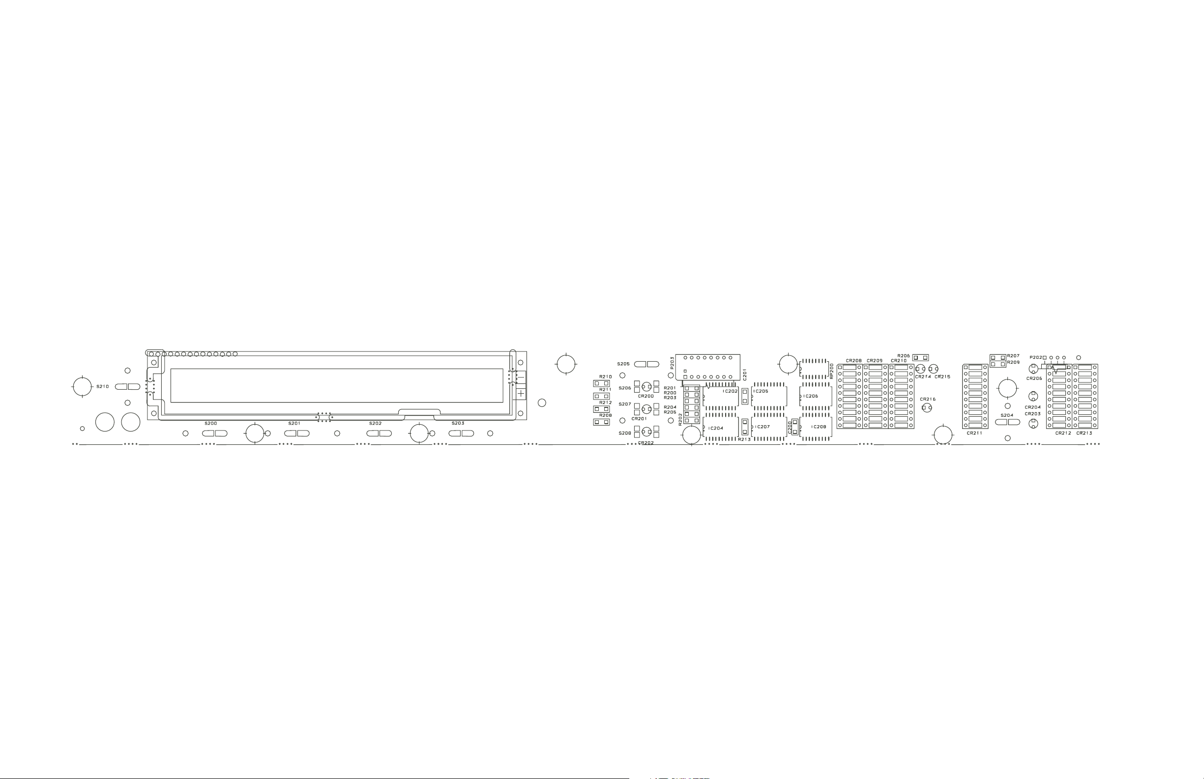
6-44
TECHNICAL DATA Orban Model 2200
Display Board version 1
Drawing 31875.000.01
Reference schematic 61182.000.01
Page 47
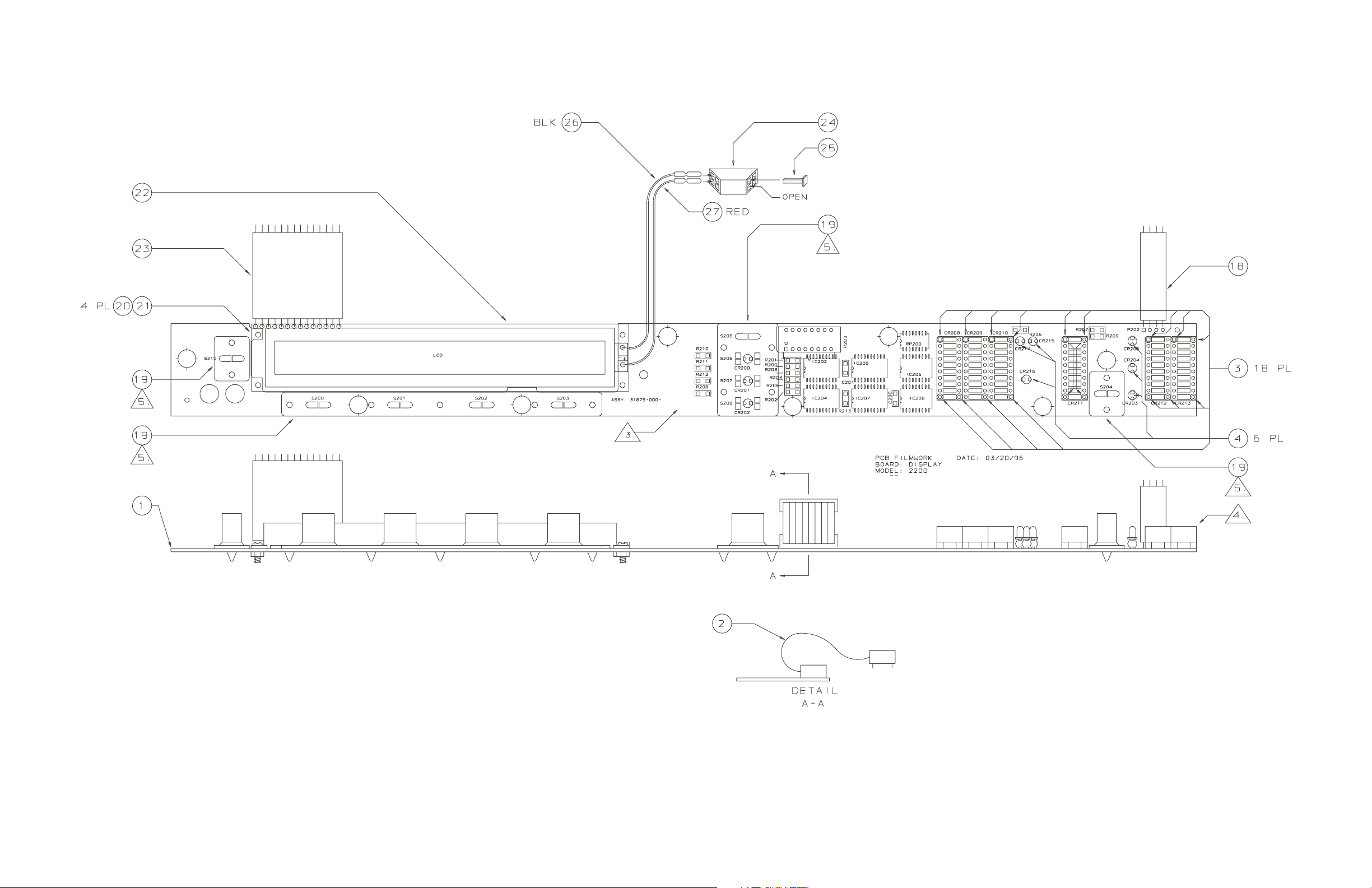
OPTIMOD-FM DIGITAL TECHNICAL DATA
6-45
Display Board version 2
Drawing 31875.000.01
Reference schematic 61182.000.01
Page 48
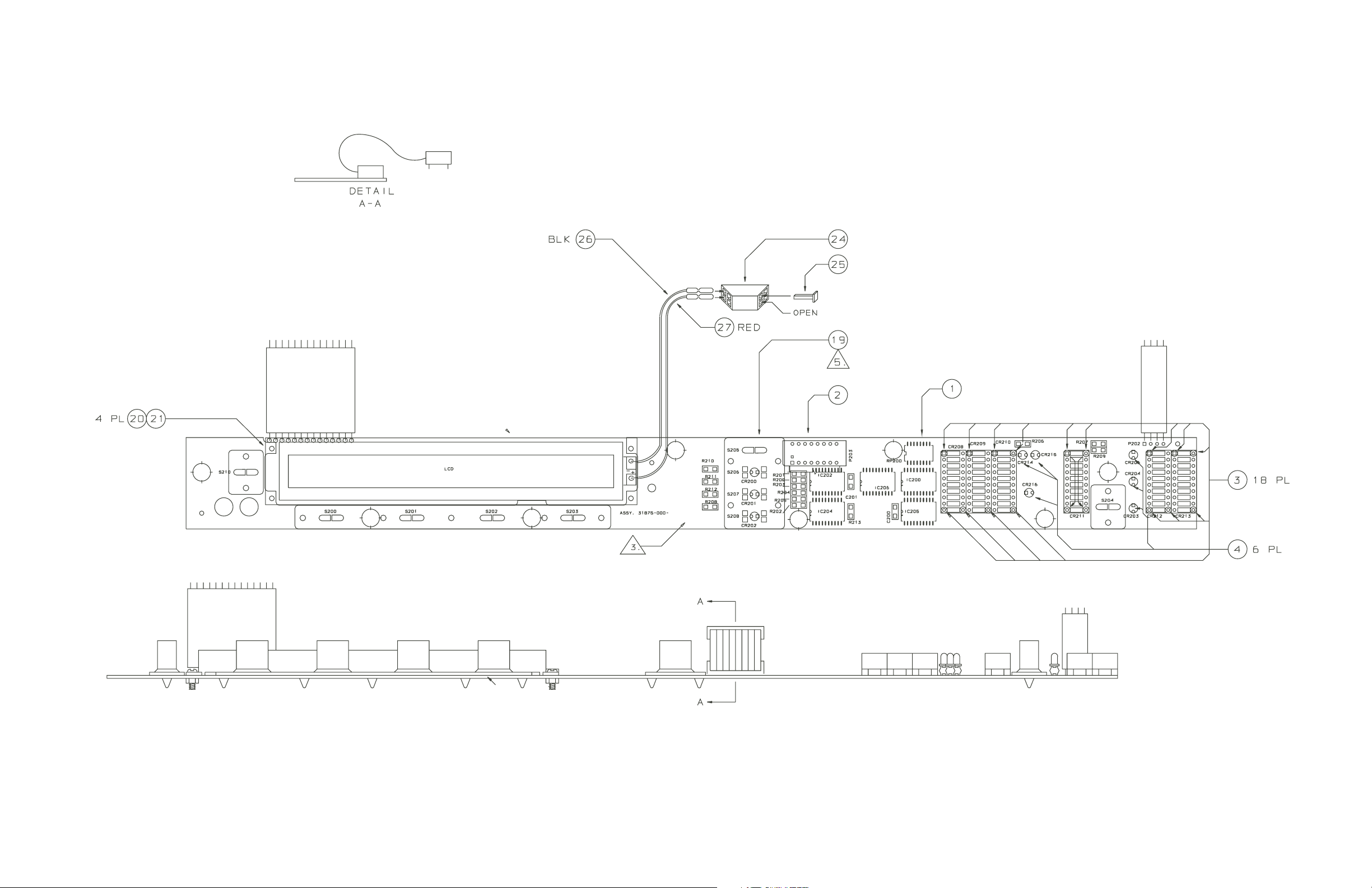
6-46
TECHNICAL DATA Orban Model 2200
Display Board version 3
Drawing 31875.000.08
Reference schematic 61182.000.03
Page 49
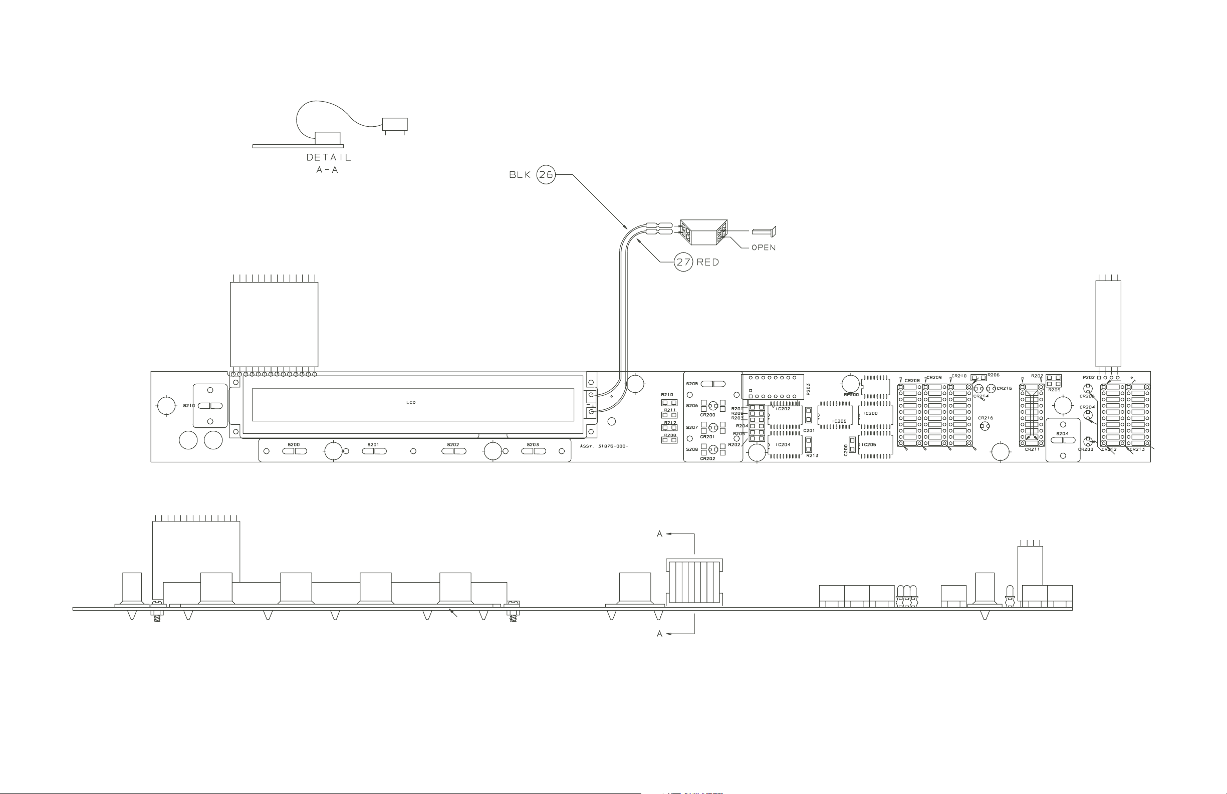
OPTIMOD-FM DIGITAL TECHNICAL DATA
6-47
Display Board version 4
Drawing 31875.000.09
reference schematic 61182.000.03
Page 50
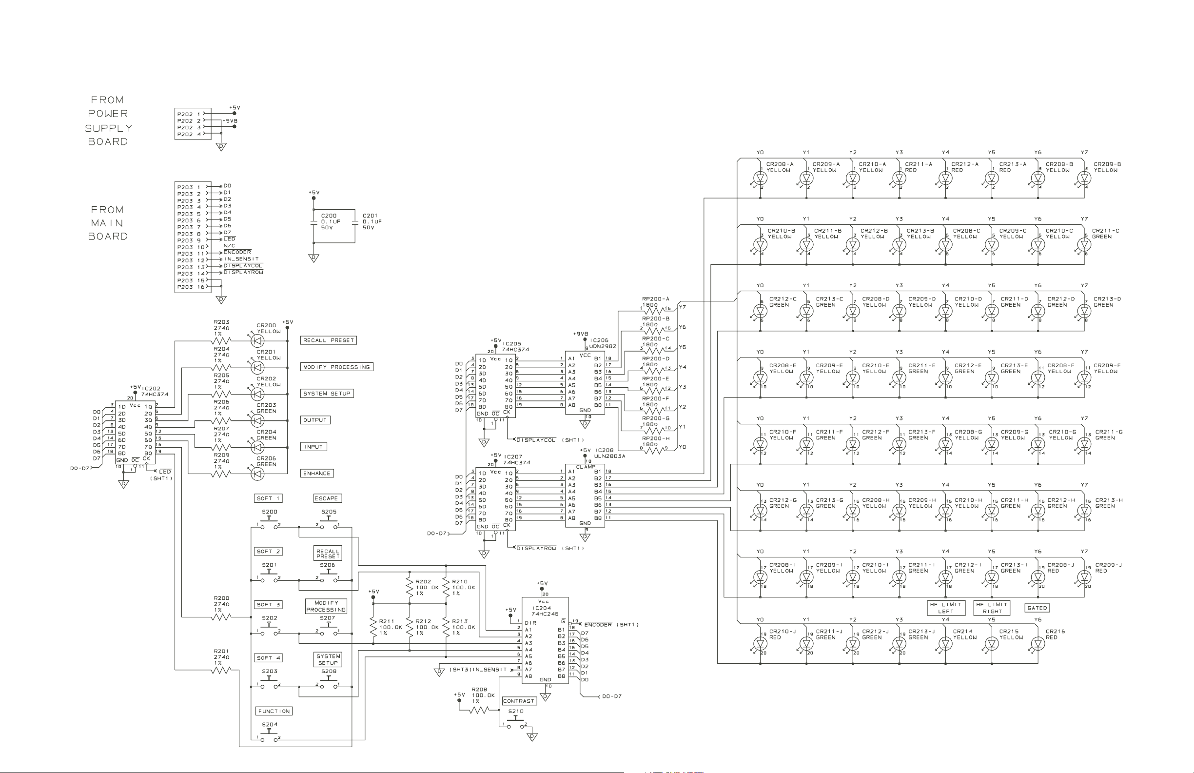
6-48
TECHNICAL DATA Orban Model 2200
Display Board version 1
schematic 61182-000-01
Page 51
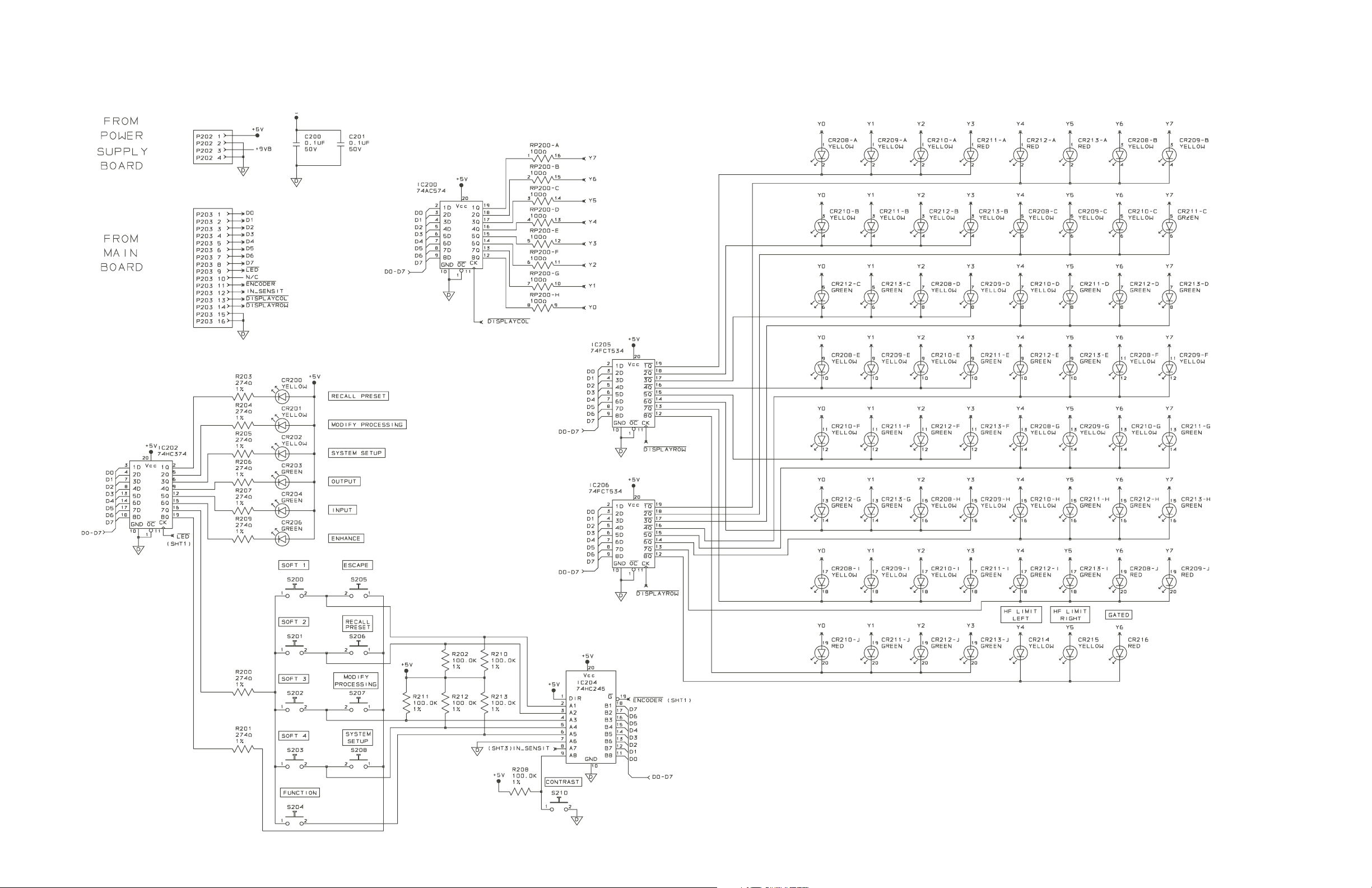
OPTIMOD-FM DIGITAL TECHNICAL DATA
6-49
Display Board version 2
schematic 61182-000-02
Page 52
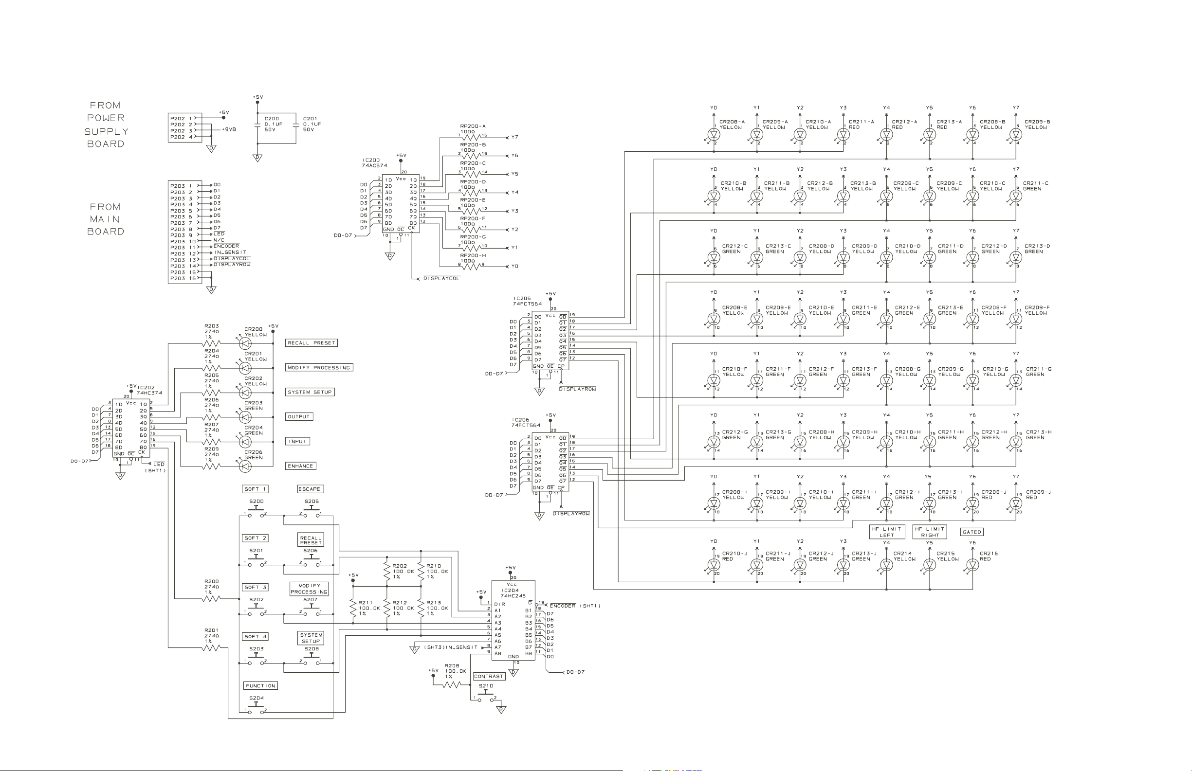
6-50
TECHNICAL DATA Orban Model 2200
Display Board version 3
schematic 61182-000-03
Page 53
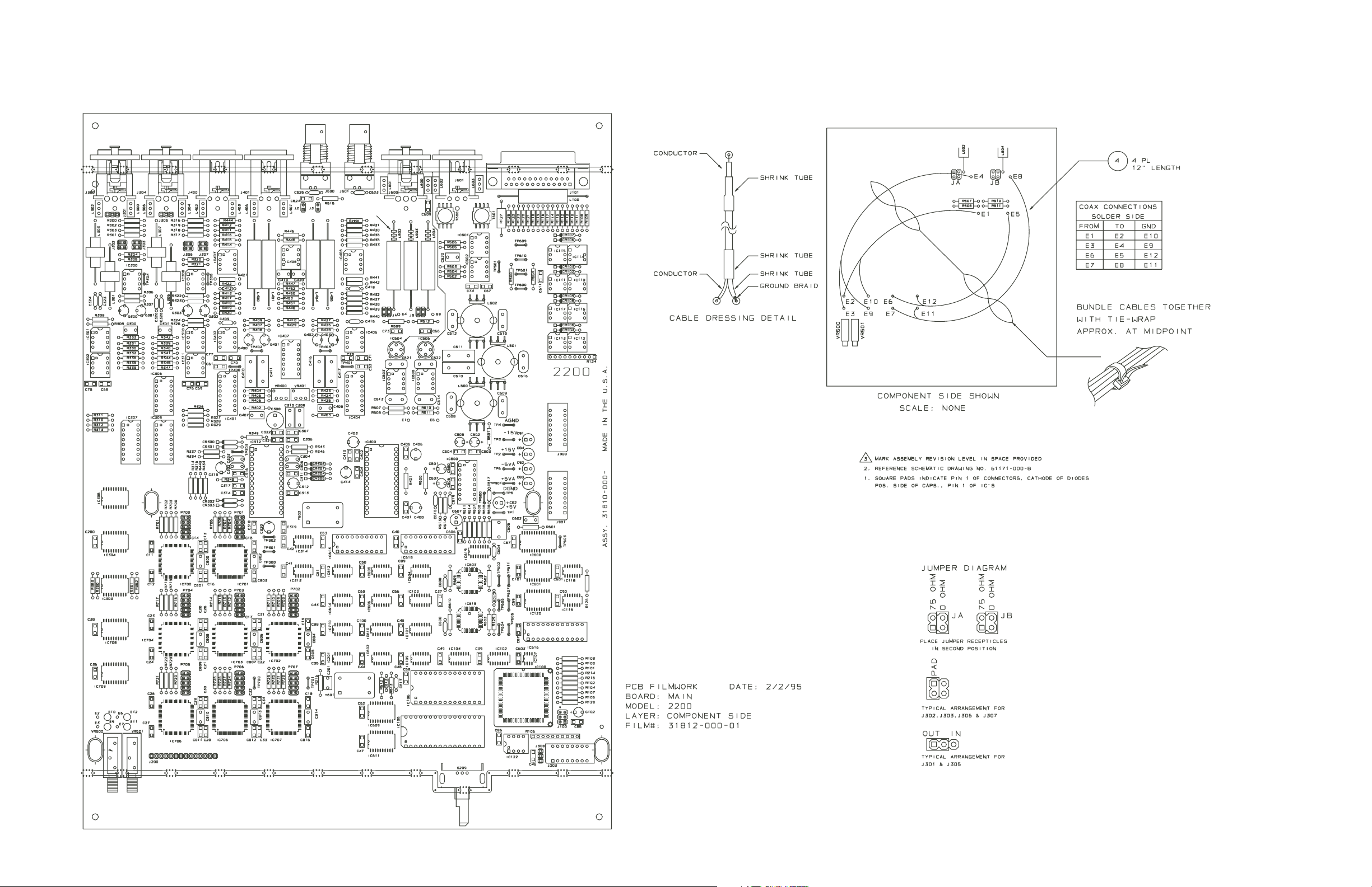
OPTIMOD-FM DIGITAL TECHNICAL DATA
6-51
Main Board version 1 (1 of 2)
reference schematic 61171-000-8
Page 54
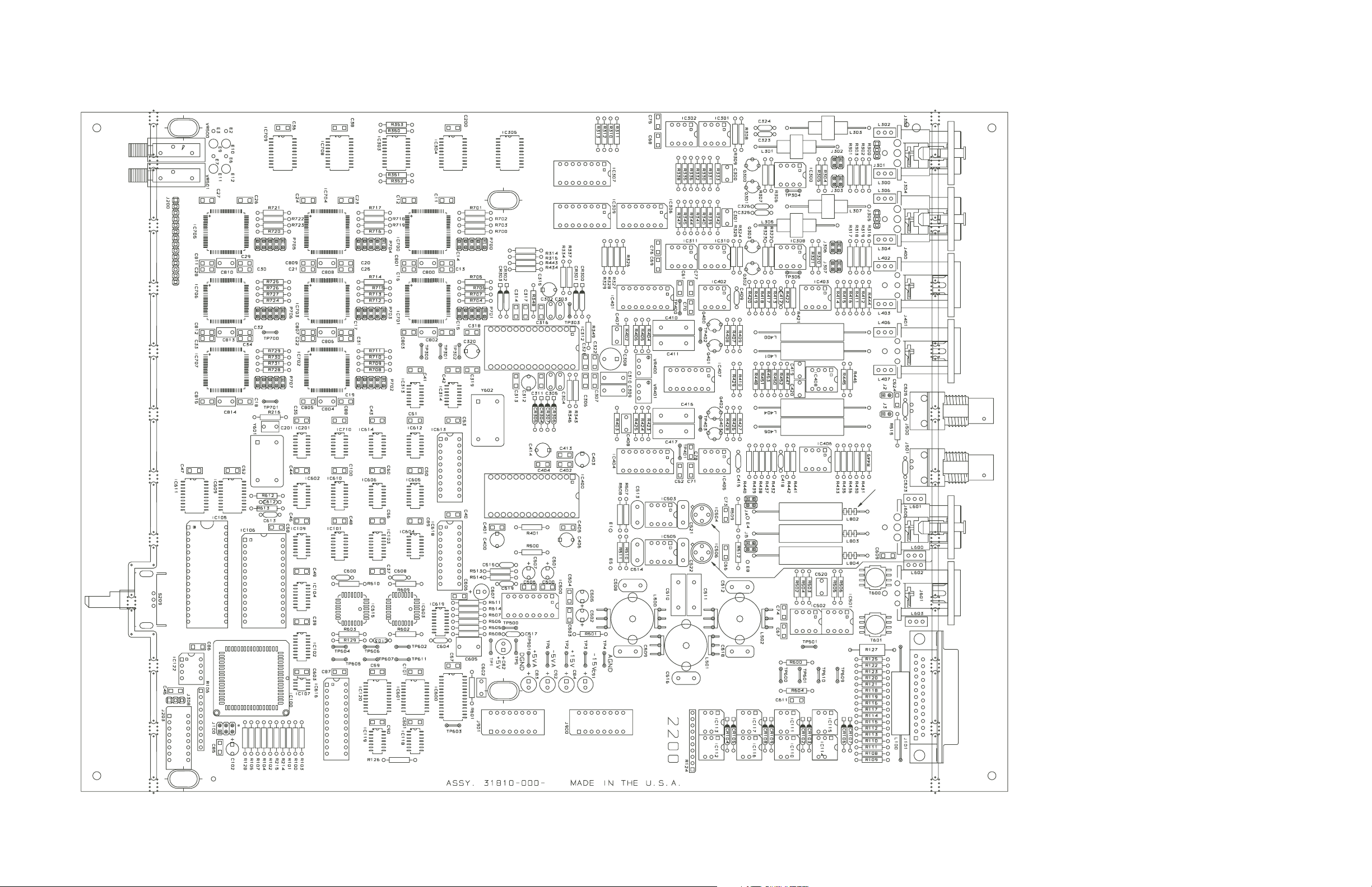
6-52
TECHNICAL DATA Orban Model 2200
Main Board version 1 (detail: 2 of 2)
reference schematic 61171-000-8
Page 55
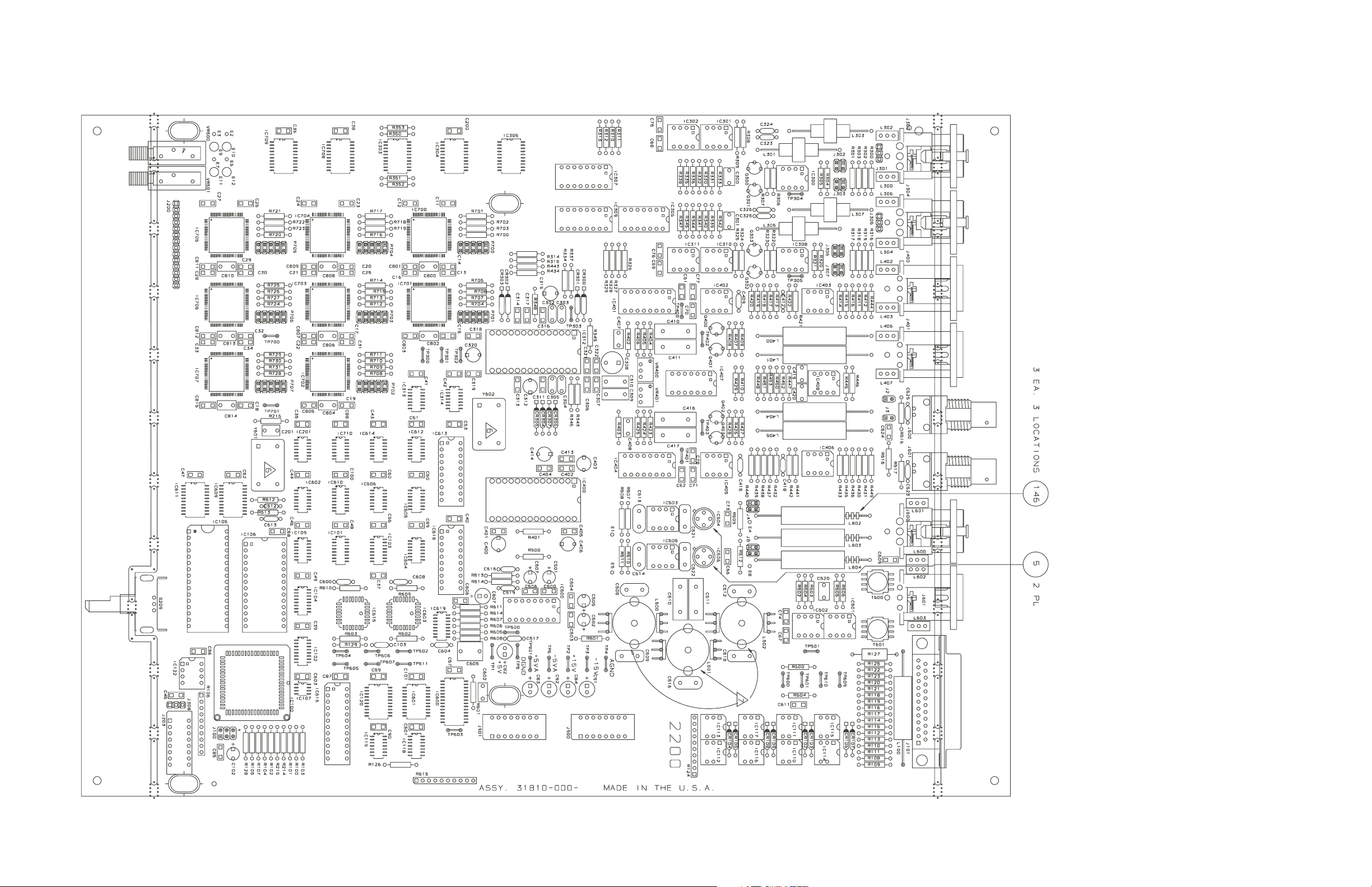
OPTIMOD-FM DIGITAL TECHNICAL DATA
6-53
Main Board version 2
reference schematic 61171-000-
Page 56
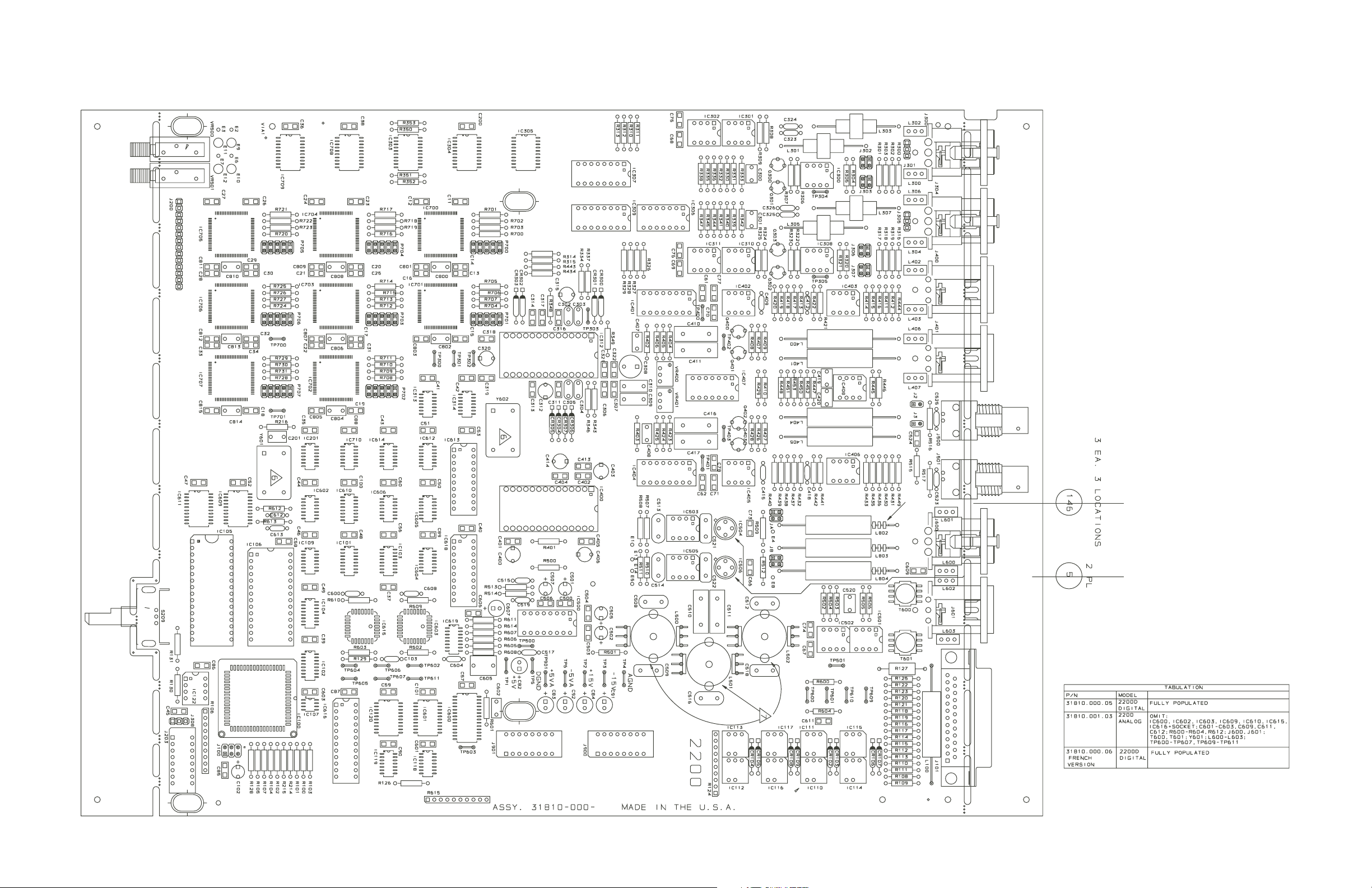
6-54
TECHNICAL DATA Orban Model 2200
Main Board version 3
reference schematic 61171-000-
Page 57
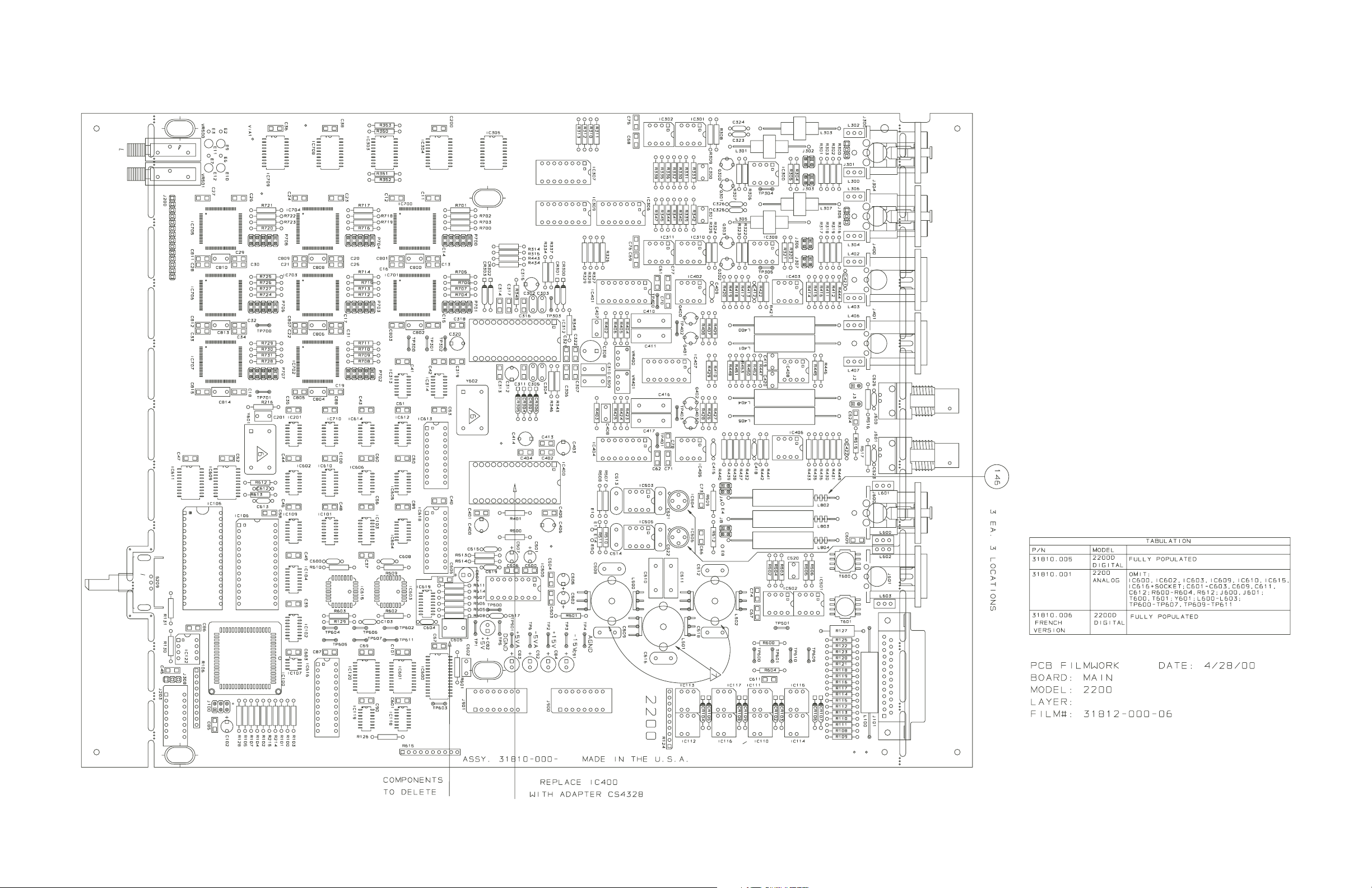
OPTIMOD-FM DIGITAL TECHNICAL DATA
6-55
Main Board version 4
reference schematic 61171-000-
Page 58
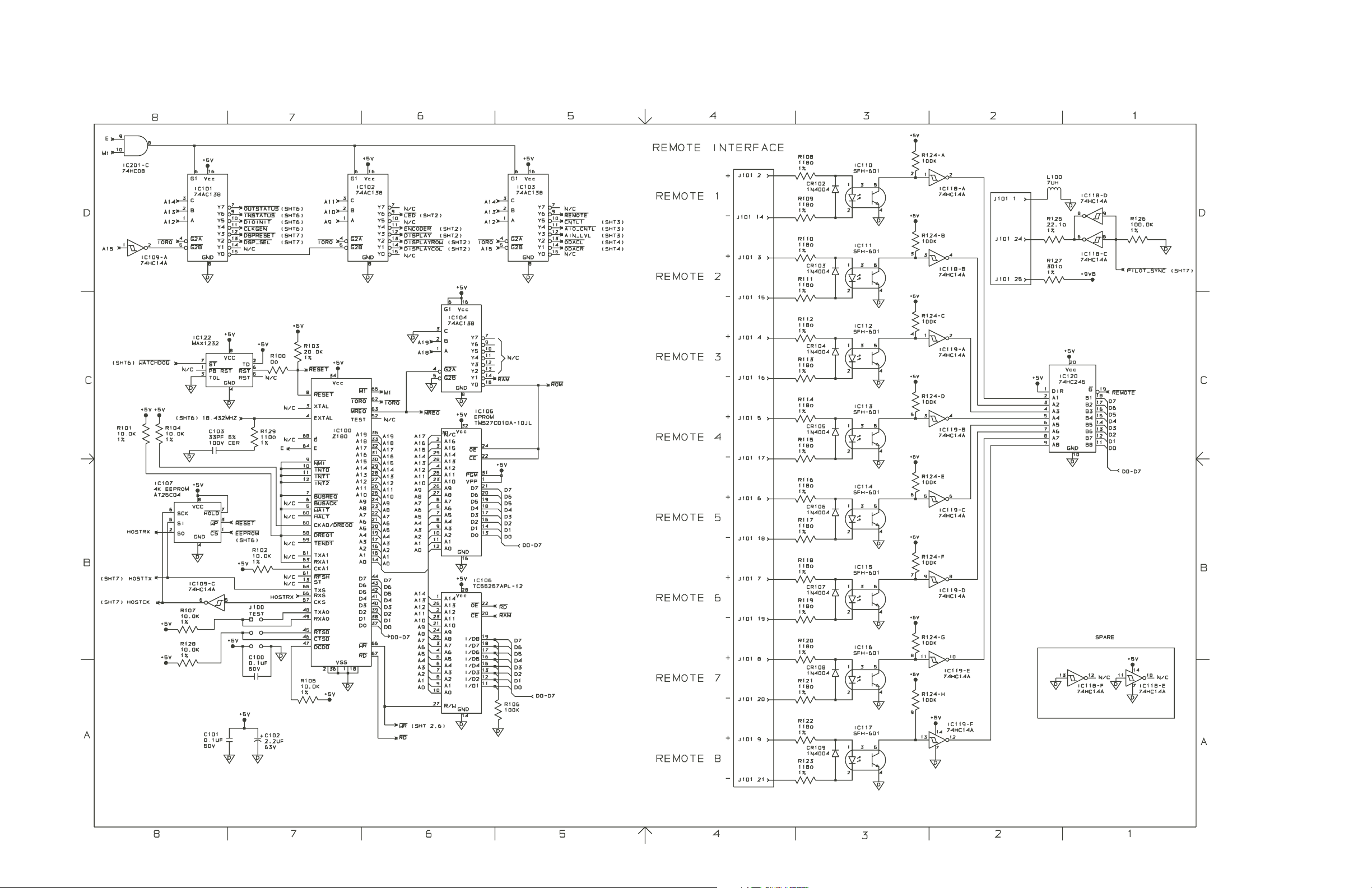
6-56
TECHNICAL DATA Orban Model 2200
Main Board: CPU/Remote version 1
schematic 61171.000.01
(sheet 1 of 9)
Page 59
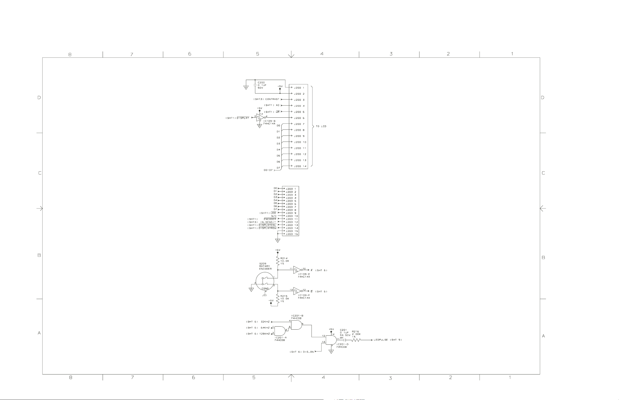
OPTIMOD-FM DIGITAL TECHNICAL DATA
6-57
Main Board: Display version 1
schematic 61171.000.01
(sheet 2 of 9)
Page 60
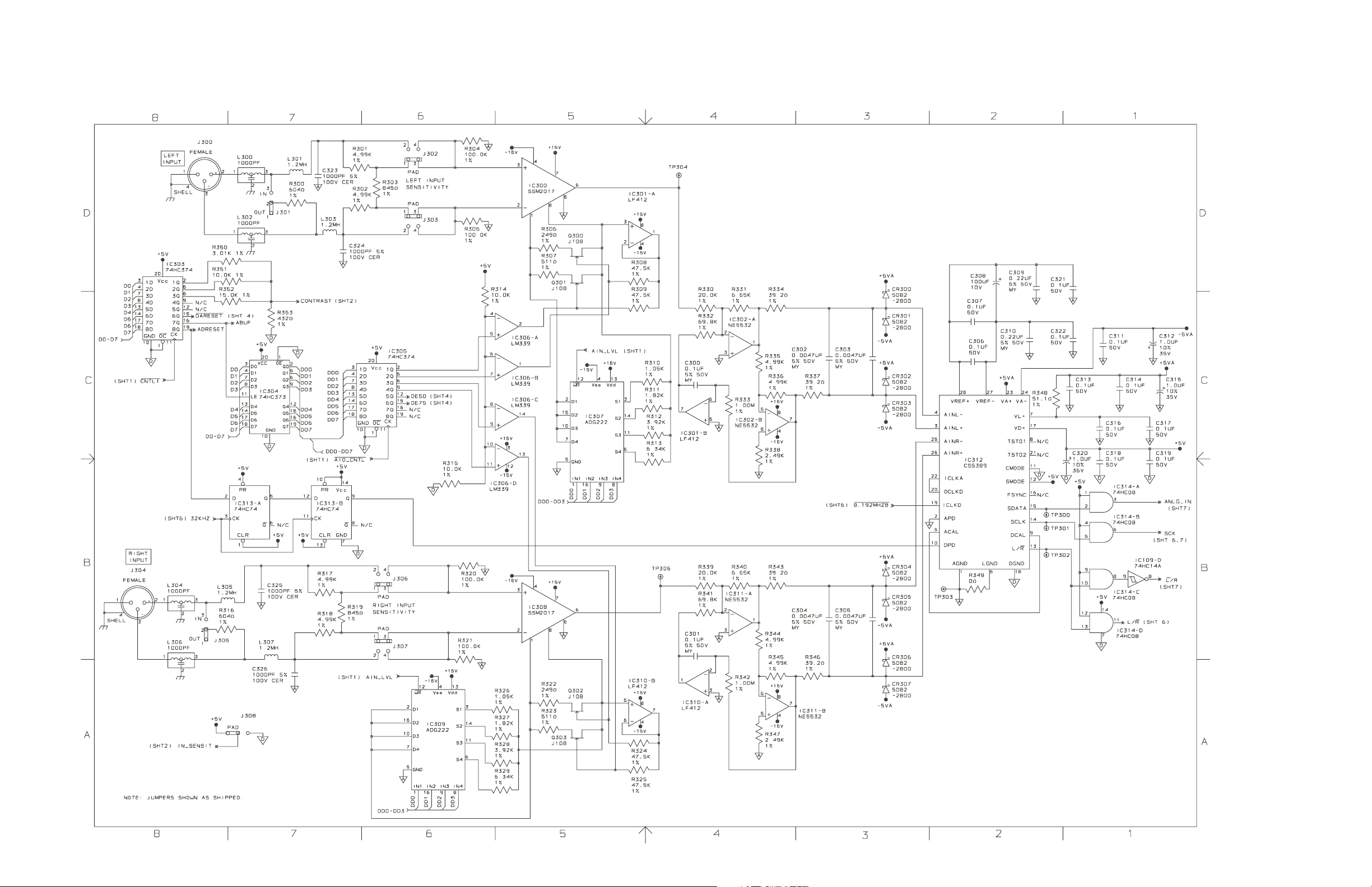
6-58
TECHNICAL DATA Orban Model 2200
Main Board: Analog Input version 1
schematic 61171.000.01
(sheet 3 of 9)
Page 61
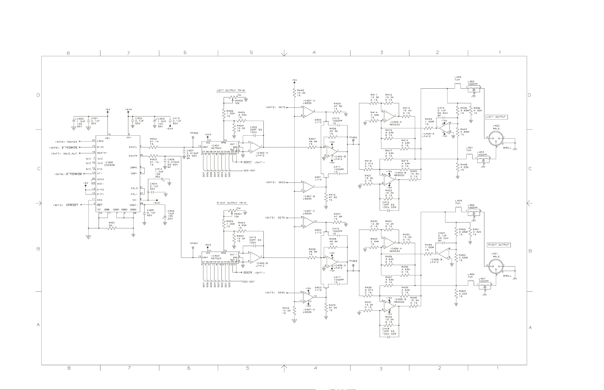
OPTIMOD-FM DIGITAL TECHNICAL DATA
6-59
Main Board: Analog Output version 1
schematic 61171.000.01
(sheet 4 of 9)
Page 62
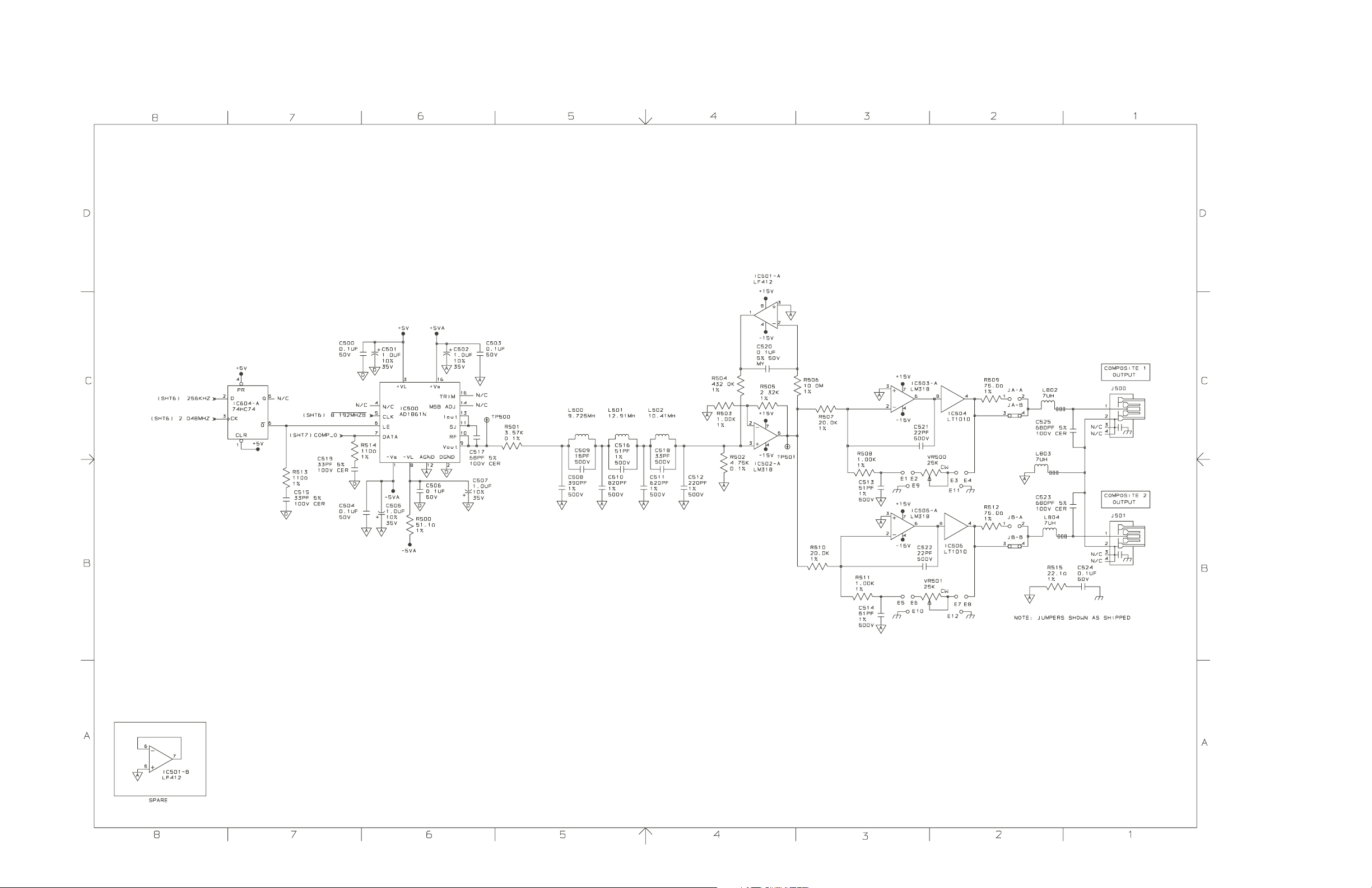
6-60
TECHNICAL DATA Orban Model 2200
Main Board: Composite Output version 1
schematic 61171.000.01
(sheet 5 of 9)
Page 63
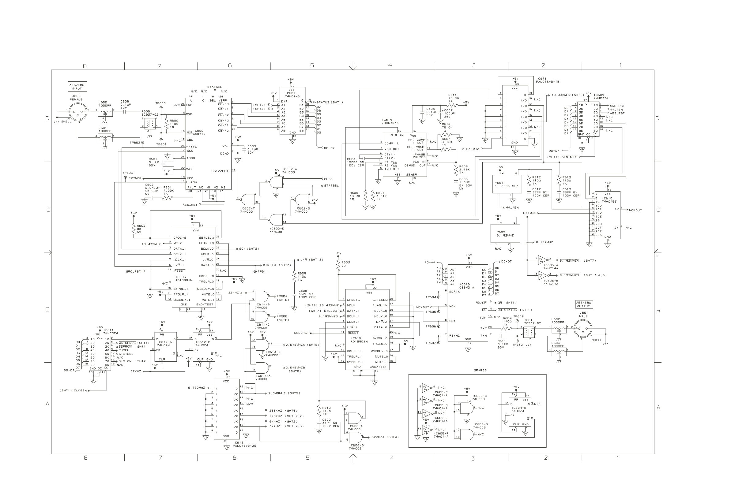
OPTIMOD-FM DIGITAL TECHNICAL DATA
6-61
Main Board: Digital I/O version 1
schematic 61171.000.01
(sheet 6 of 9)
Page 64
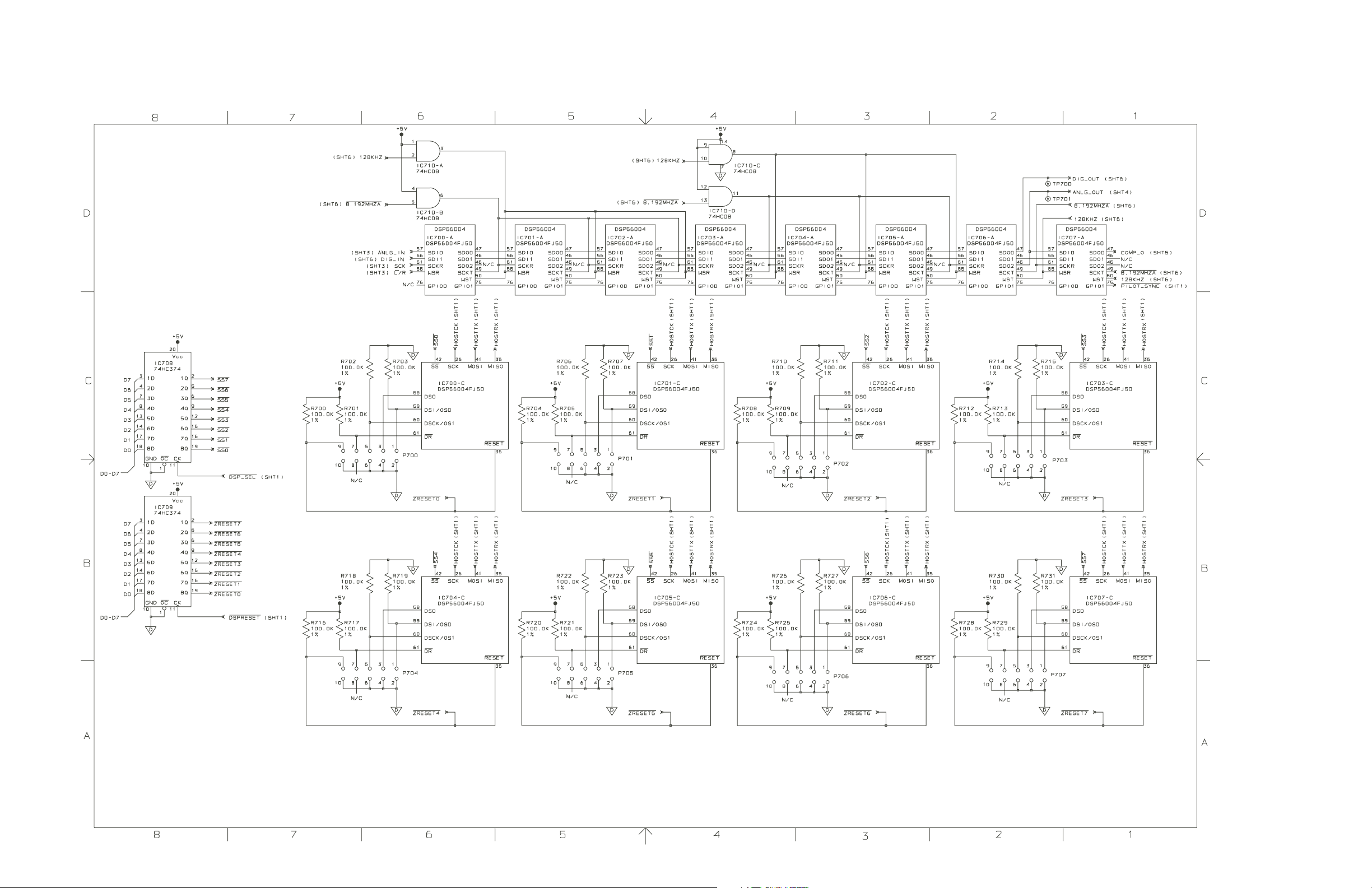
6-62
TECHNICAL DATA Orban Model 2200
Main Board: DSP 1 version 1
schematic 61171.000.01
(sheet 7 of 9)
Page 65
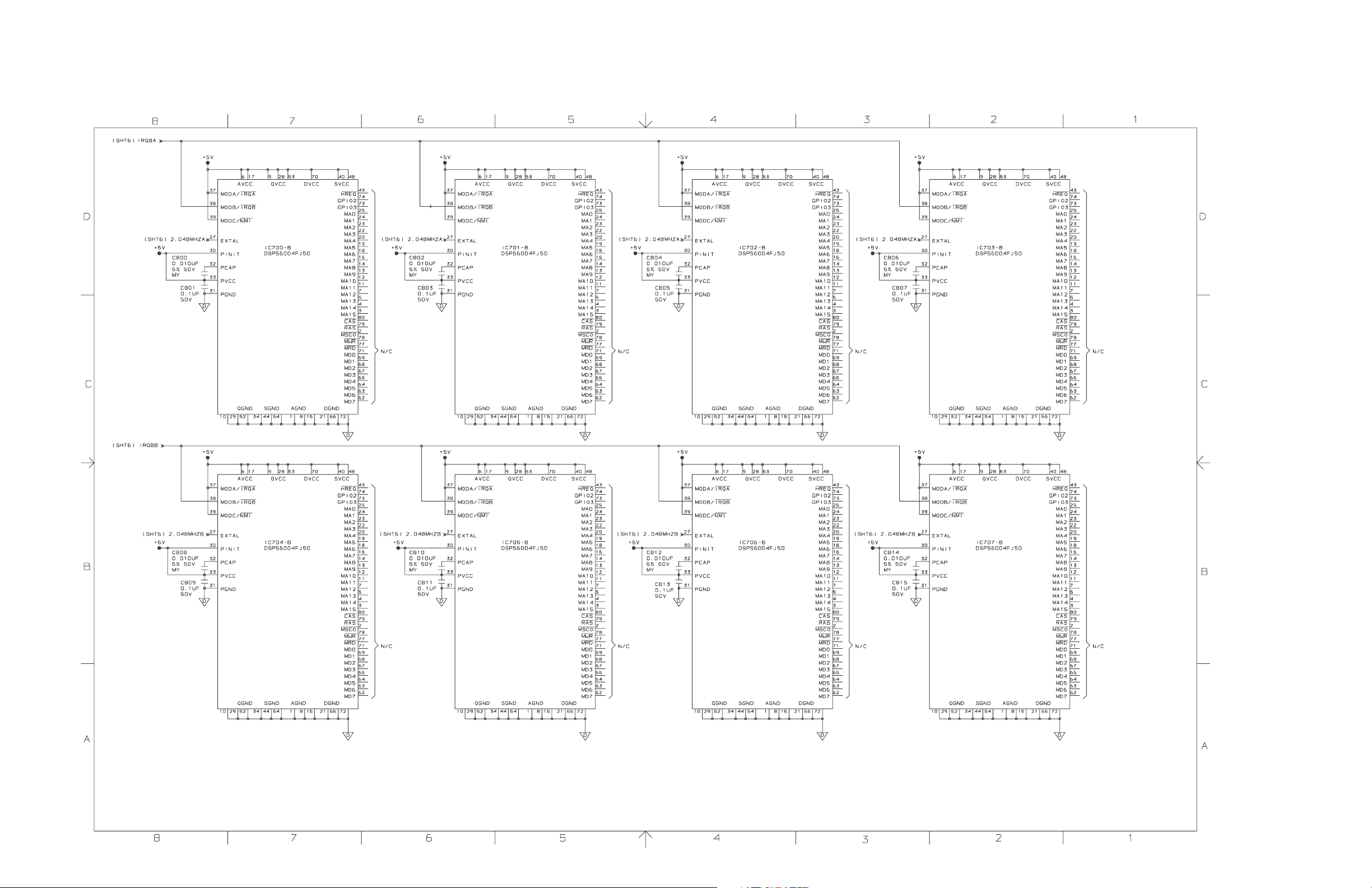
OPTIMOD-FM DIGITAL TECHNICAL DATA
6-63
Main Board: DSP 2 version 1
schematic 61171.000.01
(sheet 8 of 9)
Page 66
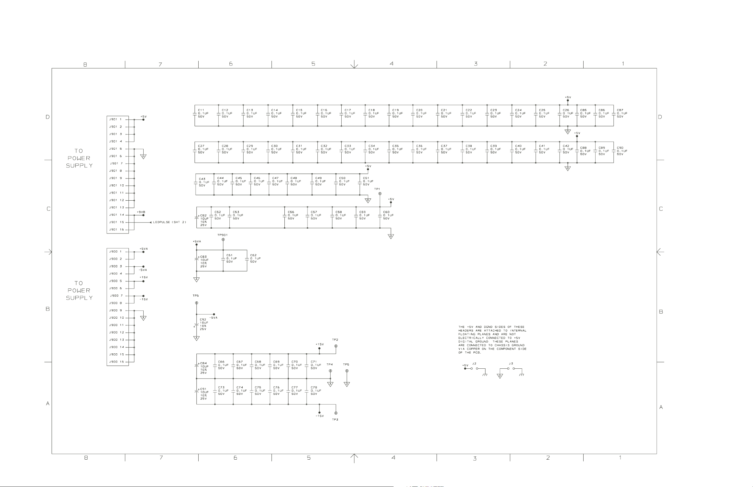
6-64
TECHNICAL DATA Orban Model 2200
Main Board: Power Distribution version 1
schematic 61171.000.01
(sheet 9 of 9)
Page 67
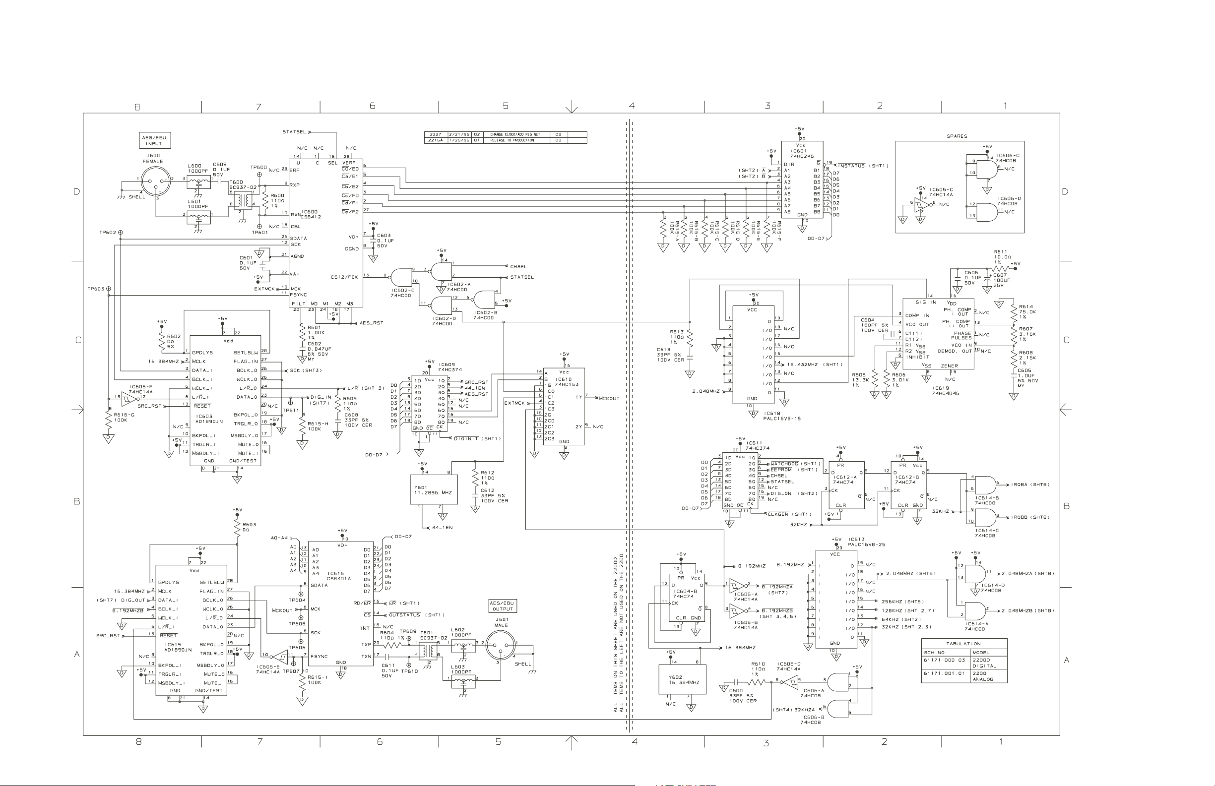
OPTIMOD-FM DIGITAL TECHNICAL DATA
6-65
Main Board: Digital I/O version 2
schematic 61171.000.0x (see tabulation)
(sheet 6 of 9)
Page 68
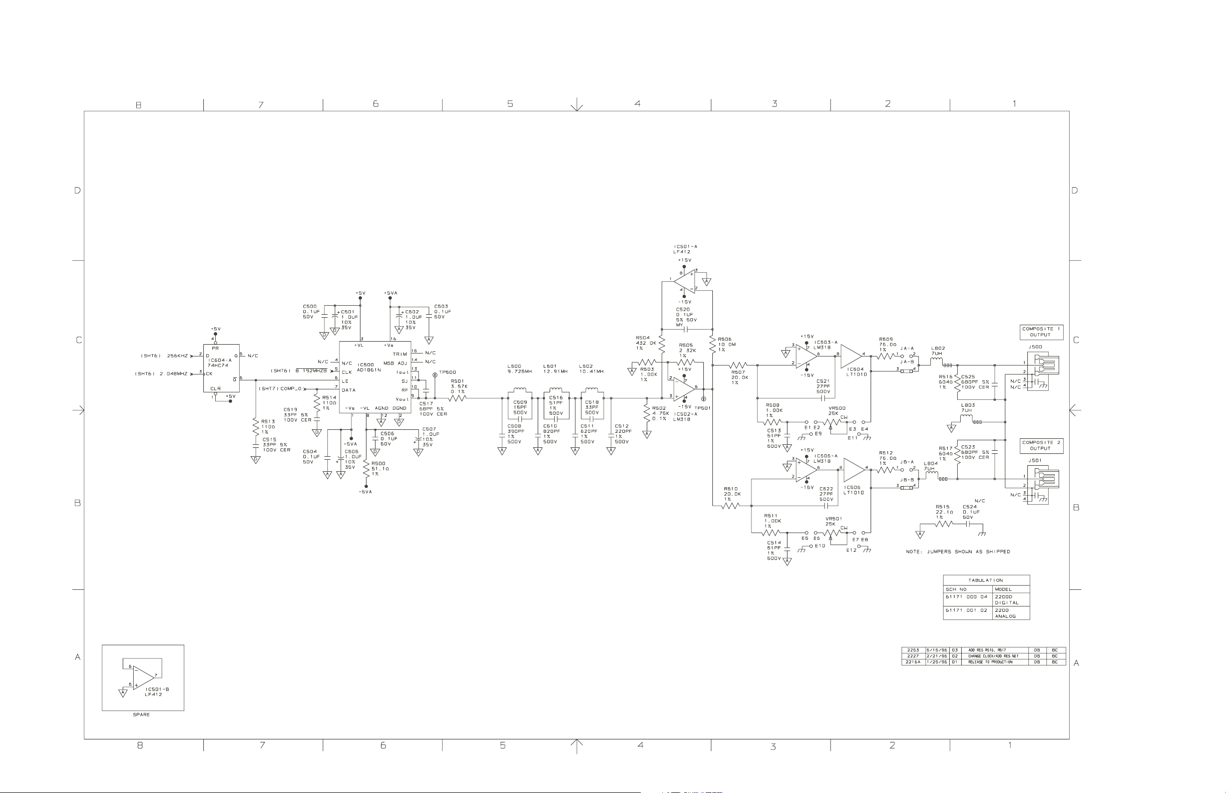
6-66
TECHNICAL DATA Orban Model 2200
Main Board: Composite Ouput version 3
schematic 61171.000.0x (see tabulation)
(sheet 5 of 9)
Page 69
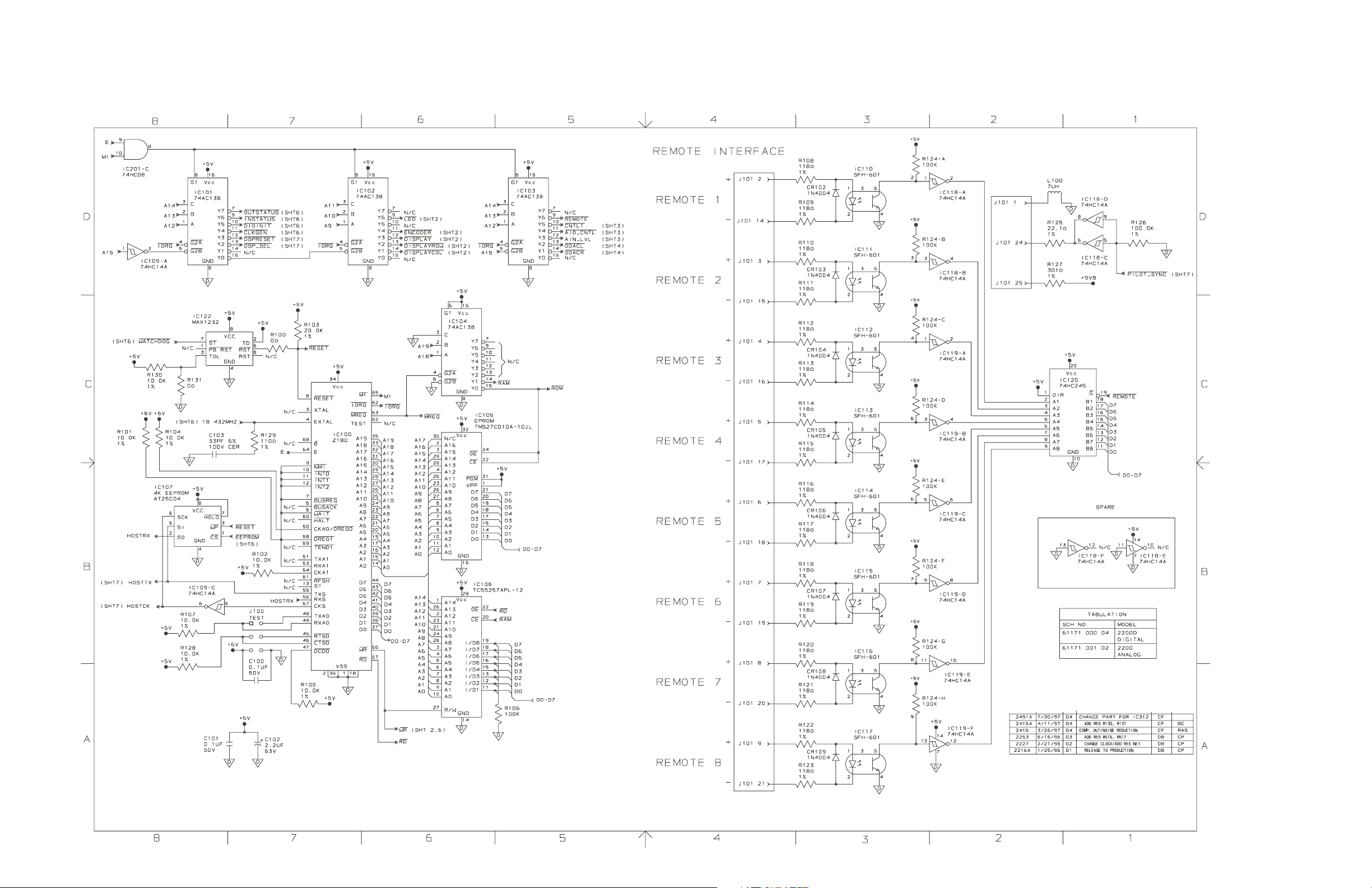
OPTIMOD-FM DIGITAL TECHNICAL DATA
6-67
Main Board: CPU/Remote version 4
schematic 61171.000.0x (see tabulation)
(sheet 1 of 9)
Page 70
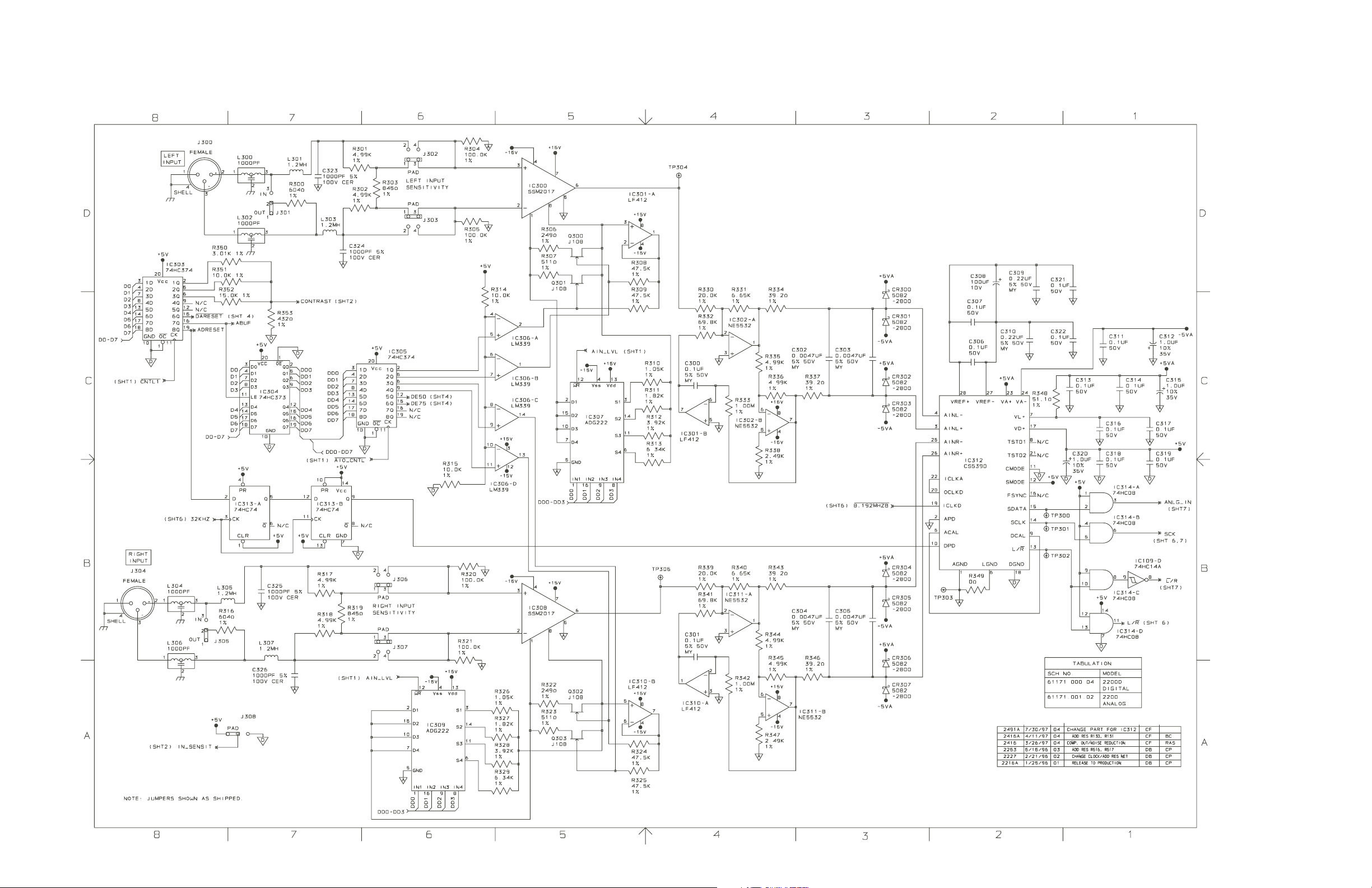
6-68
TECHNICAL DATA Orban Model 2200
Main Board: Analog Input version 4
schematic 61171.000.0x (see tabulation)
(sheet 3 of 9)
Page 71
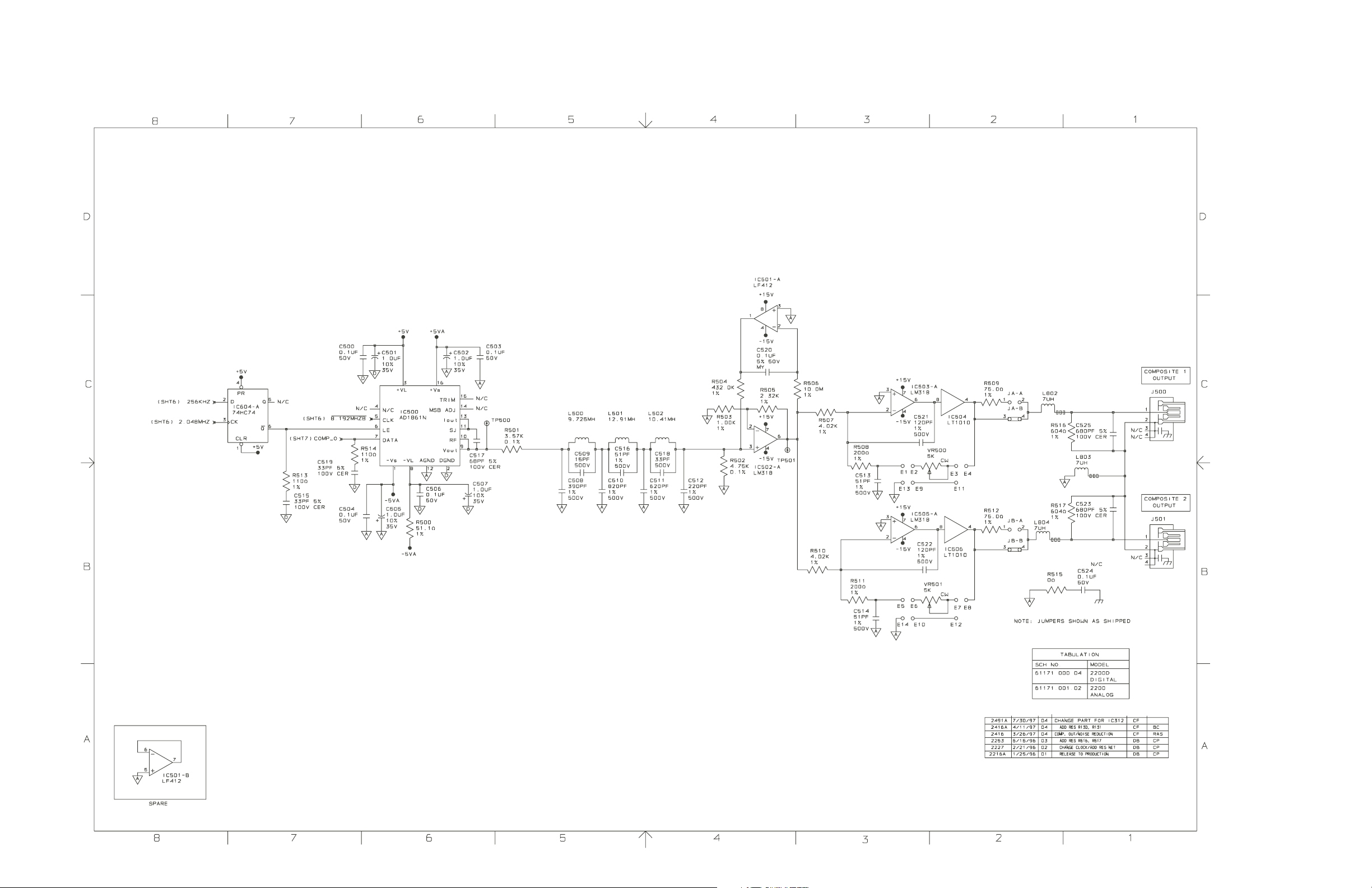
OPTIMOD-FM DIGITAL TECHNICAL DATA
6-69
Main Board: Composite Output version 4
schematic 61171.000.0x (see tabulation)
(sheet 5 of 9)
Page 72
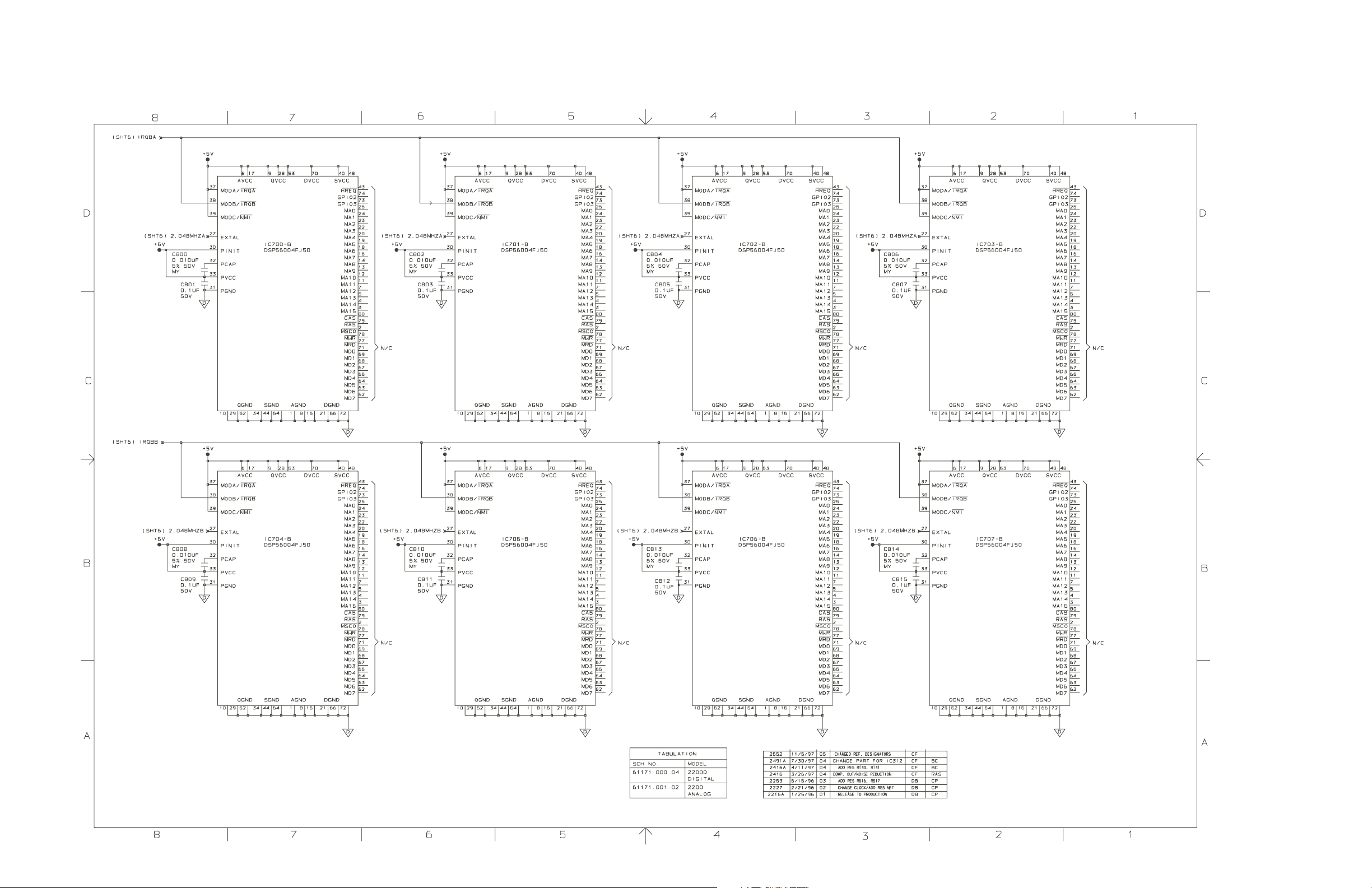
6-70
TECHNICAL DATA Orban Model 2200
Main Board: DSP 2 version 5
schematic 61171.000.0x (see tabulation)
(sheet 8 of 9)
Page 73
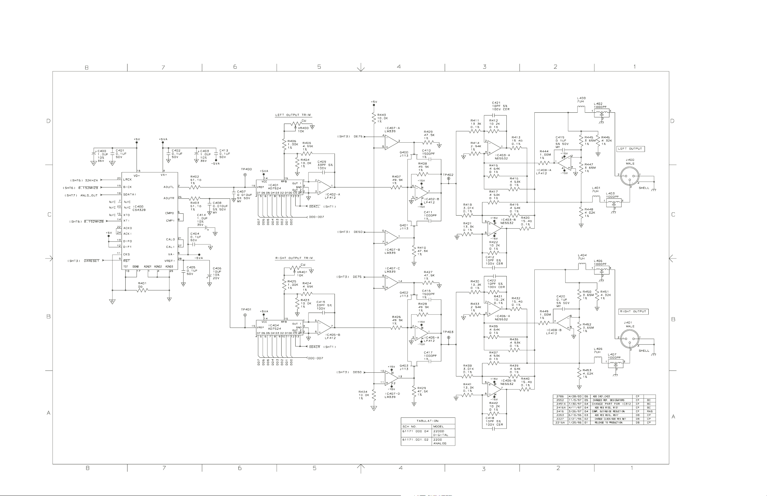
OPTIMOD-FM DIGITAL TECHNICAL DATA
6-71
Main Board: Analog Output version 6
schematic 61171.000.0x (see tabulation)
(sheet 4 of 9)
Page 74
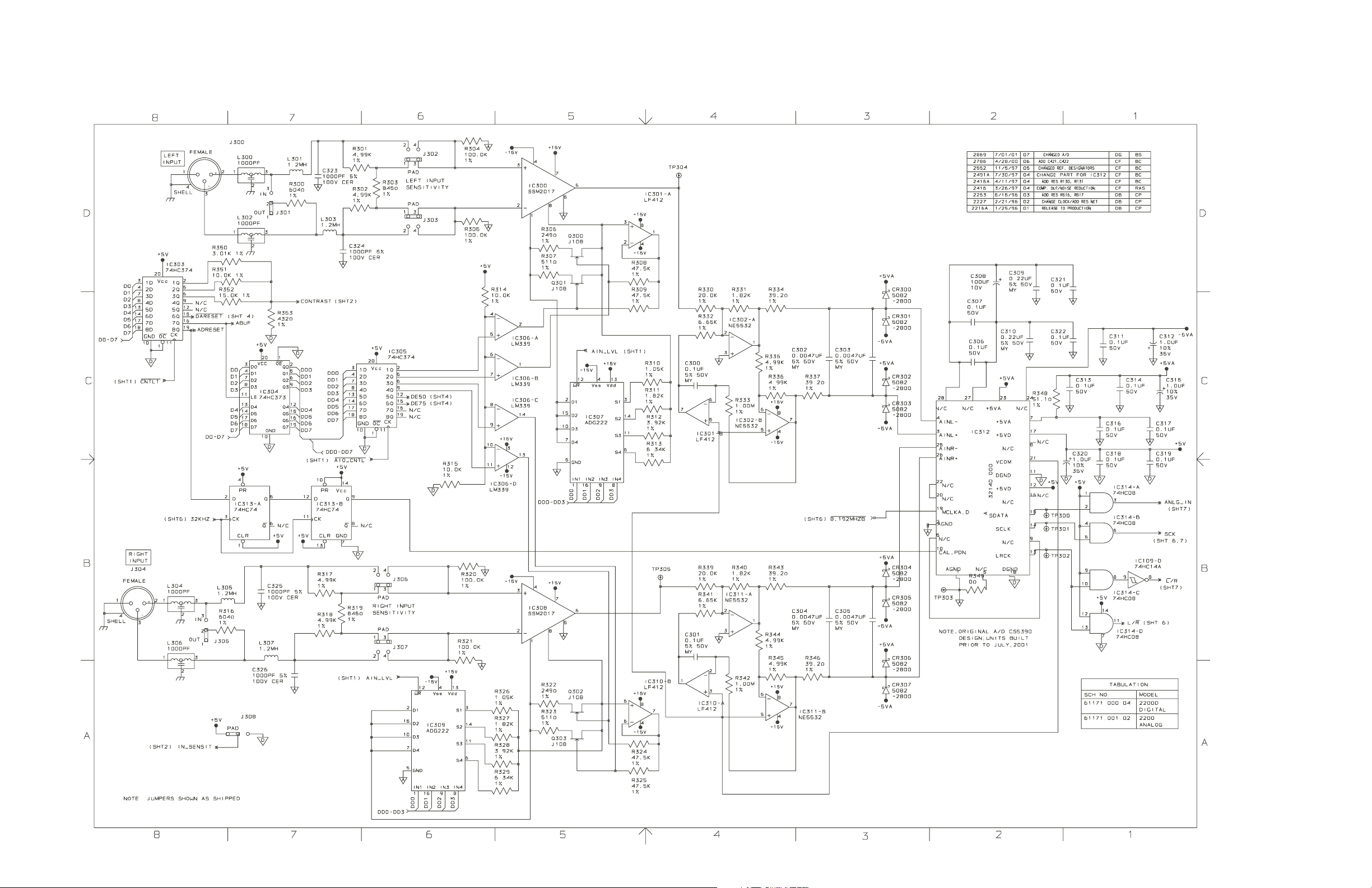
6-72
TECHNICAL DATA Orban Model 2200
Main Board: Analog Input version 7
schematic 61171.000.0x (see tabulation)
(sheet 3 of 9)
Page 75
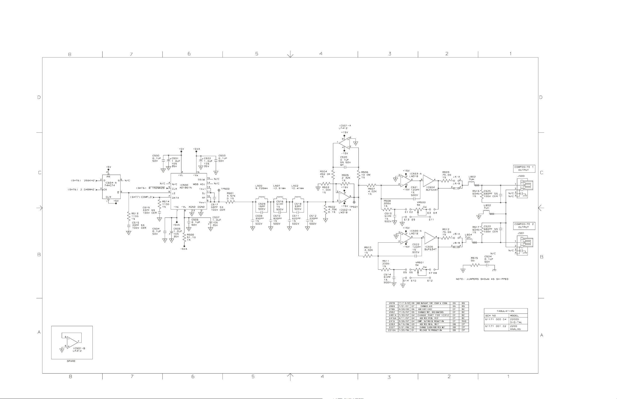
OPTIMOD-FM DIGITAL TECHNICAL DATA
6-73
Main Board: Composite Output version 8
schematic 61171.000.0x (see tabulation)
(sheet 5 of 9)
Page 76
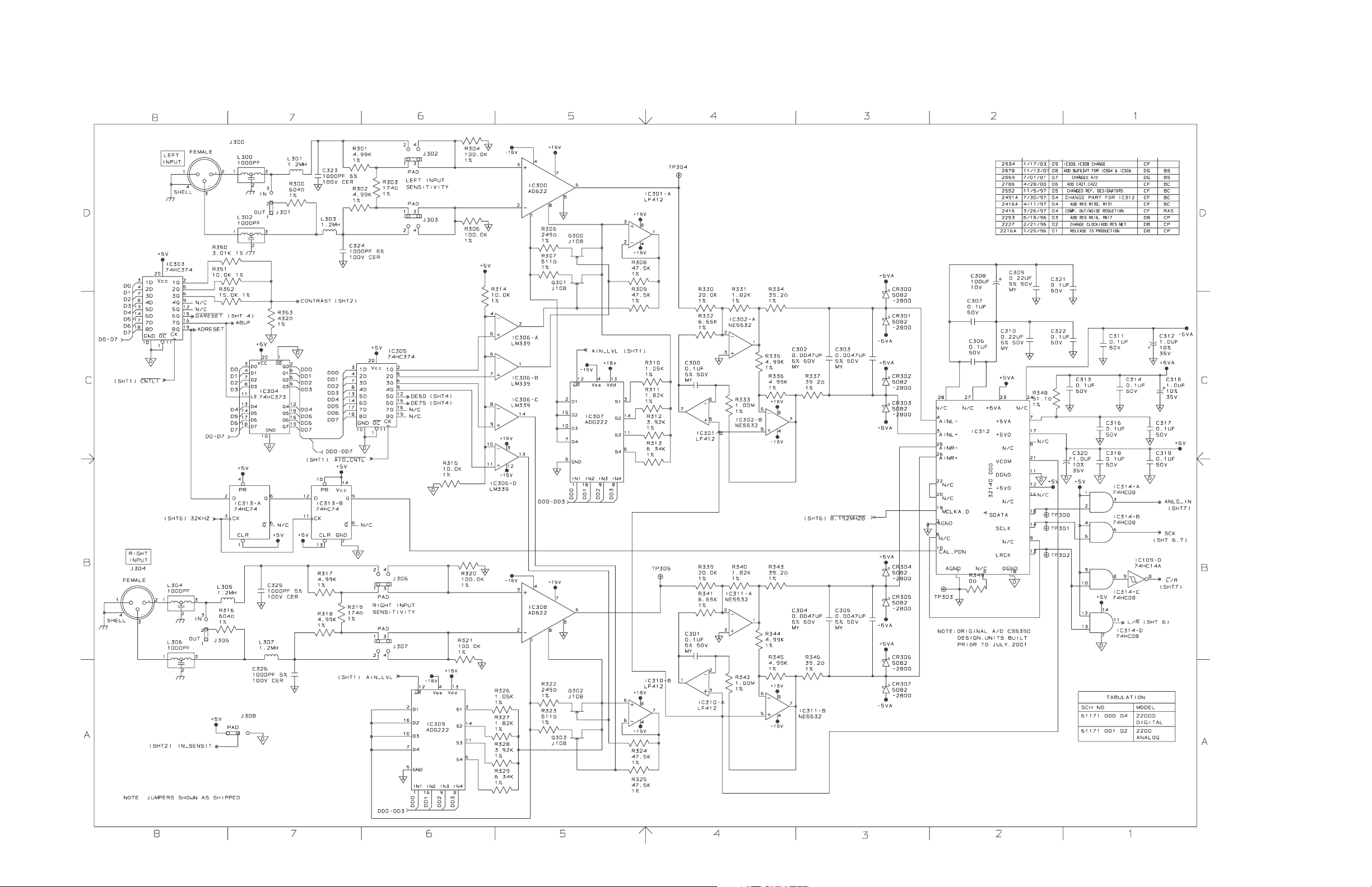
6-74
TECHNICAL DATA Orban Model 2200
Main Board: Analog Input version 9
schematic 61171.000.0x (see tabulation)
(sheet 3 of 9)
Page 77
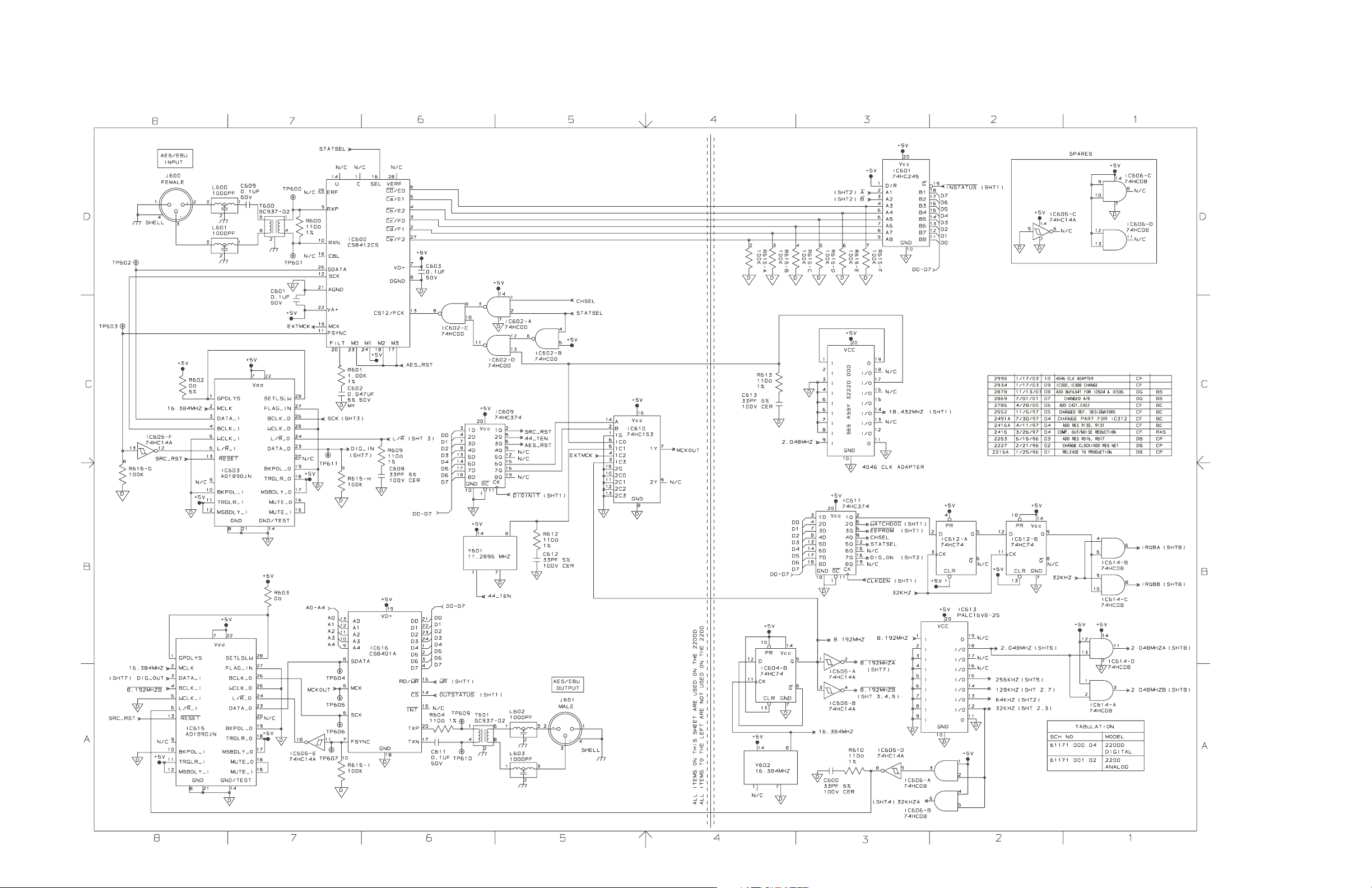
OPTIMOD-FM DIGITAL TECHNICAL DATA
6-75
Main Board: Digital I/O version 10
schematic 61171.000.0x (see tabulation)
(sheet 6 of 9)
Page 78
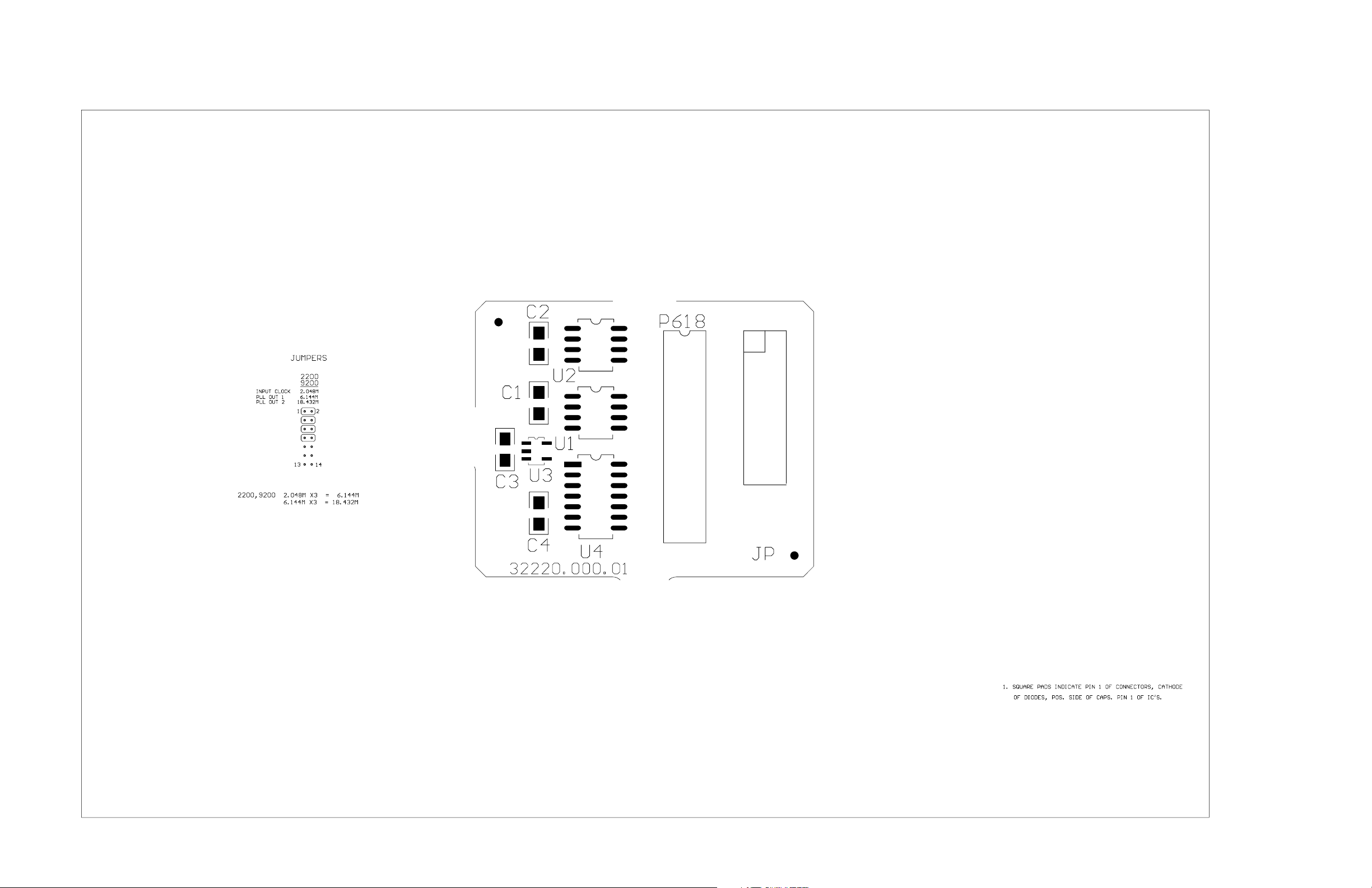
6-76
TECHNICAL DATA Orban Model 2200
Clock Generator version 1
Drawing 32220.000.01
Reference schematic 62220.000.01
Page 79
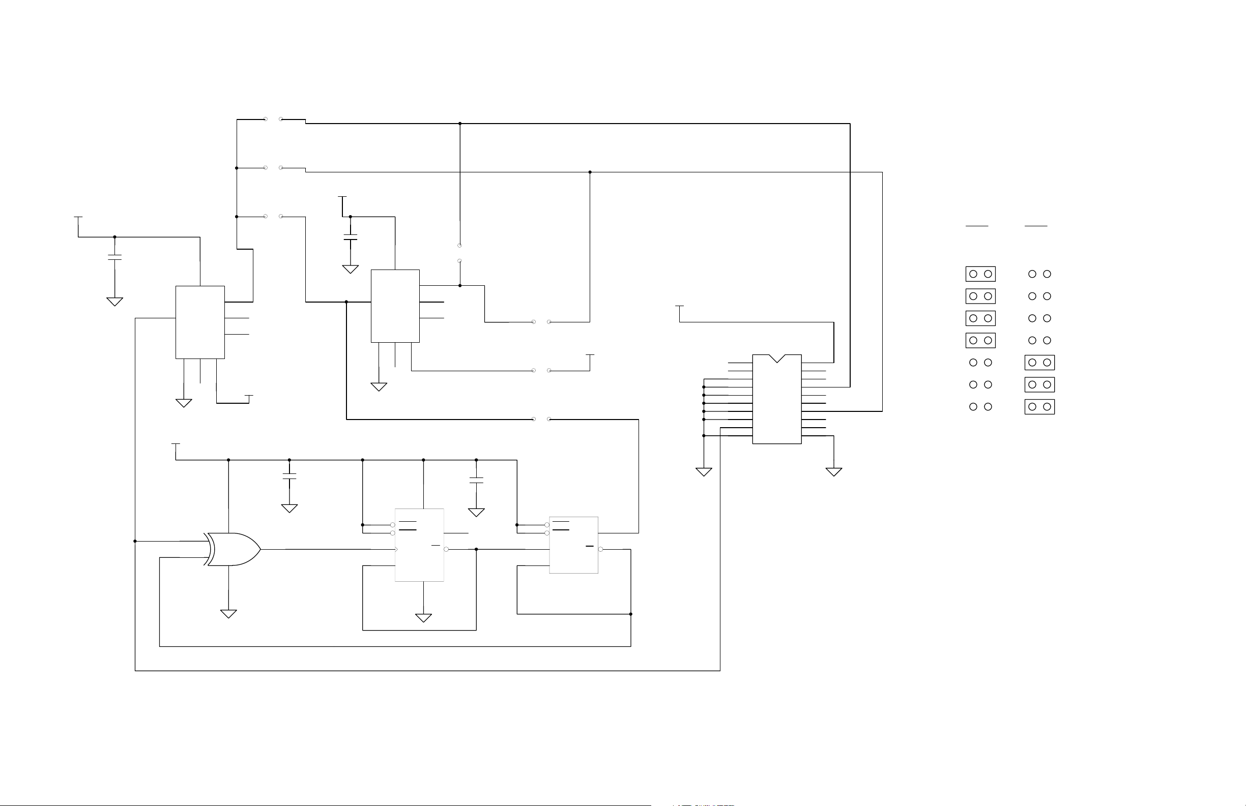
OPTIMOD-FM DIGITAL TECHNICAL DATA
JP-A
1 2
9 10
JUMPERS
+5
6-77
+5
C1
CAP_.01UF
D
1
+5
ICLK
GND
3
D
1
2
N/C
2
CLK
VDD
OE
X2
S1
4S06
U1
5
7
8
ICS501
X3
5
3
3 4
N/C
N/C
+5
U3
4
AHCT86
C3
CAP_.01UF
D
C2
CAP_.01UF
D
1
ICLK
GND
3
D
4
1
3
2
2
N/C
CLK
VDD
OE
X2
1 PRE
1 CLR
1 CLK
1D
4S06
U2
S1
ICS501
14
7
5
7
8
X3/X2
VCC
1Q
1Q
GND
11 12
N/C
N/C
U4A
5
6
AHCT74
JP-C
D
N/C
C4
CAP_.01UF
JP-B
5 6
7 8
14 13
10
2PRE
13
2CLR
11
2CLK
12
2D
+5
2Q
2Q
U4B
9
8
AHCT74
+5
P618
1
2
3
4
5
6
7
8
9
10 11
20PIN-ADAPTER
D D
INPUT CLOC K 2.048M 6.144M
PLL OUT 1 6.144M 4.096M
PLL OUT 2 18.432M 18.432M
20
19
18
17
16
15
14
13
12
2200
9200
12
13
6200
12
14
13
14
D
D
2.048M X3 = 6.144M
6.144M X3 = 18.432M
Clock Generator version 1
Schematic 62220.000.01
Page 80
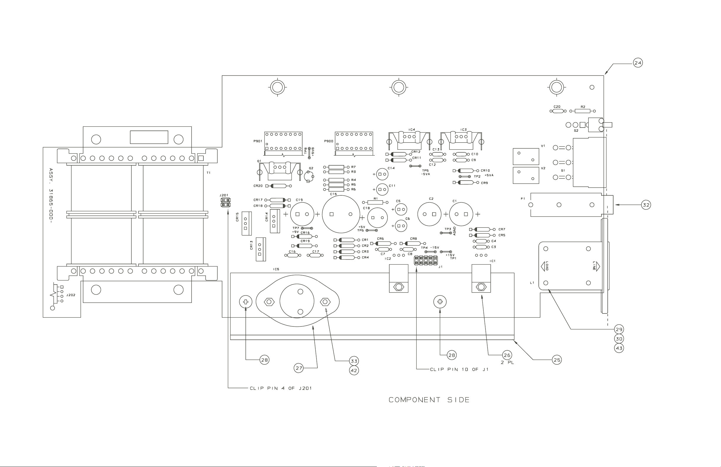
6-78
TECHNICAL DATA Orban Model 2200
Power Supply version 1
Drawing 31865.000.01
Reference schematic 61181.000.01
Page 81
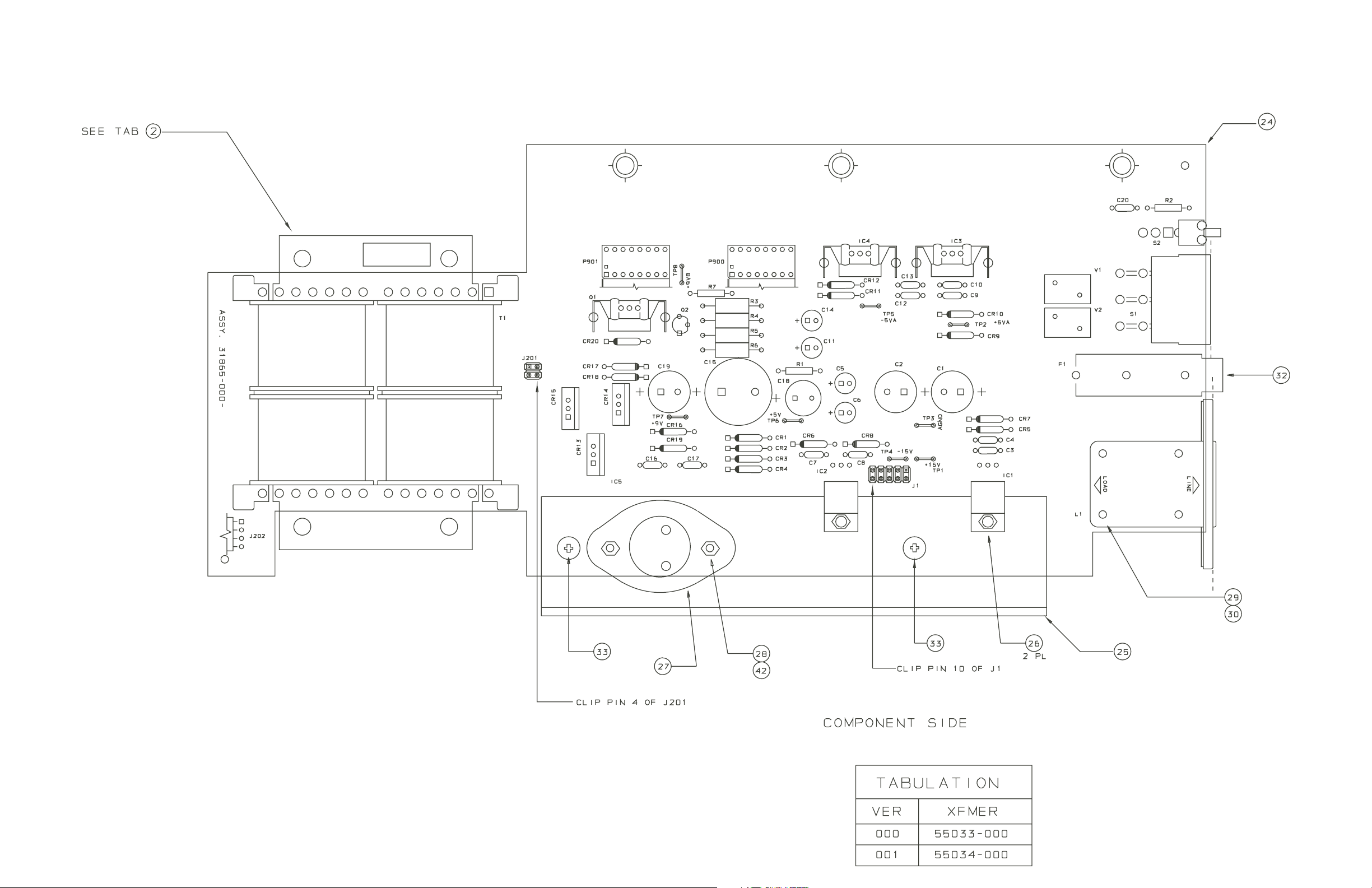
OPTIMOD-FM DIGITAL TECHNICAL DATA
6-79
Power Supply version 2
Drawing 31865-[see tab]-02
Reference schematic 61181.000.02
Page 82
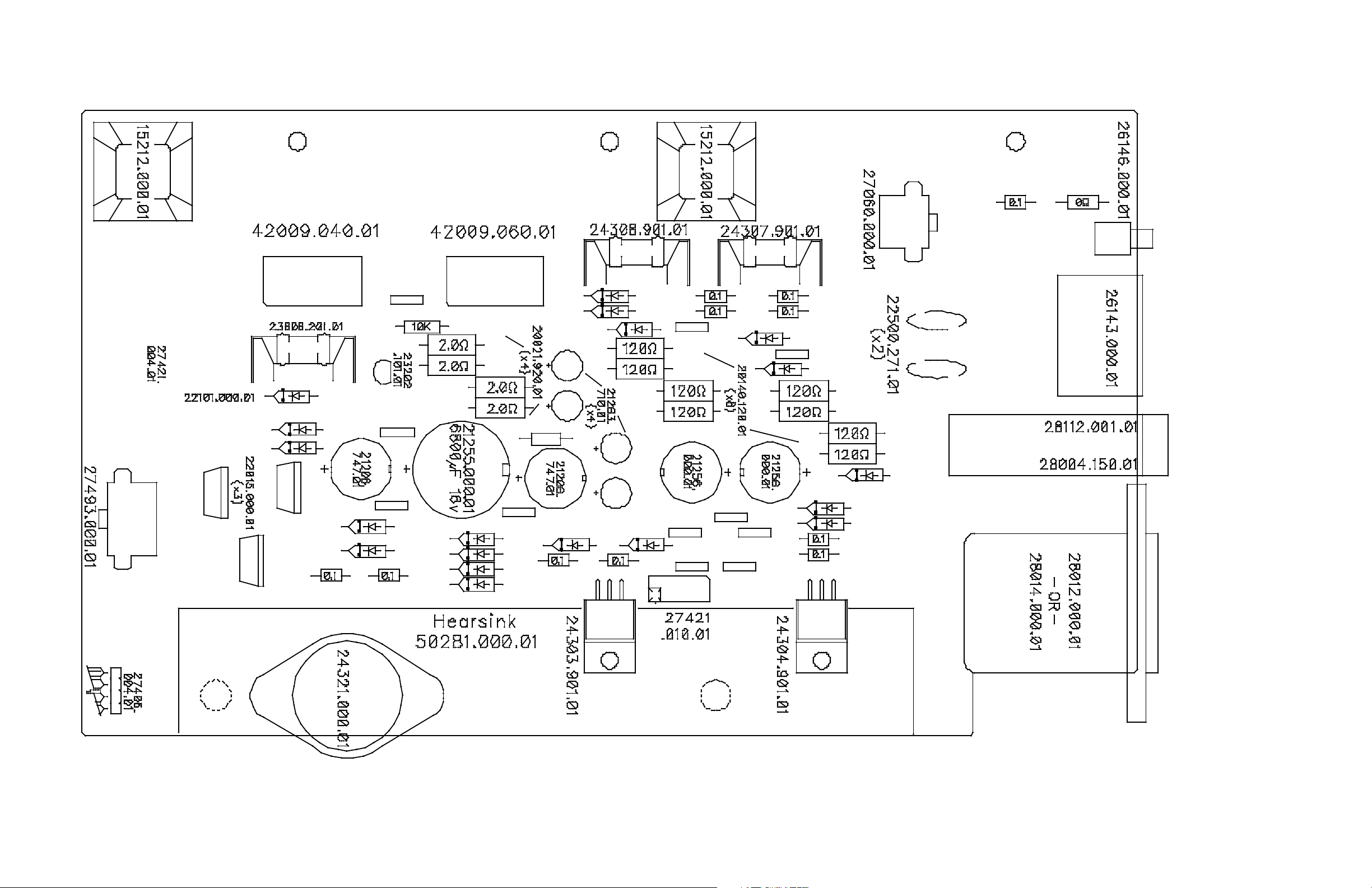
6-80
TECHNICAL DATA Orban Model 2200
Power Supply version 3
Drawing 32045.000.02
Reference schematic 60245.000.03
Page 83
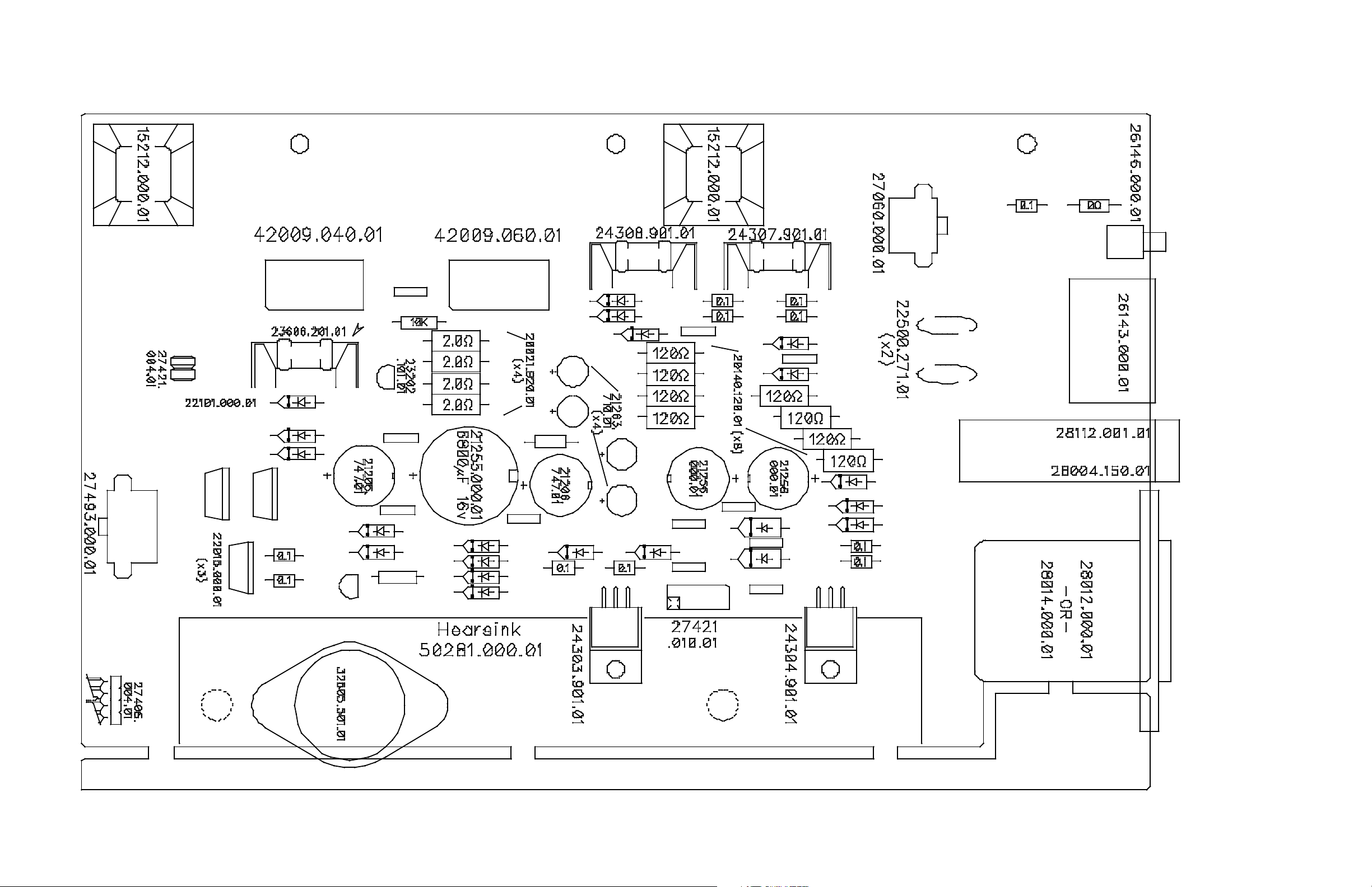
OPTIMOD-FM DIGITAL TECHNICAL DATA
6-81
Power Supply version 4
Drawing 32045.000.05
Reference schematic 60245.000.04
Page 84
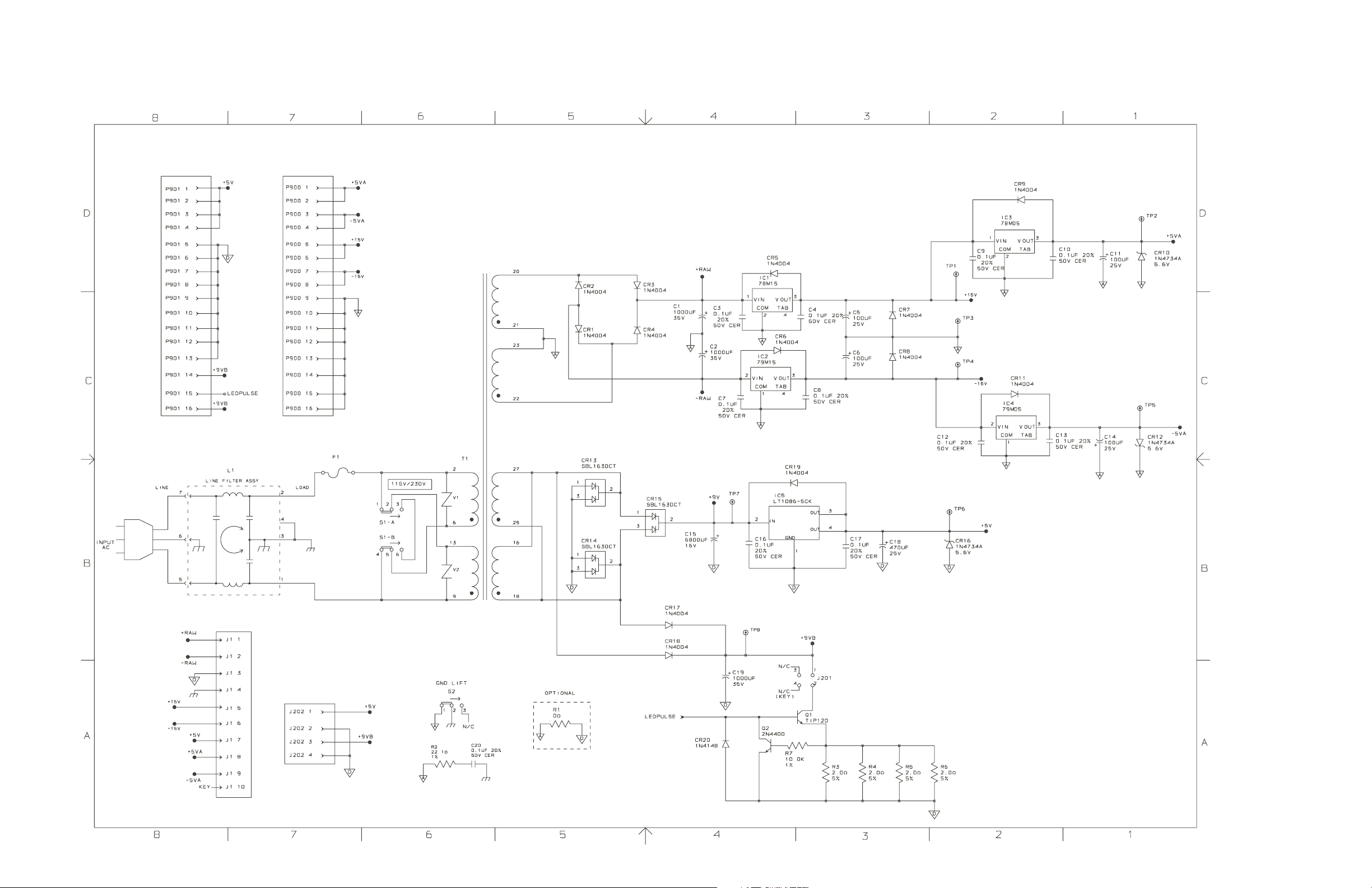
6-82
TECHNICAL DATA Orban Model 2200
Power Supply version 1
Schematic 61181.000.01
Page 85
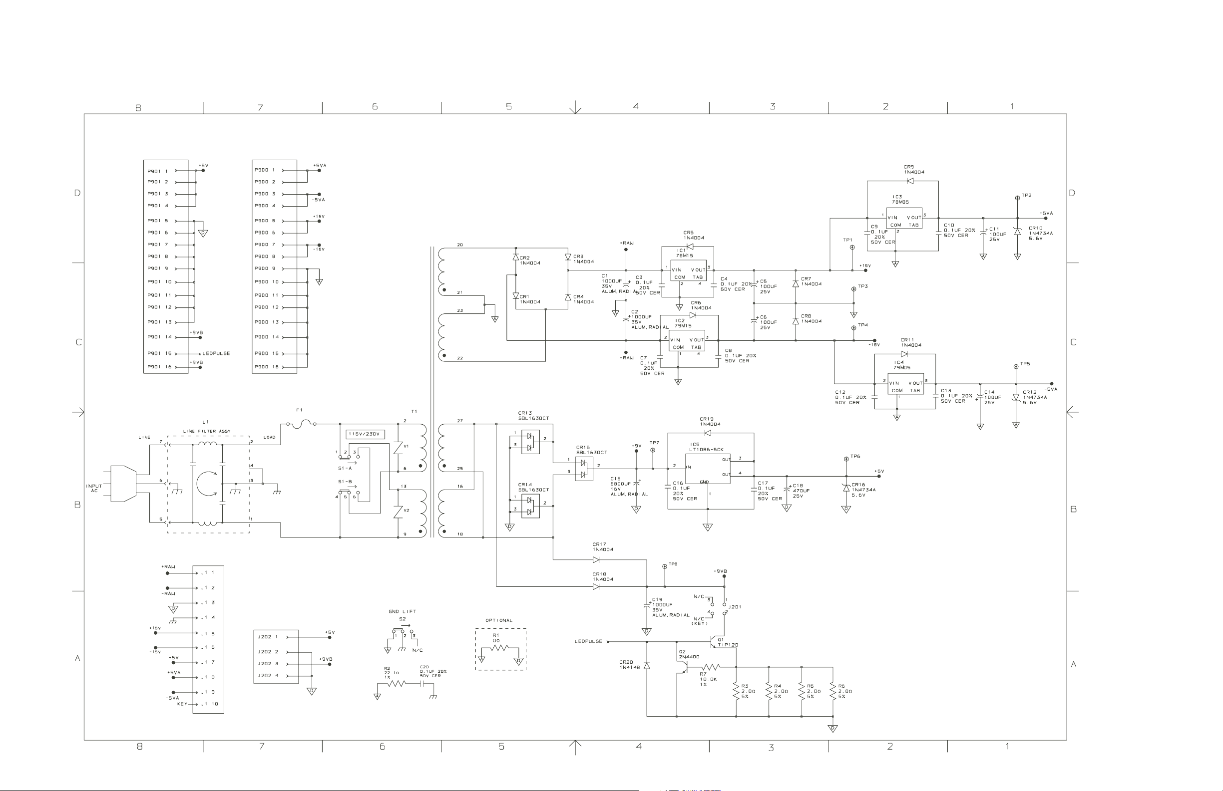
OPTIMOD-FM DIGITAL TECHNICAL DATA
6-83
Power Supply version 2
Schematic 61181.000.02
Page 86
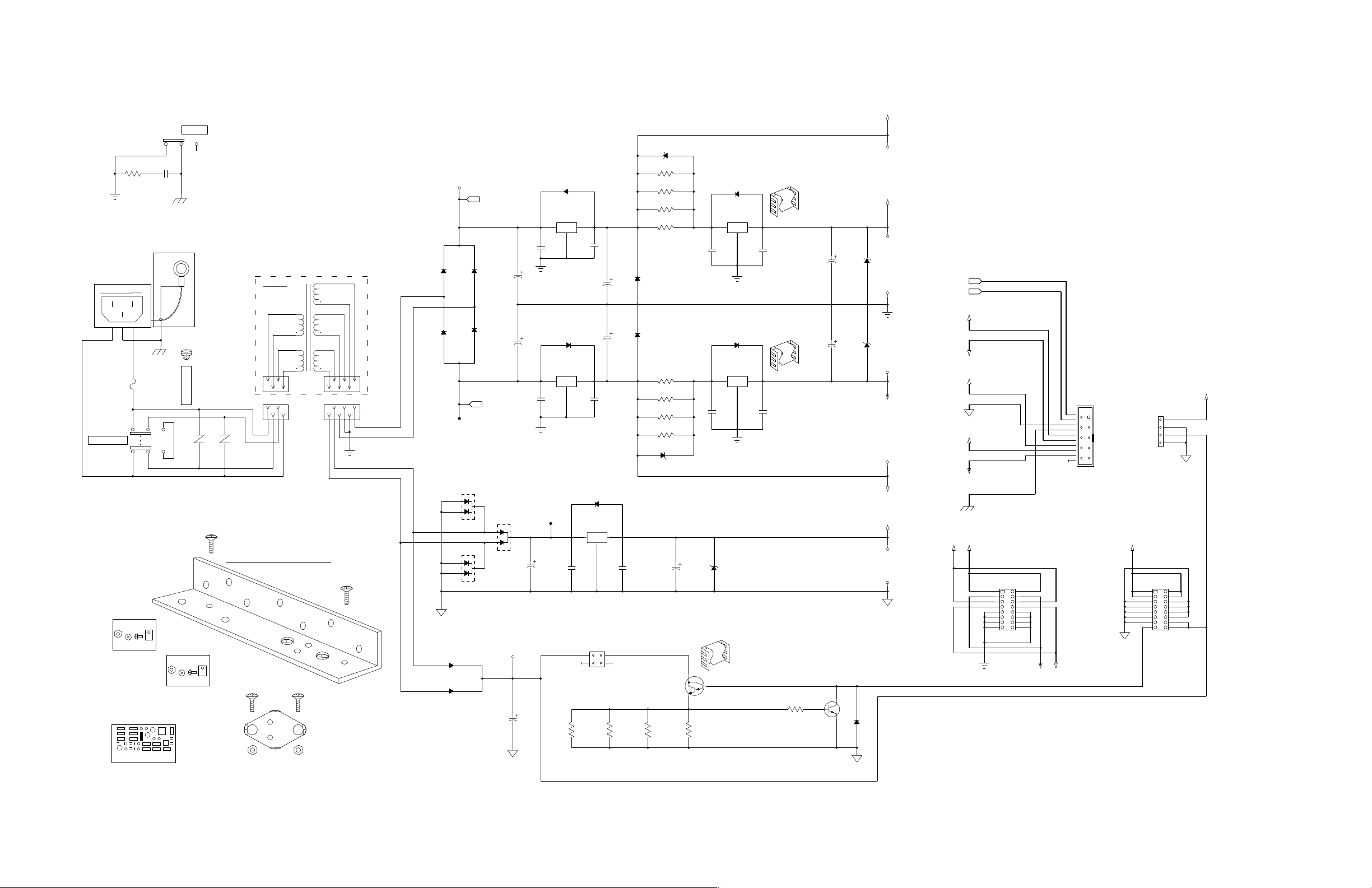
6-84
R2
0W
AGND
L1
Line Filter Assembly
213
1
115v/230v
4
DPDT
S1
IC1
Mounting
Kit
15025.000.01
Ref: PCB
31866.000.05
TECHNICAL DATA Orban Model 2200
+15V
Gnd Lift
1
2
SPDT
S2
0.1F, 50v
C20
1 2
20%
3
N/C
Chassis_Gnd
Chassis Ground Pigtail, 3" long
(Lug w/Green AWG 18)
H13
4
Chassis_Gnd
Cap
F1b
F1a
F1
Fuse
Fuse Holder
1/2 A, Slow Blow Blow
2
3
1 2
5
V1
6
4-40x.3125
IC2
Mounting
Kit
15025.000.01
Power Transformer
Toroid Assy
(off board)
WHITE
BLUE
BROWN
BLACK
4 2 3 1 1 4 2 5 3 6
J4
423
1
1 2
V2
M is c . H ard w are A c c e s s o rie s
Heatsink
50281.000.01
4-40x.375
4-40x.375
IC5
TO3 Insulator
4/40 4/40
RED/WHITE
J6
ORANGE/WHITE
RED
YELLOW/WHITE
ORANGE
12345
YELLOW
AGND
4-40x.3125
6.8v Zener1N4736
21
CR21
21
R8
12
10%
100F, 25v
100F, 25v 10%
1/2 w.
20%0.1F, 50v
2 1
2 1
R9
R10
R11
R12
R13
R15
1N4736
R5
CR7
CR8
120 Ω
120 Ω
120 Ω
120 Ω
1N4004
1N4004
1 2
120 Ω
120 Ω
120 Ω
120 Ω
CR22
5%
2.0 W
5%
5%
5%
5%
6.8v Zener
C18
TIP120
1/2 w.
16013.000.01
21
21
21
5%
21
5%
21
5%
21
5%R14
21
10%
12
470F, 25v
CR9
21
1N4004
+5v Reg
MC78M05CT
1
2
IC3
12
20%
C9
0.1F, 50v
AGND
CR11
2 1
1N4004
-5v Reg
MC79M05CT
2
1
IC4
20%
12
C12
0.1F, 50v
AGND
CR16
2 1
1N4734A
5.6v Zener
3
3
12
C10
12
C13
20%0.1F, 50v
16013.000.01
20%0.1F, 50v
Heatsink
Heatsink
H11
H12
16013.000.01
Heatsink
Q1
3 2
R6
H10
1
LED_Pulse
R7
5%2.0 W
1%10.0K
1/2 w.
TP10
1-2C
PlusRAW
0.1F, 50v
CR4
CR3
2 1
2 1
1N4004
1N4004
12
20%
1000F, 35v
CR1
CR2
2 1
1N4004
1N4004
2 1
12
20%
1000F, 35v
MinusRAW
1-2C
6
TP11
0.1F, 50v
CR13
1
2
3
SBL1630CT
CR14
1
3
CR15
3
+9v
2
1
SBL1630CT
2
12
C15
SBL1630CT
DGND
CR18
2 1
1N4004
CR17
2 1
1N4004
TP8
+9vB
21
C19
20%
1000F, 35v
DGND
CR5
21
1N4004
+15v Reg
MC78M15CT
1
IC1
2
12
C3
20%
AGND
C1
Plus15V
3
12
20%
C4
0.1F, 50v
12
C5
3
12
C8
CR19
1N4004
+5v Reg
LT1086/CK-5
1
2
20%0.1F, 50v
LCD Backlight
J201
1 2
3 4
5%
1/2 w.
2.0 W
12
C6
Minus15V
20%
0.1F, 50v
21
3
IC5
C17
N/CN/C
5%
R4
2.0 W
CR6
C2
2 1
1N4004
-15v Reg
MC79M15CT
2
1
21
IC2
C7
20%
AGND
TP7
20%
21
C16
6800F, 16v
R3
2N4400
Q2
2
Plus15V
TP1
+5VA
Plus5VA
TP2
12
C11
10%
CR10
2 1
100F, 25v
12
C14
100F, 25v
Minus5VA
Minus15V
Power
DGND
1N4734A
5.6v Zener
1-6D
TP3
AGND
10%
CR12
2 1
1N4734A
5.6v Zener
1-6C
TP5
—5VA
TP4
-15V
+5VD
TP6
+15V
TP9
DGND
+15V
-15V
+5VD
DGND
+5VA
—5VA
+5VA
Chassis_Gnd
AGND
PlusRAW
MinusRAW
Plus15V
Minus15V
Power
DGND
Plus5VA
Minus5VA
P900
1 2
3 4
5 6
7 8
9 10
11 12
13 14
15 16
8.5" Flat Cable
—5VA
N/C (Key)
-15V
1
2
3
4
5
6
7
8
9
10
J1
Testing Access
+5VD
Power
1
2
3
4
J202
DGND
Display Supply
+5VD
Digital SupplyAnalog Supply
P901
Power
1 2
3 4
5 6
7 8
9 10
11 12
13 14
15 16
4" Flat Cable
DGND
LED_Pulse
+9vB
1 3
CR20
2 1
1N4148
Power Supply version 3
DGND
schematic 62045.000.03
Page 87
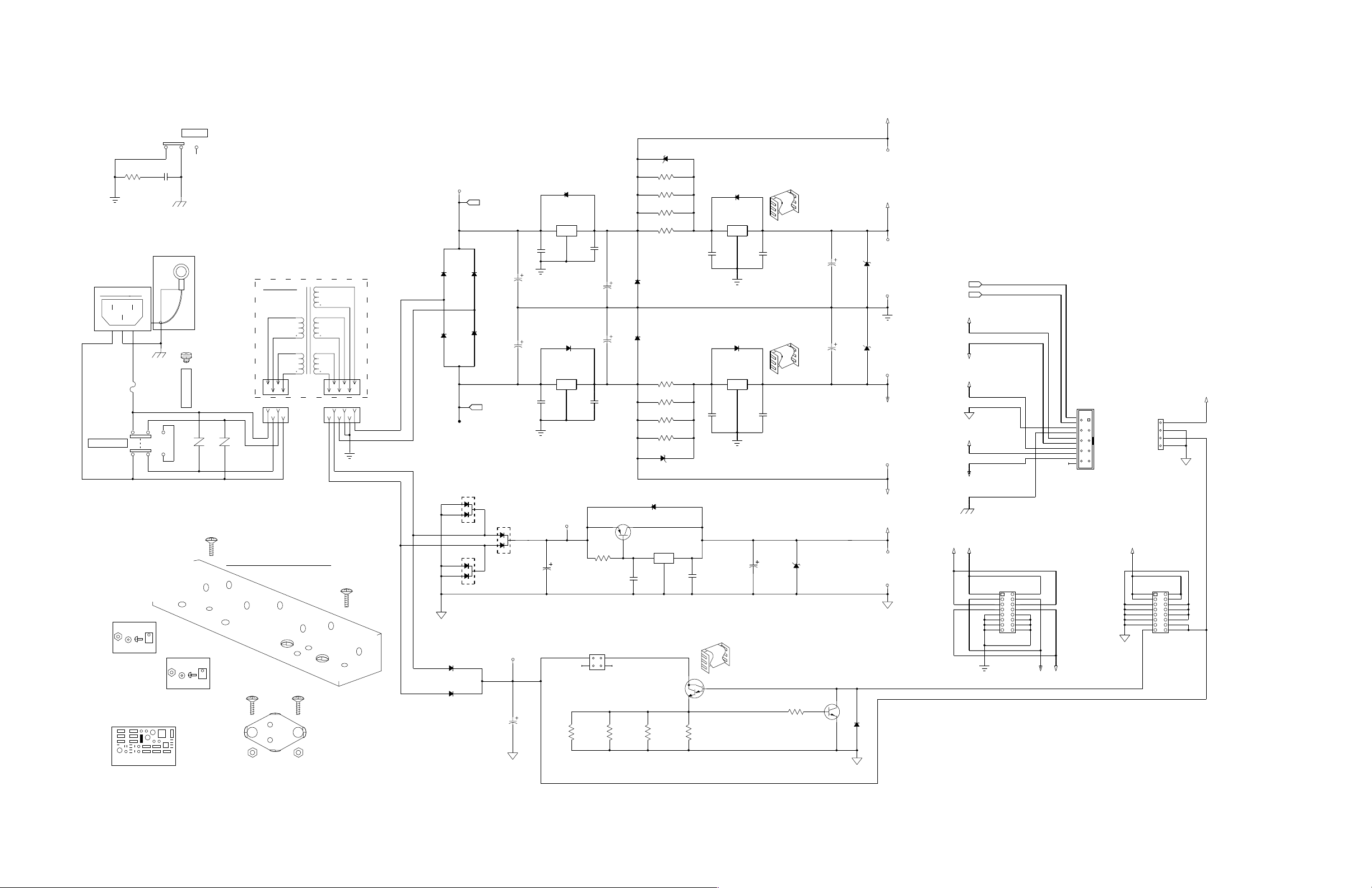
OPTIMOD-FM DIGITAL TECHNICAL DATA
6-85
AGND
Line Filter Assembly
213
115v/230v
DPDT
S1
15025.000.01
SPDT
S2
R2
1 2
0W
0.1F, 50v
Chassis Ground Pigtail, 3" long
(Lug w/Green AWG 18)
L1
4
F1
Fuse
1/2 A, Slow Blow Blow
1
2
4
5
IC1
Mounting
Kit
Ref: PCB
31866.000.05
1
C20
20%
Chassis_Gnd
H13
3
6
Mounting
15025.000.01
2
F1b
F1a
Kit
Gnd Lift
Fuse Holder
V1
IC2
3
N/C
Chassis_Gnd
Cap
1 2
1 2
V2
4-40x.3125
M is c . H ard w are A c c e s s o rie s
Heatsink
50281.000.01
4-40x.375
4/40 4/40
Power Transformer
Toroid Assy
(off board)
WHITE
BLUE
BROWN
BLACK
4 2 3 1 1 4 2 5 3 6
J4
423
1
YELLOW/WHITE
ORANGE/WHITE
ORANGE
RED/WHITE
RED
J6
12345
4-40x.375
IC5
TO3 Insulator
YELLOW
4-40x.3125
+15V
Plus15V
6.8v Zener1N4736
21
CR21
R8
R9
CR7
CR8
R12
R13
R15
1N4736
120 Ω
120 Ω
120 Ω
120 Ω
1N4004
1N4004
1 2
120 Ω
120 Ω
120 Ω
120 Ω
CR22
21
5%
21
5%
21
5%
21
5%
5%
21
5%
21
5%
21
5%R14
21
6.8v Zener
16013.000.01
CR9
21
1N4004
+5v Reg
MC78M05CT
1
2
IC3
12
20%
C9
0.1F, 50v
Heatsink
3
C10
H11
20%0.1F, 50v
12
Plus5VA
12
C11
10%
100F, 25v
AGND
16013.000.01
CR11
2 1
1N4004
-5v Reg
MC79M05CT
2
3
1
IC4
20%
12
C12
0.1F, 50v
AGND
Heatsink
H12
20%0.1F, 50v
12
C13
12
C14
10%
100F, 25v
Minus5VA
0.1F, 50v
C2
0.1F, 50v
CR5
21
1N4004
+15v Reg
MC78M15CT
1
3
IC1
2
12
12
C3
20%
AGND
C1
CR6
2 1
1N4004
-15v Reg
MC79M15CT
2
1
21
IC2
C7
20%
AGND
20%
C4
0.1F, 50v
12
12
C6
3
12
C8
0.1F, 50v
Plus15V
C5
Minus15V
20%
R10
R11
10%
2 1
100F, 25v
2 1
100F, 25v 10%
TP10
1-2C
PlusRAW
CR4
CR3
2 1
2 1
1N4004
1N4004
12
20%
1000F, 35v
CR1
CR2
2 1
1N4004
1N4004
2 1
12
20%
1000F, 35v
MinusRAW
1-2C
6
AGND
TP11
Minus15V
DGND
CR18
2 1
1N4004
CR17
2 1
1N4004
CR13
1
3
SBL1630CT
CR14
1
3
SBL1630CT
2
R16
332 W
1%
MJ2955
2 C
21
CR15
3
+9v
2
1
SBL1630CT
2
TP7
20%
12
C15
6800F, 16v
LCD Backlight
TP8
J201
1 2
3 4
+9vB
21
C19
20%
1000F, 35v
DGND
5%
R3
R4
1/2 w.
2.0 W
CR19
Q3
1
21
1N4004
IC6
+5v Reg.
LP2950-5.0
1
3
2
12
C16
20%
0.1F, 50v
12
20%
C17
0.1F, 50v
12
C18
10%
CR16
2 1
470F, 25v
1N4734A
Power
5.6v Zener
DGND
16013.000.01
N/CN/C
Q1
TIP120
1/2 w.
5%
R5
1/2 w.
2.0 W
5%
2.0 W
Heatsink
H10
1
3 2
5%2.0 W
R6
1/2 w.
LED_Pulse
2N4400
Q2
R7
2
1%10.0K
1 3
CR20
2 1
DGND
CR10
CR12
2 1
2 1
1N4148
+5VA
1N4734A
5.6v Zener
AGND
1N4734A
5.6v Zener
—5VA
-15V
+5VD
DGND
TP1
TP2
1-6D
TP3
1-6C
PlusRAW
MinusRAW
+15V
Plus15V
Minus15V
-15V
TP5
TP4
TP6
TP9
+5VD
Power
DGND
DGND
+5VA
Plus5VA
Minus5VA
—5VA
Chassis_Gnd
+5VA
+15V
P900
1 2
3 4
5 6
7 8
9 10
11 12
13 14
15 16
8.5" Flat Cable
AGND
—5VA
N/C (Key)
-15V
1
2
3
4
5
6
7
8
9
10
J1
Testing Access
1
2
3
4
J202
Display Supply
+5VD
Digital SupplyAnalog Supply
P901
Power
1 2
3 4
5 6
7 8
9 10
11 12
13 14
15 16
4" Flat Cable
DGND
+5VD
Power
DGND
LED_Pulse
+9vB
Power Supply version 4
schematic 62045.000.04
 Loading...