OPTEK OPF562, OPF561, OPF560 Datasheet

Prod uct Bul le tin OPF560
Feb ru ary 1996
125 MHz Fiber Optic Receiver
Types OPF560, OPF561, OPF562
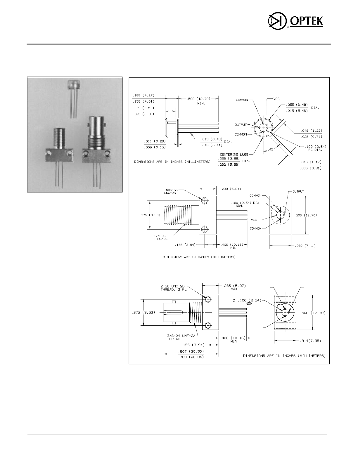
OPF560
V
V
EE
OUTPUT
CC
OPF561
OUTPUT
V
EE
Fea tures
• Low Cost
• Data Rates up to 155 MBd
• Wide Temperature Range
• SMA, ST*, or plastic cap style
• Wave Solderable
V
CC
De scrip tion
The OPF560 series receiver is a low cost
solution for high speed fiber optic
communication designs.
The output of the receiver is an analog,
low impedance, emitter follower voltage
source capable of driving an amplifier or
level translating circuitry. This allows the
subsequent circuitry to use the device in
either the analog mode or translated to
ECL/TTL levels for use in a digital mode
at data rates up to 155MBaud.
The receiver is comprised of a high
speed, low noise, photodiode coupled to
a transimpedance amplifier which
produces an output voltage proportional
to the input light amplitude. This hybrid
approach solves many of the problems of
high speed data link designs by placing a
pre-amplifier close to the photodiode.
The amplification of the transimpedance
amplifier makes the output signal much
less susceptible to EMI.
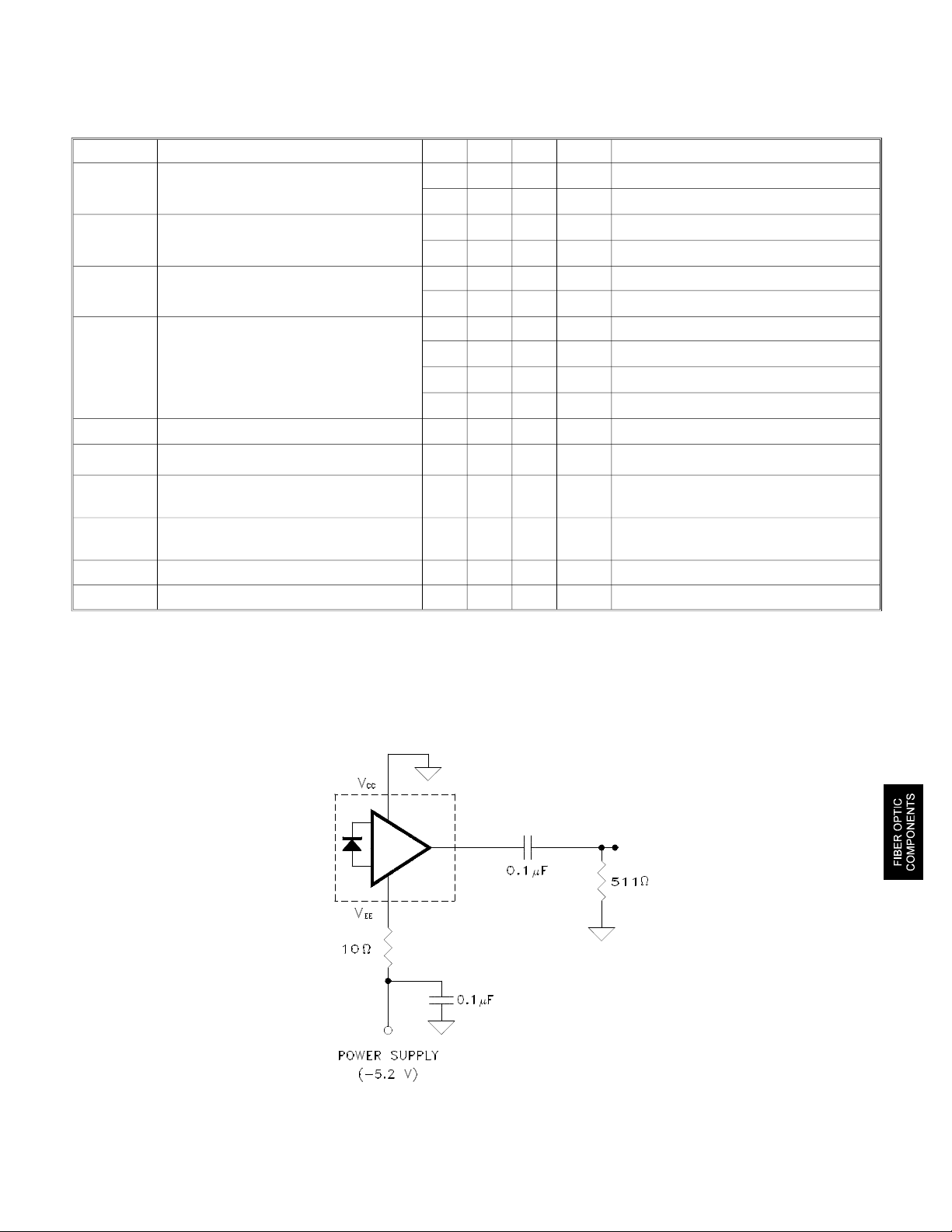
An AC coupled receiver application
circuit is shown. Both the 10 ohm
resistor and by-pass capacitor are
critical.
*ST is a registered trademark of AT&T.
Op tek Tech nol ogy, Inc. 1215 W. Crosby Road Car roll ton, Texas 75006 (972) 323- 2200 Fax (972) 323- 2396
OPF562
OUTPUT
V
CC
V
EE
Ab so lute Maxi mum Rat ings (TA = 25o C un less oth er wise noted)
Stor age Tem pera ture . . . . . . . . . . . . . . . . . . . . . . . . . . . . . . . . . . . . . -55o C to +85o C
Op er at ing Tem pera ture . . . . . . . . . . . . . . . . . . . . . . . . . . . . . . . . . . . -40o C to +85o C
Lead Sol der ing Tem pera ture (for 10 sec.). . . . . . . . . . . . . . . . . . . . . . . . . . . . . 260o C
Sig nal Pin Volt age. . . . . . . . . . . . . . . . . . . . . . . . . . . . . . . . . . . . . . . . . . . . -0.5 to V
Sup ply Volt age (VCC - VEE). . . . . . . . . . . . . . . . . . . . . . . . . . . . . . . . . . . . -0.5 to 6.0 V
Out put Cur rent . . . . . . . . . . . . . . . . . . . . . . . . . . . . . . . . . . . . . . . . . . . . . . . . . . 25 mA
This component is susceptible to damage from electrostatic discharge (ESD). Normal
static precautions should be taken in handling and assembly of this component to
prevent ESD damage or degradation.
8-108
CC

Types OPF560, OPF561, OPF562
Elec tri cal Char ac ter is tics (TA = 25o C un less oth er wise noted)
-5.45 ≤ Sup ply Volt age ≤ -4.75, R
= 511 Ω, Fi ber Sizes ≤ 100 Mi crons, N.A. ≤ 0.35
LOAD
SYM BOL PA RAME TER MIN TYP MAX UNIT TEST CON DI TION
R
P
RMS Output Noise Voltage
V
NO
Responsivity
P
Equivalent Optical Noise Input Power
N
(RMS)
5.3 7 9.6
4.5 11.5
mV/µW
mV/µW at 840 nm, 50 MHz -40o C ≤ TA ≤ +85o C
0.40 0.59 mV
0.7 mV
-43.0 -41.4 dBm Bandwidth Filtered @ 75 MHz
0.050 0.065
Peak Input Power -7.6 dBm TA = 25o C
175
P
R
-8.2 dBm
150
V
odc
I
EE
tr, t
PWD
DC Output Voltage
Power Supply Current
Rise Time, Fall Time
f
(10% to 90%)
Pulse Width Distortion
-4.2 -3.1 -2.4 V
9 15 mA
3.3 6.3 ns
0.4 2.5 ns
BW Bandwidth 125 MHz -3 dB Electrical
PSRR Power Supply Rejection Ratio 20 dB @ 10 MHz
at 840 nm, 50 MHz
Bandwidth Filtered @ 75 MHz, PR = 0 µW
Unfiltered Bandwidth PR = 0 µW
µW
TA = 25o C
µW
-40o C ≤ TA ≤ +85o C
µW -40o C ≤ TA ≤ +85o C
PR = 0 µW
R
= ∞
LOAD
PR = 100 µW, R
C
= 5 pF
LOAD
LOAD
= 511 Ω,
PR = 150 µW Peak, Pwidth = 10 ns,
50% Duty Cycle
Recommended AC Coupled
Receiver Circuit
OUTPUT
8-109
 Loading...