

OPTEK OPB688, OPB687, OPB686, OPB685 Datasheet
Prod uct Bul le tin OPB685
July 1996
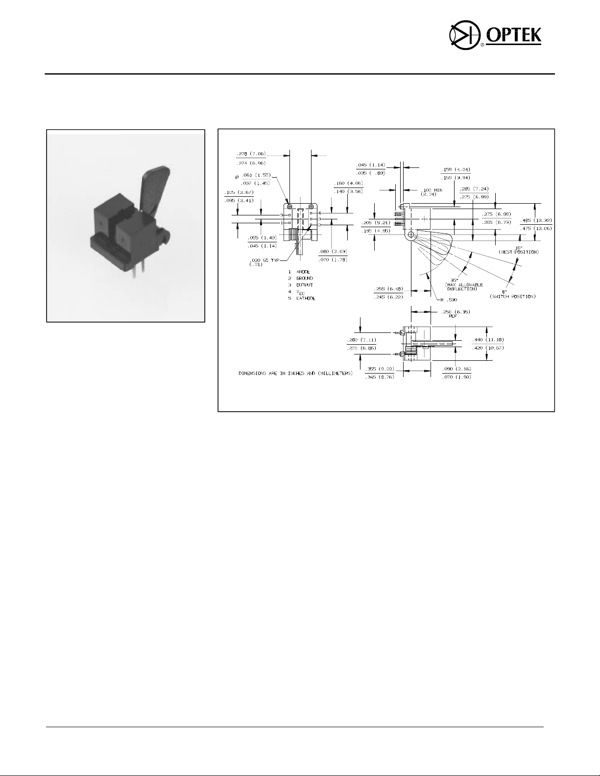
Photologic® Optical Flag Switch
Types OPB685, OPB686, OPB687, OPB688
Fea tures
• Photologic
®
output
• Four output options
• Mechanical switch replacement
• Printed circuit board mounting
De scrip tion
The OPB685 series flag switches consist
of an infrared emitting diode and a
monolithic integrated circuit, which
incorporates a photodiode, a linear
amplifier and a Schmitt trigger. A lever
arm actuated flag interrupts the light
beam switching the output between
states that can readily drive logic gates.
Customized lever arms and spring
torques can be designed for specific
applications.
The device features TTL/LSTTL
compatible logic level output which can
drive up to 10 TTL loads over a voltage
range from 4.5 V to 16 V.
Ab so lute Maxi mum Rat ings (TA = 25o C un less oth er wise noted)
Stor age Tem pera ture Range . . . . . . . . . . . . . . . ...... . . . . . . . . . -40o C to +100o C
Op er at ing Tem pera ture Range . . . . . . . . . . . . . . . . . . . . . . . . . . . . -40o C to +100o C
Lead Sol der ing Tem pera ture [1/16 inch (1.6 mm) from case for 5 sec. with sol der ing
iron] . . . . . . . . . . . . . . . . . . . . . . . . . . . . . . . . . . . . . . . . . . . . . . . . . . . . . . . . . . 240o C
In put Di ode
For ward DC Cur rent. . . . . . . . . . . . . . . . . . . . . . . . . . . . . . . . . . . . . . . . . . . . . . 50 mA
Peak For ward Cur rent (1µs pulse width, 300 pps). . . . . . . . . . . . . . . . . . . . . . . . 3.0 A
Re verse DC Volt age. . . . . . . . . . . . . . . . . . . . . . . . . . . . . . . . . . . . . . . . . . . . . . . 3.0 V
Power Dis si pa tion . . . . . . . . . . . . . . . . . . . . . . . . . . . . . . . . . . . . . . . . . . . . 100 mW
Out put Pho tologic
Sup ply Volt age, VCC. . . . . . . . . . . . . . . . . . . . . . . . . . . . . . . . . . . . . . . . . . . . . . . 18 V
Du ra tion of Out put Short To VCC. . . . . . . . . . . . . . . . . . . . . . . . . . . . . . . . . . . 1.00 sec
Volt age at Out put. . . . . . . . . . . . . . . . . . . . . . . . . . . . . . . . . . . . . . . . . . . . . . . . . . 30 V
Low Level Out put Cur rent (sink ing) . . . . . . . . . . . . . . . . . . . . . . . . . . . . . . . . . . 16 mA
Power Dis si pa tion . . . . . . . . . . . . . . . . . . . . . . . . . . . . . . . . . . . . . . . . . . . . 240 mW
Notes:
(1) RMA flux is rec om mended. Du ra tion can be ex tended to 10 sec. max. when flow sol der ing.
(2) Der ate line arly 1.33 mW/o C above 25o C.
(3) Der ate line arly 2.50 mW/o C above 30o C.
®
(2)
(3)
Op tek Tech nol ogy, Inc. 1215 W. Crosby Road Car roll ton, Texas 75006 (972)323- 2200 Fax (972)323- 2396
12-56
Types OPB685, OPB686, OPB687, OPB688
Elec tri cal Char ac ter is tics (TA = 25o C un less oth er wise noted)
SYM BOL PA RAME TER MIN TYP MAX UNITS TEST CON DI TIONS
In put Di ode
V
I
R
Out put Pho tologic® Sen sor
V
CC
IF(+)
IF(+)/IF(-)
I
CCH
I
CCL
V
OH
I
OH
V
OL
tr, t
t
PLH
t
PHL
Forward Voltage 1.6 V IF = 10 mA
F
Reverse Current 100
µA
Operating D.C. Supply Voltage 4.5 16.0 V
LED Positive-Going Threshold Current 0.1 1.8 10.0 mA VCC = 5.0 V
Hysteresis Ratio 1.05 1.20 1.60 VCC = 5.0 V
High Level Supply Current:
Buffer, 10K Pull-up OPB685
5.0 12.0 mA
Buffer, Open-Collector OPB686
Inverter, 10K Pull-up OPB687
Inverter, Open-Collector OPB688
4.0 12.0 mA
Low Level Supply Current:
Buffer, 10K Pull-up OPB685
5.5 12.0
mA
Buffer, Open-Collector OPB686 4.0 12.0
Inverter, 10K Pull-up OPB687 6.5 12.0
Inverter, Open-Collector OPB688
High Level Output Voltage:
Buffer, 10K Pull-up OPB685
Inverter, 10K Pull-up OPB687
(VCC-1.5)
(VCC-1.5)
5.0 12.0
(5)
(5)
mA
V
V
High Level Output Current:
Buffer, Open-Collector OPB686
Inverter, Open-Collector OPB688
100 µA
100
µA
Low Level Output Voltage:
Buffer, 10K Pull-up OPB685
0.4 V
Buffer, Open-Collector OPB686
Inverter, 10K Pull-up OPB687
Inverter, Open-Collector OPB688
Output Rise Time, Output Fall Time 30 ns
f
0.4 V
Propagation Delay, Low-High
Buffer, 10K Pull-up OPB685
1.0
µs
Buffer, Open-Collector OPB686
Inverter, 10K Pull-up OPB687
Inverter, Open-Collector OPB688
2.0
µs
Propagation Delay, High-Low
Buffer, 10K Pull-up OPB685
2.0
µs
Buffer, Open-Collector OPB686
Inverter, 10K Pull-up OPB687
Inverter, Open-Collector OPB688
1.0
µs
VR = 3.0 V
VCC = 16 V, No Load On Output,
IF = 10 mA
VCC = 16 V, No Load On Output,
IF = 0 mA
VCC = 16 V, No Load On Output,
IF = 0 mA
VCC = 16 V, No Load On Output,
IF = 10 mA
IOH = 100 µA, IF = 10 mA
IOH = 100 µA, IF = 0 mA
(4)
VCC = 16 V, VOH = 30 V, IF = 10 mA
VCC = 16 V, VOH = 30 V, IF = 0 mA
VCC = 4.5 V, IOL = 16 mA, IF = 0 mA
VCC = 4.5 V, IOL = 16 mA, IF = 10 mA
VCC = 5 V, IF = 0 or 10 mA, f = 10 kHz,
D.C. = 50%, RL = 300 Ω
(4)
(4) Nor mal ap pli ca tion would be with light source blocked, simu lated by IF = 0mA.
(5) VOH = VCC-1.5V for VCC = 4.5V to 16V.
Op tek re serves the right to make changes at any time in or der to im prove de sign and to sup ply the best prod uct pos si ble.
Op tek Tech nol ogy, Inc. 1215 W. Crosby Road Car roll ton, Texas 75006 (972)323- 2200 Fax (972)323- 2396
12-57
 Loading...