Prod uct Bul le tin HDC135
Sep tem ber 1996
High Speed Op to cou plers
Types HDC135, HDC136, HDC135B, HDC136B
Fea tures
• High speed
• TTL compatible
• High common mode transient
immunity
• Wide bandwidth
• Open collector output
De scrip tion
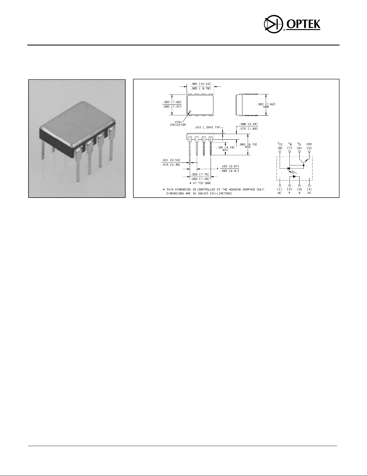
Optek’s HDC135 and HDC136 are high
speed optocouplers, consisting of IR
emitters and integrated photodetectors
in hermetic side brazed dual-in-line 8 pin
packages. Electrical characteristics are
similar to the 6N135 and 6N136
optocouplers but with full military
temperature range operation.
The HDC135B and HDC136B are high
reliability optocouplers with 100%
processing and Group Testing patterned
after MIL-STD-883 Method 5004 and
5005 for class B.
Typical screening and lot acceptance
tests are provided on page 13-4.
Ab so lute Maxi mum Rat ings (No der at ing re quired up to 70o C)
Stor age Tem pera ture Range. . . . . . . . . . . . . . . . ..... . . . . . . . . . -55o C to +150o C
Op er at ing Tem pera ture Range . . . . . . . . . . . . . . . . . . . . . . . . . . . . -55o C to +125o C
Lead Sol der ing Tem pera ture [1/16 inch (1.6 mm) from case for 10 sec onds) . 260o C
Av er age In put Cur rent - IF . . . . . . . . . . . . . . . . . . . . . . . . . . . . . . . . . . . . . . . 25 mA
Peak Out put Cur rent - IF (50% duty cy cle, 1 ms pulse width) . . . . . . . . . . . . 50 mA
Peak Tran sient In put Cur rent - IF (≤ 1 µs pulse width, 300 pps) . . . . . . . . . . . . . 1.0 A
Re verse In put Volt age - VR. . . . . . . . . . . . . . . . . . . . . . . . . . . . . . . . . . . . . . . . . 5.0 V
In put Power Dis si pa tion . . . . . . . . . . . . . . . . . . . . . . . . . . . . . . . . . . . . . . . . 45 mW
Av er age Out put Cur rent - IO . . . . . . . . . . . . . . . . . . . . . . . . . . . . . . . . . . . . . . . 8.0 mA
Peak Out put Cur rent . . . . . . . . . . . . . . . . . . . . . . . . . . . . . . . . . . . . . . . . . . . 16.0 mA
Emitter- Base Re verse Volt age . . . . . . . . . . . . . . . . . . . . . . . . . . . . . . . . . . . . . . 5.0 V
Sup ply and Out put Volt age - VCC, VO . . . . . . . . . . . . . . . . . . . . . . . . . -0.5 V to 15 V
Base Cur rent - IB . . . . . . . . . . . . . . . . . . . . . . . . . . . . . . . . . . . . . . . . . . . . . . . 5.0 mA
Out put Power Dis si pa tion . . . . . . . . . . . . . . . . . . . . . . . . . . . . . . . . . . . . . . 100 mW
Cau tion: This com po nent is sus cep ti ble to dam age from elec tro static dis charge. Nor mal static
pre ven tion pro ce dures should be used in han dling.
Notes:
(1) Der ate line arly above 70o C free- air tem pera ture at a rate of 0.45 mA/o C.
(2) Der ate line arly above 70o C free- air tem pera ture at a rate of 0.9 mA/o C.
(3) Der ate line arly above 70o C free- air tem pera ture at a rate of 0.8 mW/o C.
(4) Der ate line arly above 70o C free- air tem pera ture at a rate of 1.8 mW/o C.
(5) CMH is the maxi mum al low able dV/dt on the lead ing edge of a com mon mode pulse to
as sure that the out put will not switch from high to low.
(6) CML is the maxi mum nega tive dV/dt al low able on the trail ing edge of a com mon mode pulse
to as sure that the out put will not switch from low to high.
(7) Test con di tions rep re sents 1 TTL unit load with 5.6 kΩ pull- up re sis tor.
(8) Test con di tions rep re sents 1 LSTTL unit load with a 6.1 kΩ pull- up re sis tor.
(9) De vice con sid ered a two- terminal de vice: pins 2 and 3 shorted to gether and pins 5, 6, 7 and
8 shorted to gether.
(1)
(2)
(3)
(4)
Minimum orders will apply to processed
devices.
Op tek Tech nol ogy, Inc. 1215 W. Crosby Road Car roll ton, Texas 75006 (214) 323- 2200 Fax (214) 323- 2396
13-22

Types HDC135, HDC136, HDC135B, HDC136B
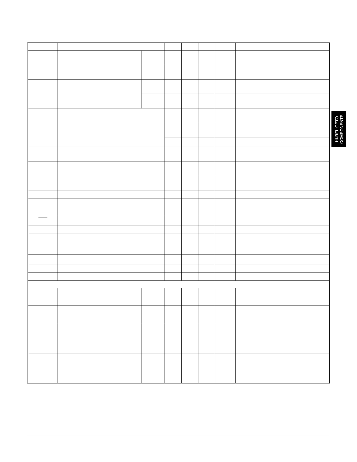
Elec tri cal Char ac ter is tics (Over rec om mended tem pera ture TA = -55o C to +125o C, un less oth er wise noted)
SYM BOL PA RAME TER MIN TYP* MAX UNITS TEST CON DI TIONS
Current Transfer Ratio HDC135
CTR
HDC136
HDC135
HDC136
Logic Low Output Voltage
V
OL
HDC135 0.100 0.40 V
HDC136 0.100 0.40 V
Logic High Output Current
I
OH
I
CCL
Logic Low Supply Current
Logic High Supply Current
I
CCH
V
∆V
∆T
BV
C
Input Forward Voltage 1.50 1.70 V IF = 16 mA, TA = 25o C
F
Temperature Coefficient
F
of Forward Voltage
A
Input Reverse Breakdown Voltage
R
Input Capacitance 42 pF f = 1 MHz, VF = 0
IN
Input-Output Insulation Leakage Current
I
IO
R
C
h
Input-Output Resistance
IO
Input-Output Capacitance 0.50 pF f = 1 MHz (Note 9)
IO
Transistor DC Current Gain 150 — VO = 5 V, IO = 3 mA
FE
Switch ing Speci fi ca tion (TA = 25o C) VCC = 5.0 V, IF = 16.0 mA un less oth er wise noted
t
PHL
t
PLH
Propagation Delay Time
to Logic Low at Output
Propagation Delay Time
to Logic High at Output
Common Mode Transient
CM
Immunity at Logic High
H
Level Output
Common Mode Transient
CM
Immunity at Logic Low
L
Level Output
*
All typicals at TA = 25o C and VCC = 5 V, unless otherwise noted
HDC135
HDC136
HDC135
HDC136
HDC135
HDC136
HDC135
HDC136
7.0
19.0
19.0
25.0
5.0
15.0
15.0
23.0
3.0 500 nA
0.010 1.00
50
40
0.020 1.00
2.0
-1.80 mV/o C
5.0 V
1.00
12
10
0.50
1.50
0.60
1.00
0.40
1.50
0.80
1.00
1000
1000
-1000
-1000
%%IF = 16 mA, VO = 0.40 V,
VCC = 4.5 V, TA = 25o C
%%IF = 16 mA, VO = 0.50 V,
VCC = 4.5 V
IF = 16 mA, IO = 1.10 mA,
VCC = 4.5 V
IF = 16 mA, IO = 2.4 mA,
VCC = 4.5 V
IF = 0 mA, VO = VCC = 5.5 V,
TA = 25o C
IF = 0 mA, VO = VCC = 15 V,
µA
TA = 25o C
IF = 0 mA, VO = VCC = 15 V
µA
IF = 16 mA, VO = open,
µA
VCC = 15 V
IF = 0 mA, VO = open,
µA
VCC = 15 V, TA = 25o C
IF = 0 mA, VO = open,
µA
VCC = 15 V
IF = 16 mA
IR = 10 µA, TA = 25o C
45% Relative Humidity,
t = 5 sec, VIO = 1000 Vdc,
µA
TA = 25o C (Note 9)
VIO = 500 Vdc (Note 9)
Ω
µsµsRL = 4.1 kΩ (Note 8)
RL = 1.90 kΩ (Note 7)
µsµsRL = 4.1 kΩ (Note 8)
RL = 1.90 kΩ (Note 7)
IF = 0 mA, VCM = 10 Vp-p,
V/µs
RL = 4.1 kΩ (Notes 6,8)
IF = 0 mA, VCM = 10 Vp-p,
V/µs
RL = 1.90 kΩ (Notes 6,7)
VCM = 10 Vp-p, RL = 4.1 kΩ,
V/µs
(Notes 5,8)
VCM = 10 Vp-p, RL = 1.90 kΩ
V/µs
(Notes 5,7)
Op tek re serves the right to make changes at any time in or der to im prove de sign and to sup ply the best prod uct pos si ble.
Op tek Tech nol ogy, Inc. 1215 W. Crosby Road Car roll ton, Texas 75006 (214)323- 2200 Fax (214)323- 2396
13-23
 Loading...