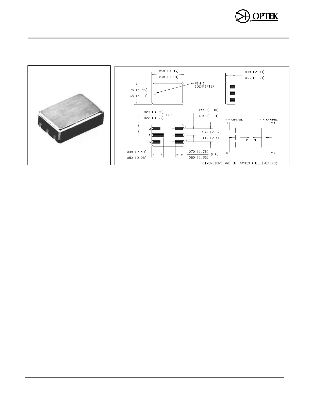
Prod uct Bul le tin HCT802
Sep tem ber 1996
Dual En hance ment Mode MOS FET
Types HCT802, HCT802TX, HCT802TXV
Fea tures
• 6 pad surface mount package
• V
= 90V
DS
• R
• I
• Two devices selected for V
<5Ω
DS(on)
N-Channel = 1.5A
D(on)
P-Channel = 1.1A
and R
DS(on)
similarity
DS
, I
D(on)
• Full TX Processing Available
• Gold plated contacts
De scrip tion
HCT802 offers an N-Channel and PChannel MOS transistor in a hermetic
ceramic surface mount package. The
devices used are similar to industry
standards 2N6661 N-Channel device
and VP1008 P-Channel device. These
two enhancement mode MOSFETS
are particularly well matched for VDS,
I
, R
DS(on)
Order HCT802TX for processing per
MIL-PRF-19500. Typical screening
and lot acceptance tests are provided
on page 13-4. TX products receive a
VGS HTRB at 16 V for 48 hrs. at 150
C and a VDS HTRB at 72 V for 160 hrs.
at 150o C.
DS(on)
and Gfs.
o
Ab so lute Maxi mum Rat ings
Drain- Source Volt age. . . . . . . . . . . . . . . . . . . . . . . . . . . . . . . . . . . . . . . . . . . . . . . 90 V
Gate- Source Volt age. . . . . . . . . . . . . . . . . . . . . . . . . . . . . . . . . . . . . . . . . . . . . . ±20 V
Drain Cur rent (Lim ited by Tj max) N- Channel. . . . . . . . . . . . . . . . . . . . . . . . . . . . . 2 A
P- Channel. . . . . . . . . . . . . . . . . . . . . . . . . . . . 1.1 A
Op er at ing and Stor age Tem pera ture . . . . . . . . . . . . . . . . . . . . . . . . -55o C to +150o C
Power Dis si pa tion
TA = 25o C (Both de vices equally driven) . . . . . . . . . . . . . . . . . . . . . . . . . . 0.5 W To tal
TS = 25o C (Both de vices equally driven). . . . . . . . . . . . . . . . . . . . . . . . . 1.5 W To tal
(Ts = Substrate that the package is soldered to)
Notes
(1) This rating is provided as an aid to designers. It is dependent upon mounting material and
methods and is not measureable as an outgoing test.
(1)
Optek Technology, Inc. 1215 W. Crosby Road Carrollton, Texas 75006 (972) 323-2200 Fax (972) 323-2396
15-34

Types HCT802, HCT802TX, HCT802TXV
Elec tri cal Char ac ter is tics (TA = 25o C un less speci fied oth er wise)
Sym bol Pa rame ters De vice
B=Both
B
VDSS
V
TH
Drain- Source Break down B 90* V ID = 10 µA*, VGS = 0
Gate Thresh old Volt age N 0.75 2.5 V VGS = VDS, ID = 1 mA
P -2.0 -4.5 V ID = -1 mA
I
GSS
I
DSS
Gate- Body Leak age B ±100 nA VGS = ± 20 V, VDS = 0
Zero Gate Volt age Drain Cur rent B 10* µA VDS = 90 V*, VGS = 0 V
B 500* µA Tj = 150o C
I
D(on)
On- State Drain Cur rent N 1.5 A VDS = 25 V, VGS = 10 V
P -1.1 A VDS = -15 V, VGS = -10 V
R
DS(on)
G
fs
Drain- Source on Re sis tance B 5 Ω VGS = 10 V*, ID = 1 A*
For ward Trans con duc tance N 170 mmho VDS = 25 V, ID = 0.5 A
P 200 mmho VDS = -10 V, ID = -0.5 A
C
ISS
In put Ca paci tance N 70 pf V
P 150 pf VDS = -25 V, VGS = 0 V, f = 1 MHz
C
OSS
Com mon Source Out put Ca paci tance
N 40 pf VDS = 25 V, V
P 60 pf VDS = -25 V, VGS = 0 V, f = 1 MHz
Min Max Units Test Con di tions
= 25 V, VGS = 0 V, f = 1 MHz
DS
= 0 V, f = 1 MHz
GS
C
t
(on)
t
(off)
RSS
Re verse Trans fer Ca paci tance N 10 pf VDS = 25 V, VGS = 0 A, f = 1 MHz
Turn- on- time N 15 ns V
Turn- off- time N 17 ns V
* Re verse po lar ity for P- Channel de vice
P 25 pf VDS = -25 V, V
= 25 V, ID = 1 A, RL = 50 Ω
DD
= 0 A, f = 1 MHz
GS
P 50 ns VDD = -25 V, ID = -0.5 A, RL = 50 Ω
= 25 V, ID = 1 A, RL = 50 Ω
DD
P 50 ns VDD = -25 V, ID = -0.5 A, RL = 50 Ω
Op tek re serves the right to make changes at any time in or der to im prove de sign and to sup ply the best prod uct pos si ble.
Op tek Tech nol ogy, Inc. 1215 W. Crosby Road Car roll ton, Texas 75006 (972)323- 2200 Fax (972)323- 2396
15- 35
 Loading...