

Page 1

OP5330 USER GUIDE
Digital to Analog Converter
Module
www.opal-rt.com
Page 2

Published by
OPAL-RT Technologies, Inc. 1751 Richardson, suite 2525 Montréal (Québec) Canada H3K 1G6
www.opal-rt.com
© 2014 OPAL-RT Technologies, Inc. All rights reserved
Printed in Canada
Page 3

CONTENTS
GETTING STARTED ................................................................................................................................ 4
SOFTWARE REQUIREMENTS ............................................................................................................ 4
HARDWARE REQUIREMENTS ........................................................................................................... 4
FEATURES ........................................................................................................................................... 4
INTRODUCTION ..................................................................................................................................... 5
DESCRIPTION .................................................................................................................................... 5
OFFSET AND GAIN CALIBRATION ..................................................................................................................5
MODULE INSTALLATION AND CONFIGURATION .............................................................................. 6
CIRCUIT LAYOUT DIAGRAMS ............................................................................................................. 6
SCHEMATICS ....................................................................................................................................... 7
OP5330 DB37F PIN ASSIGNMENTS .................................................................................................. 8
SPECIFICATIONS ................................................................................................................................... 9
TYPICAL APPLICATIONS .................................................................................................................. 10
3 OPAL-RT Technologies OP5330 User Guide
Page 4

GETTING STARTED
Features
GETTING STARTED
Before you begin, verify that your system meets the requirements of the OP5330 board:
SOFTWARE REQUIREMENTS
• RT-LAB 8.4.0 and higher
• MATLAB 32 bits 6.5 and higher
• Windows XP and higher
HARDWARE REQUIREMENTS
• OP4500 Simulator
• OP5600 HIL simulator
• OP5600 I/O Expansion Unit
• OP5607 I/O Expansion Unit
• OP7000 Expansion Unit with OP7220 Type A Carrier
FEATURES
• HYPERSIM compatible
• 16 single-ended analog output channels
• All outputs are sampled simultaneously, up to 1 MS/s
• 16 bit resolution
• ±16 V voltage range output
• ±15 mA maximum current per channel
• Factory calibrated
OP5330 User Guide OPAL-RT Technologies 4
Page 5

INTRODUCTION
DESCRIPTION
INTRODUCTION
DESCRIPTION
The OP5330 digital to analog converter (DAC) provides 16 single-ended digital output channels. Each
channel uses a 16-bit resolution digital-to-analog converter.
The OP5330 is a part of the OP5000 series of optional modules for OPAL-RT’s state of the art HIL
(hardware-in-the-loop) systems, intended for use with OPAL-RT carrier boards (see “Hardware
Requirements” on previous page). Designed for OPAL-RT’s simulation systems, the OP5330 converts
digital signals to analog.
Each OP5330 can sample up to 1 MS/s, giving a total throughput of 8 MS/s, all channels are
simultaneously sampled. The onboard EEPROM provides offset and gain data adjustment written
during the calibration process, as well as over-voltage protection.
By default, the maximum output signal is set to ±16 volts.
OFFSET AND GAIN CALIBRATION
The OP5330 contains a serial EEPROM to store the module identification, calibration information and
other important information. Each OP5330 is factory calibrated after assembly; during calibration, gain
and offset are adjusted to ensure accurate target output values at ±20 mV noise and offset.
5 OPAL-RT Technologies OP5330 User Guide
Page 6
Module Installation and configuration
Circuit Layout Diagrams
MODULE INSTALLATION AND CONFIGURATION
The OP5330 digital to analog converter must be inserted into the OPAL-RT carrier
OP5330 connector
board using great care. Two polarized connectors fasten the module in the suitable
position and four screws affix it for a more secure connection to the carrier.
Make sure that the connectors are properly aligned; they should fit together easily.
Use light pressure to push the OP5330 board into the carrier board.
The OP5330 module can only be used with OPAL-RT’s carrier boards. Its location
Carrier board connector
and identification on the carrier board are determined by the FPGA controller
bitstream.
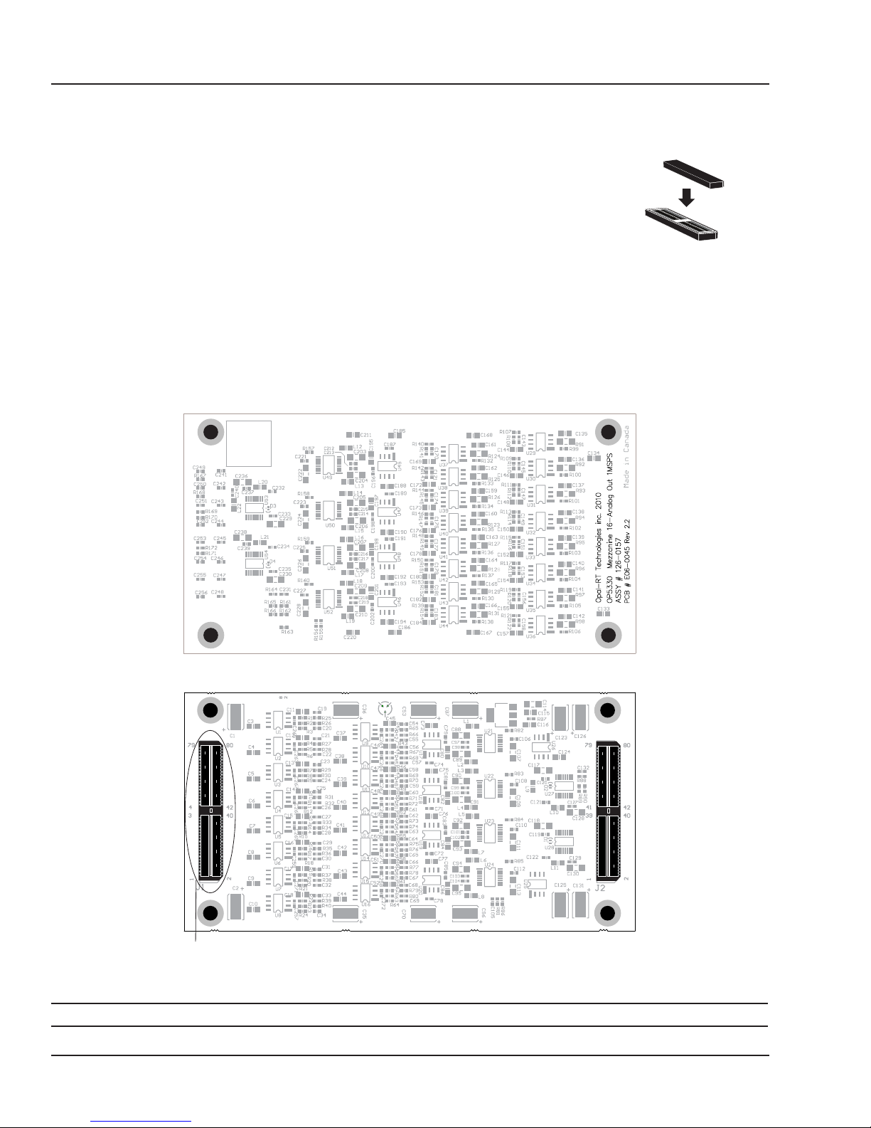
CIRCUIT LAYOUT DIAGRAMS
When the OP5330 is installed on the carrier board, only the top of the circuit board is visible, as shown
in Figure 1. The connectors are located on the bottom of the board (see Figure 2) and fit snugly into the
connectors on the carrier.
Figure 1: OP5330 module (top view)
Connector
Figure 2: OP5330 module (bottom view)
NOTE:
OP5330 User Guide OPAL-RT Technologies 6
Images shown represent revision 2.2 of the board. Versions may vary according to your board.
Page 7
Module Installation and configuration
-
+
SIGNAL DATA
GAIN DATA
OFFSET DATA
GAIN DAC
OUTPUT
VREF SIGNAL DAC
-
+
OFFSET DAC
STAGE 1
STAGE 2
STAGE 3
Schematics
SCHEMATICS
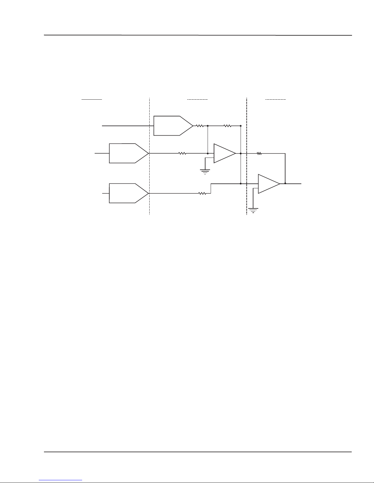
Figure 3 represents a simplified schematic of one channel of the OP5330 module. It is composed of
three stages: the first stage consists of one gain DAC and one offset DAC; the second stage consists of
a signal DAC with an operational amplifier that allows for gain adjustments; the third stage consists of
an operational amplifier that receives final signal value and integrates the offset.
Figure 3: Output DAC circuit
7 OPAL-RT Technologies OP5330 User Guide
Page 8
Module Installation and configuration
OP5330 DB37F Pin Assignments
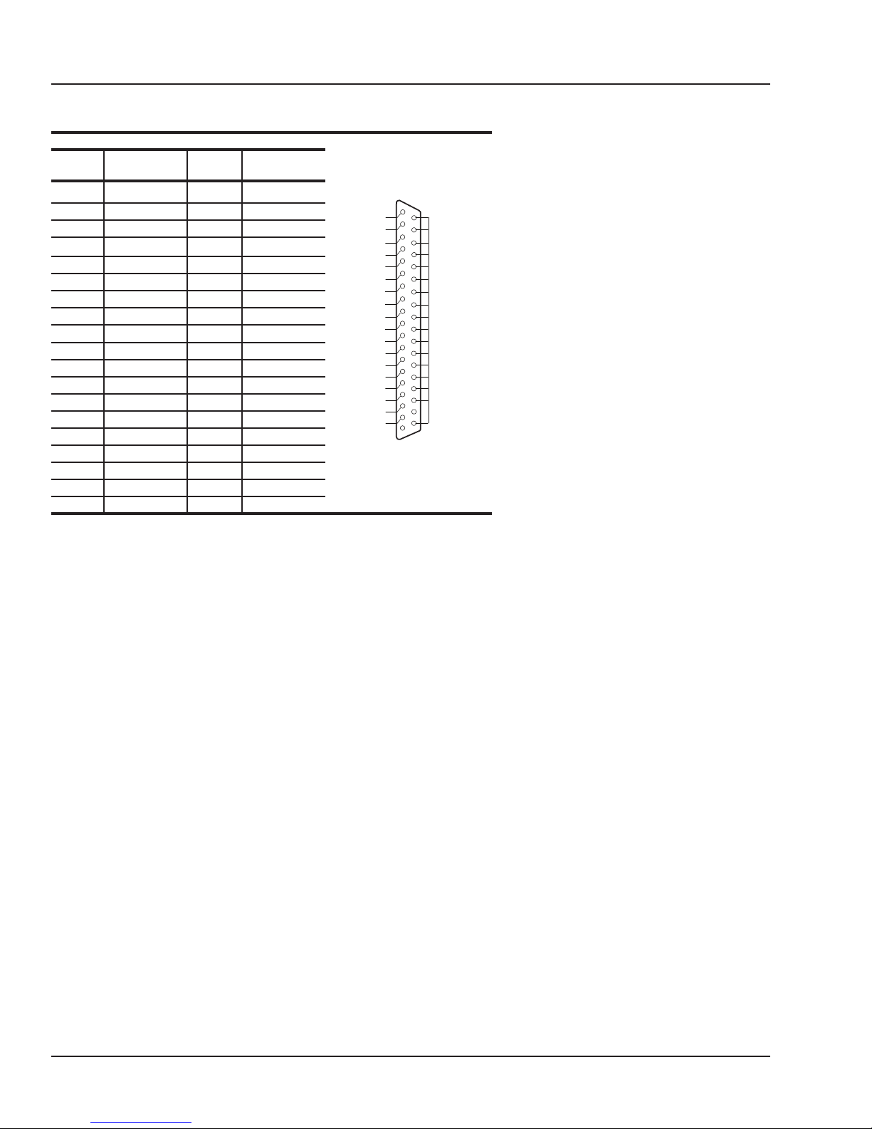
OP5330 DB37F PIN ASSIGNMENTS
Connector P1 Ch. 0-15
DB37F
OP5330 pin
assignment
DB37F
1 +OUT00 20 -GND00
2 +OUT01 21 -GND01
3 +OUT02 22 -GND02
4 +OUT03 23 -GND03
5 +OUT04 24 -GND04
6 +OUT05 25 -GND05
7 +OUT06 26 -GND06
7 +OUT07 27 -GND07
9 +OUT08 28 -GND08
10 +OUT09 29 -GND09
11 +OUT10 30 -GND10
12 +OUT11 31 -GND11
13 +OUT12 32 -GND12
14 +OUT13 33 -GND13
15 +OUT14 34 -GND14
16 +OUT15 35 -GND15
17 36 Standard OPAL-RT
18 Reserved 37 Reserved Simulator DB37 connector
19
OP5330 pin
assignment
00+
01+
02+
03+
04+
05+
06+
07+
08+
09+
10+
11+
12+
13+
14+
15+
Vuser
1
20
-00
-01
-02
-03
-04
-05
-06
-07
-08
-09
-10
-11
-12
-13
-14
-15
Vrtn
37
19
OP5330 User Guide OPAL-RT Technologies 8
Page 9

Specifications
OP5330 DB37F Pin Assignments
SPECIFICATIONS
Product Name: OP5330
Part Number: 126-0157
Number of channels: 16 single-ended
Resolution: 16 bits
Default range: ± 16 Volts
Maximum current: 15 mA
Max. Sampling Frequency: 1 MS/s
Min Conversion / Acquisition Time: 1 μs per channel
DAC Type: 8 x Dual DAC with 10 MBit/s Serial Output Transfer
Dc Transfer Characteristics
CMRR: 100 dB
Dynamic Characteristics
Calibration: Programmable gain and offset calibration for each D/A. Calibration factors are
stored in on-board non-volatile memory (EEPROM)
Maximum noise: 20 mV peak-to-peak
Maximum offset: ± 80 mV
Recommended warm-up time: 5 min.
Calibration interval: as required
Dimensions: 6.60 cm x 12.50 cm (2.6” x 4.92”)
I/O connector: 80-pin high speed header to carrier
Environmental
Operating temperature: 10 to 40 °C
Storage temperature: -55 to 85 °C
Relative humidity: 10 to 90%, non condensing
Maximum altitude: 2,000 m
9 OPAL-RT Technologies OP5330 User Guide
Page 10
Specifications
Typical Applications
TYPICAL APPLICATIONS
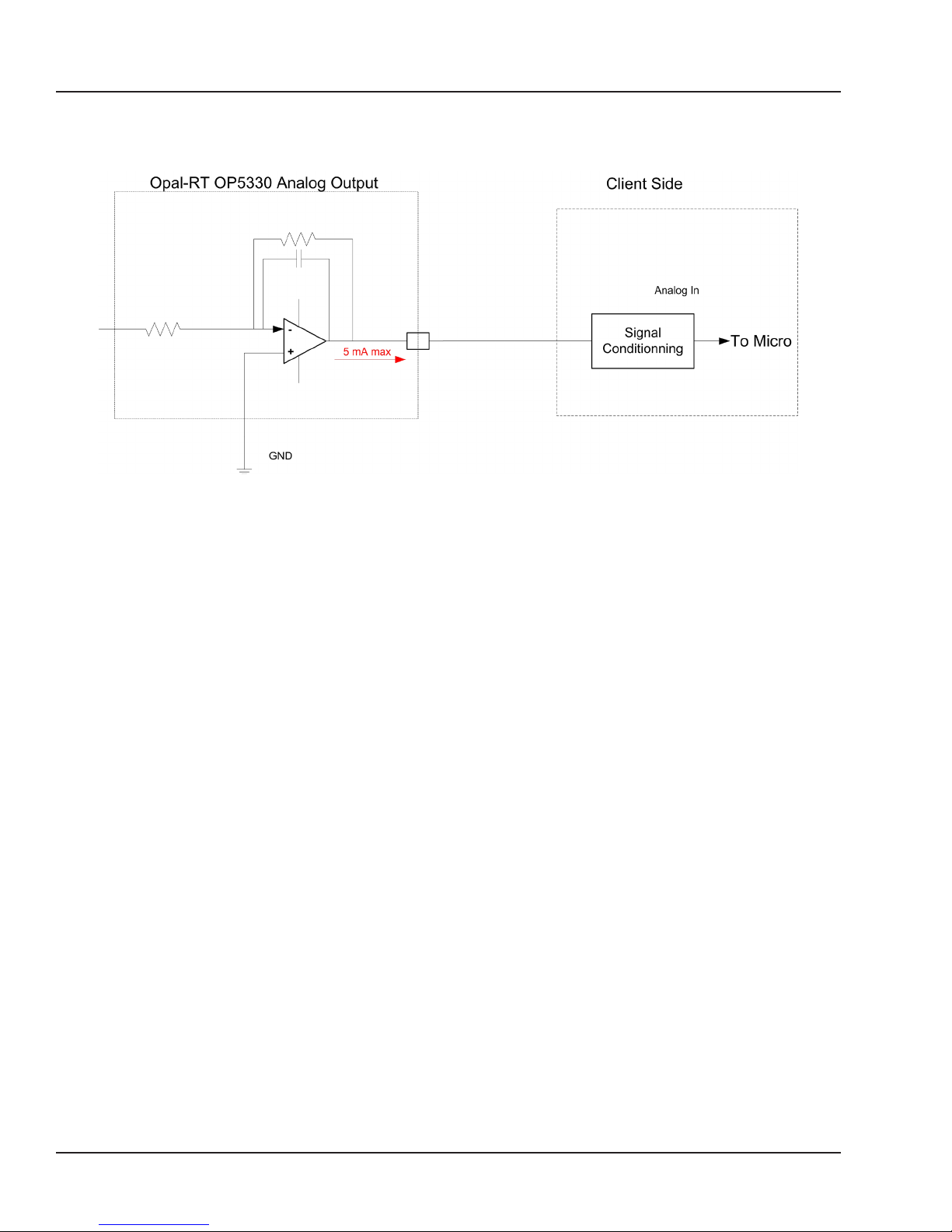
The following diagrams provide an example of a typical application using the OP5330.
OP5330 User Guide OPAL-RT Technologies 10
Page 11

11 OPAL-RT Technologies OP5330 User Guide
Page 12

CONTACT
OPAL-RT Corporate Headquarters
1751 Richardson, Suite 2525
Montréal, Québec, Canada
H3K 1G6
Tel.: 514-935-2323
Toll free: 1-877-935-2323
Technical Services
www.opal-rt.com/support
Note:
While every effort has been made to ensure
accuracy in this publication, no responsibility
can be accepted for errors or omissions. Data
may change, as well as legislation, and you are
strongly advised to obtain copies of the most
recently issued regulations, standards, and
guidelines.
This publication is not intended to form the
basis of a contract.
UG14-18121-OP1
05/2014
© OPAL-RT Technologies Inc.
 Loading...