

TIP140, TIP141, TIP142,
(NPN); TIP145, TIP146,
TIP147, (PNP)
TIP141, TIP142, TIP146, and TIP147 are Preferred Devices
Darlington Complementary
Silicon Power Transistors
Designed for general−purpose amplifier and low frequency
switching applications.
Features
• High DC Current Gain −
Min hFE= 1000 @ IC
= 5.0 A, VCE = 4 V
• Collector−Emitter Sustaining Voltage − @ 30 mA
V
CEO(sus)
• Monolithic Construction with Built−In Base−Emitter Shunt Resistor
• Pb−Free Packages are Available*
= 60 Vdc (Min) − TIP140, TIP145
= 80 Vdc (Min) − TIP141, TIP146
= 100 Vdc (Min) − TIP142, TIP147
http://onsemi.com
10 AMPERE
DARLINGTON
COMPLEMENTARY SILICON
POWER TRANSISTORS
60−100 VOLTS, 125 WATTS
MAXIMUM RATINGS
Rating Symbol
Collector − Emitter Voltage V
Collector − Base Voltage V
Emitter − Base Voltage V
Collector Current
− Continuous
− Peak (Note 1)
Base Current − Continuous I
Total Power Dissipation
@ TC = 25_C
Operating and St orage
Junction Temperature Range
TJ, T
CEO
CB
EB
I
C
B
P
TIP140
TIP145
D
stg
TIP141
TIP146
60 80 100 Vdc
60 80 100 Vdc
−65 to +150
TIP142
TIP147
5.0 Vdc
10
15
0.5 Adc
125 W
Unit
Adc
_C
THERMAL CHARACTERISTICS
Characteristic Symbol Max Unit
Thermal Resistance,
Junction−to−Case
Thermal Resistance,
Junction−to−Ambient
Maximum ratings are those values beyond which device damage can occur.
Maximum ratings applied to the device are individual stress limit values (not
normal operating conditions) and are not valid simultaneously. If these limits are
exceeded, device functional operation is not implied, damage may occur and
reliability may be affected.
1. 5 ms, v 10% Duty Cycle.
R
q
JC
R
q
JA
1.0 °C/W
35.7 °C/W
SOT−93 (TO−218)
CASE 340D
STYLE 1
MARKING DIAGRAM
AYWWG
TIP14x
A = Assembly Location
Y = Year
WW = Work Week
TIP14x = Device Code
x = 0, 1, 2, 5, 6, or 7
G = Pb−Free Package
ORDERING INFORMATION
See detailed ordering and shipping information in the package
dimensions section on page 2 of this data sheet.
*For additional information on our Pb−Free strategy and soldering details, please
download the ON Semiconductor Soldering and Mounting Techniques
Reference Manual, SOLDERRM/D.
© Semiconductor Components Industries, LLC, 2005
September, 2005 − Rev. 5
1 Publication Order Number:
Preferred devices are recommended choices for future use
and best overall value.
TIP140/D
TIP140, TIP141, TIP142, (NPN); TIP145, TIP146, TIP147, (PNP)
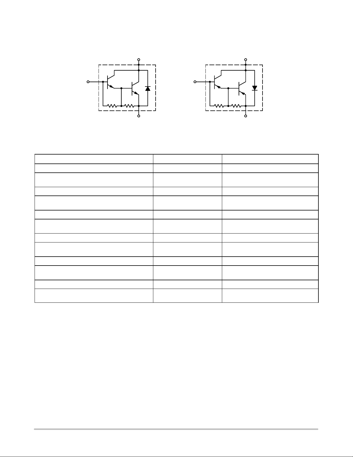
DARLINGTON SCHEMATICS
NPN
TIP140
TIP141
TIP142
BASE
COLLECTOR
≈ 8.0 k ≈ 40
EMITTER
PNP
TIP145
TIP146
TIP147
BASE
COLLECTOR
≈ 8.0 k ≈ 40
EMITTER
ORDERING INFORMATION
Device Package Shipping
TIP140 SOT−93 (TO−218) 30 Units / Rail
TIP140G SOT−93 (TO−218)
(Pb−Free)
TIP141 SOT−93 (TO−218) 30 Units / Rail
TIP141G SOT−93 (TO−218)
(Pb−Free)
TIP142 SOT−93 (TO−218) 30 Units / Rail
TIP142G SOT−93 (TO−218)
(Pb−Free)
TIP145 SOT−93 (TO−218) 30 Units / Rail
TIP145G SOT−93 (TO−218)
(Pb−Free)
TIP146 SOT−93 (TO−218) 30 Units / Rail
TIP146G SOT−93 (TO−218)
(Pb−Free)
TIP147 SOT−93 (TO−218) 30 Units / Rail
TIP147G SOT−93 (TO−218)
(Pb−Free)
30 Units / Rail
30 Units / Rail
30 Units / Rail
30 Units / Rail
30 Units / Rail
30 Units / Rail
http://onsemi.com
2
TIP140, TIP141, TIP142, (NPN); TIP145, TIP146, TIP147, (PNP)
Î
Î
Î
Î
Î
Î
Î
Î
Î
Î
Î
Î
Î
Î
Î
Î
Î
Î
Î
Î
Î
Î
Î
Î
Î
Î
Î
Î
Î
Î
Î
Î
Î
Î
Î
Î
Î
Î
Î
Î
Î
Î
Î
Î
Î
Î
Î
Î
Î
Î
Î
Î
Î
Î
Î
Î
Î
Î
Î
Î
Î
Î
Î
Î
Î
Î
Î
Î
Î
ELECTRICAL CHARACTERISTICS (T
= 25_C unless otherwise noted)
C
Characteristic
OFF CHARACTERISTICS
Collector−Emitter Sustaining Voltage (Note 2)
= 30 mA, IB = 0) TIP140, TIP145
(I
C
ООООООООООООООООО
ООООООООООООООООО
TIP141, TIP146
TIP142, TIP147
Collector Cutoff Current
(VCE = 30 Vdc, IB = 0) TIP140, TIP145
ООООООООООООООООО
(VCE = 40 Vdc, IB = 0) TIP141, TIP146
ООООООООООООООООО
(VCE = 50 Vdc, IB = 0) TIP142, TIP147
Collector Cutoff Current
ООООООООООООООООО
(VCB = 60 V, IE = 0) TIP140, TIP145
(VCB = 80 V, IE = 0) TIP141, TIP146
ООООООООООООООООО
(VCB = 100 V, IE = 0) TIP142, TIP147
Emitter Cutoff Current (VBE = 5.0 V)
ON CHARACTERISTICS (Note 2)
DC Current Gain
ООООООООООООООООО
(IC = 5.0 A, VCE = 4.0 V)
(IC = 10 A, VCE = 4.0 V)
ООООООООООООООООО
Collector−Emitter Saturation Voltage
(IC = 5.0 A, IB = 10 mA)
ООООООООООООООООО
(IC = 10 A, IB = 40 mA)
Base−Emitter Saturation Voltage
(IC = 10 A, IB = 40 mA)
ООООООООООООООООО
Base−Emitter On Voltage
(IC = 10 A, VCE = 4.0 Vdc)
ООООООООООООООООО
SWITCHING CHARACTERISTICS
Resistive Load (See Figure 1)
Delay Time
Rise Time
Storage Time
ОООООООООООО
(VCC = 30 V, IC = 5.0 A,
ОООООООООООО
IB = 20 mA, Duty Cycle v 2.0%,
IB1 = IB2, RC & RB Varied, TJ = 25_C)
ОООООООООООО
Fall Time
2. Pulse Test: Pulse Width = 300 ms, Duty Cycle v 2.0%.
Symbol
V
CEO(sus)
ÎÎÎ
ÎÎÎ
I
CEO
ÎÎÎ
ÎÎÎ
I
CBO
ÎÎÎ
ÎÎÎ
I
EBO
h
FE
ÎÎÎ
ÎÎÎ
V
CE(sat)
ÎÎÎ
V
BE(sat)
ÎÎÎ
V
BE(on)
ÎÎÎ
t
d
t
r
t
s
t
f
Min
60
ÎÎ
80
ÎÎ
100
ÎÎ
−
−
ÎÎ
−
ÎÎ
−
−
ÎÎ
−
−
ÎÎ
1000
500
ÎÎ
−
ÎÎ
−
−
ÎÎ
−
ÎÎ
−
−
−
−
Typ
−
Î
−
Î
−
Î
−
−
Î
−
Î
−
−
Î
−
−
Î
−
−
Î
−
Î
−
−
Î
−
Î
0.15
0.55
2.5
2.5
Max
−
ÎÎ
−
ÎÎ
−
ÎÎ
2.0
2.0
ÎÎ
2.0
ÎÎ
1.0
1.0
ÎÎ
1.0
2 0
ÎÎ
−
−
ÎÎ
2.0
ÎÎ
3.0
3.5
ÎÎ
3.0
ÎÎ
−
−
−
−
Unit
Vdc
Î
Î
mA
Î
Î
mA
Î
Î
mA
−
Î
Î
Vdc
Î
Vdc
Î
Vdc
Î
ms
ms
ms
ms
RB & RC VARIED TO OBTAIN DESIRED CURRENT LEVELS
D1, MUST BE FAST RECOVERY TYPE, eg:
1N5825 USED ABOVE IB ≈ 100 mA
MSD6100 USED BELOW IB ≈ 100 mA
V
2
approx
+12 V
0
V
1
appox.
−8.0 V
, tf ≤ 10 ns
t
r
DUTY CYCLE = 1.0%
25 ms
R
B
D
1
51
+4.0 V
for td and tr, D1 is disconnected
and V2 = 0
For NPN test circuit reverse diode and voltage polarities.
Figure 1. Switching Times Test Circuit
≈ 8.0 k
V
CC
−30 V
R
C
TUT
SCOPE
≈ 40
http://onsemi.com
10
PNP
5.0
2.0
t
s
t
f
NPN
1.0
t, TIME (s)μ
0.5
td @ V
0.2
0.1
0.2
0.5 1.0 3.0 5.0 10 20
BE(off)
t
r
= 0
VCC = 30 V
IC/IB = 250
IB1 = I
B2
TJ = 25°C
IC, COLLECTOR CURRENT (AMP)
Figure 2. Switching Times
3

TIP140, TIP141, TIP142, (NPN); TIP145, TIP146, TIP147, (PNP)
TYPICAL CHARACTERISTICS
NPN
TIP140, TIP141, TIP142
5000
2000
1000
, DC CURRENT GAIN
FE
h
500
300
5.0
3.0
TJ = 150°C
0.5
100°C
25°C
−55 °C
VCE = 4.0 V
1.0 2.0 3.0 5.0 7.0 10
IC, COLLECTOR CURRENT (AMPS)
4.0
Figure 3. DC Current Gain versus Collector Current
PNP
TIP145, TIP146, TIP147
20,000
10,000
7000
5000
3000
, DC CURRENT GAIN
FE
h
2000
1000
0.5 1.0 2.0 3.0 5.0 7.0 104.00.7
5.0
3.0
TJ = 150°C
100°C
25°C
−55 °C
VCE = 4.0 V
IC, COLLECTOR CURRENT (AMPS)
, COLLECTOR−EMITTER SATURATION VOLTAGE (VOLTS)
V
, BASE−EMITTER VOLTAGE (VOLTS)
BE
V
, COLLECTOR−EMITTER SATURATION VOLTAGE (VOLTS)
CE(SAT)
V
2.0
1.0
0.7
0.5
−75
−50 −25 0 25 50 75 100 125 150
TJ, JUNCTION TEMPERATURE (°C)
IC = 10 A, IB = 4.0 mA
IC = 5.0 A, IB = 10 mA
IC = 1.0 A, IB = 2.0 mA
175
2.0
1.0
0.7
0.5
−75
−50 −25 0 25 50 75 100 125 150
CE(SAT)
TJ, JUNCTION TEMPERATURE (°C)
IC = 10 A, IB = 4.0 mA
IC = 5.0 A, IB = 10 mA
IC = 1.0 A, IB = 2.0 mA
175
Figure 4. Collector−Emitter Saturation Voltage
4.0
3.6
3.2
2.8
2.4
2.0
1.6
1.2
0.8
−75
VCE = 4.0 V
IC = 10 A
5.0 A
1.0 A
−25 25 75 175
TJ, JUNCTION TEMPERATURE (°C)
125
4.0
3.6
3.2
2.8
2.4
2.0
1.6
, BASE−EMITTER VOLTAGE (VOLTS)
BE
V
1.2
0.8
−75 −25 25 75 175
TJ, JUNCTION TEMPERATURE (°C)
VCE = 4.0 V
IC = 10 A
125
5.0 A
1.0 A
Figure 5. Base−Emitter Voltage
http://onsemi.com
4

TIP140, TIP141, TIP142, (NPN); TIP145, TIP146, TIP147, (PNP)
N
N
ACTIVE−REGION SAFE OPERATING AREA
There are two limitations on the power handling ability of
a transistor: average junction temperature and second
breakdown. Safe operating area curves indicate I
C
− V
CE
limits of the transistor that must be observed for reliable
operation; i.e., the transistor must not be subjected to greater
dissipation than the curves indicate.
20
10
7.0
5.0
3.0
2.0
TJ = 150°C
1.0
, COLLECTOR CURRENT (AMP) (mA)
C
I
0.2
10
SECONDARY BREAKDOWN LIMIT
BONDING WIRE LIMIT
THERMAL LIMITATION @ TC = 25°C
20
15 70 100
VCE, COLLECTOR−EMITTER VOLTAGE (VOLTS)
Figure 6. Active−Region Safe Operating Area
dc
TIP140, 145
TIP141, 146
TIP142, 147
5030
The data of Figure 6 is based on T
= 150_C; TC is
J(pk)
variable depending on conditions. At high case
temperatures, thermal limitations will reduce the power that
can be handled to values less than the limitations imposed by
second breakdown.
15
10
7.0
5.0
100 mJ
2.0
, COLLECTOR CURRENT (AMPS)
C
I
1.0
0.5 1.0 2.0 5.0 10 20 50 100
L, UNCLAMPED INDUCTIVE LOAD (mH)
Figure 7. Unclamped Inductive Load
MPS−U52
R
INPUT
50
50
1.5k
R
BB2
= 100
BB1
V
= 0
BB2
V
= 10 V
BB1
TEST CIRCUIT
OTE 1: Input pulse width is increased until ICM = 1.42 A.
OTE 2: For NPN test circuit reverse polarities.
VCE MONITOR
100 mH
TUT
VCC = 20 V
I
C
MONITOR
RS = 0.1
Figure 8. Inductive Load
w ≈ 7.0 ms (SEE NOTE 1)
INPUT
VOLTAGE
COLLECTOR
CURRENT
1.42 A
V
CE(sat)
−20 V
COLLECTOR
VOLTAGE
V
(BR)CER
100 ms
5.0 V
0
0
VOLTAGE AND CURRENT WAVEFORMS
5
http://onsemi.com

TIP140, TIP141, TIP142, (NPN); TIP145, TIP146, TIP147, (PNP)
100
70
50
20
10
7.0
5.0
TRANSFER RATIO
2.0
, SMALL−SIGNAL FORWARD CURRENT
fe
h
1.0
5.0
1.0
PNP
NPN
2.0 7.0 10
3.0 5.0
f, FREQUENCY (MHz)
PNP
NPN
Figure 9. Magnitude of Common Emitter
Small−Signal Short−Circuit Forward
Current Transfer Ratio
VCE = 10 V
IC = 1.0 A
TJ = 25°C
4.0
3.0
2.0
, POWER DISSIPATION (WATTS)
1.0
D
P
0
0 40 80 120 160 200
TA, FREE−AIR TEMPERATURE (°C)
Figure 10. Free−Air Temperature Power Derating
http://onsemi.com
6

TIP140, TIP141, TIP142, (NPN); TIP145, TIP146, TIP147, (PNP)
PACKAGE DIMENSIONS
SOT−93 (TO−218)
CASE 340D−02
ISSUE E
C
B
U
L
S
K
4
123
Q
E
A
D
J
H
V
G
NOTES:
1. DIMENSIONING AND TOLERANCING PER ANSI
Y14.5M, 1982.
2. CONTROLLING DIMENSION: MILLIMETER.
DIM MIN MAX MIN MAX
A −−− 20.35 −−− 0.801
B 14.70 15.20 0.579 0.598
C 4.70 4.90 0.185 0.193
D 1.10 1.30 0.043 0.051
E 1.17 1.37 0.046 0.054
G 5.40 5.55 0.213 0.219
H 2.00 3.00 0.079 0.118
J 0.50 0.78 0.020 0.031
K 31.00 REF 1.220 REF
L −−− 16.20 −−− 0.638
Q 4.00 4.10 0.158 0.161
S 17.80 18.20 0.701 0.717
U 4.00 REF 0.157 REF
V 1.75 REF 0.069
STYLE 1:
PIN 1. BASE
2. COLLECTOR
3. EMITTER
4. COLLECTOR
INCHESMILLIMETERS
ON Semiconductor and are registered trademarks of Semiconductor Components Industries, LLC (SCILLC). SCILLC reserves the right to make changes without further notice
to any products herein. SCILLC makes no warranty, representation or guarantee regarding the suitability of its products for any particular purpose, nor does SCILLC assume any liability
arising out of the application or use of any product or circuit, and specifically disclaims any and all liability, including without limitation special, consequential or incidental damages.
“Typical” parameters which may be provided in SCILLC data sheets and/or specifications can and do vary in different applications and actual performance may vary over time. All
operating parameters, including “Typicals” must be validated for each customer application by customer’s technical experts. SCILLC does not convey any license under its patent rights
nor the rights of others. SCILLC products are not designed, intended, or authorized for use as components in systems intended for surgical implant into the body, or other applications
intended to support or sustain life, or for any other application in which the failure of the SCILLC product could create a situation where personal injury or death may occur. Should
Buyer purchase or use SCILLC products for any such unintended or unauthorized application, Buyer shall indemnify and hold SCILLC and its officers, employees, subsidiaries, affiliates,
and distributors harmless against all claims, costs, damages, and expenses, and reasonable attorney fees arising out of, directly or indirectly, any claim of personal injury or death
associated with such unintended or unauthorized use, even if such claim alleges that SCILLC was negligent regarding the design or manufacture of the part. SCILLC is an Equal
Opportunity/Affirmative Action Employer. This literature is subject to all applicable copyright laws and is not for resale in any manner.
PUBLICATION ORDERING INFORMATION
LITERATURE FULFILLMENT:
Literature Distribution Center for ON Semiconductor
P.O. Box 61312, Phoenix, Arizona 85082−1312 USA
Phone: 480−829−7710 or 800−344−3860 Toll Free USA/Canada
Fax: 480−829−7709 or 800−344−3867 Toll Free USA/Canada
Email: orderlit@onsemi.com
N. American Technical Support: 800−282−9855 Toll Free
USA/Canada
Japan: ON Semiconductor, Japan Customer Focus Center
2−9−1 Kamimeguro, Meguro−ku, Tokyo, Japan 153−0051
Phone: 81−3−5773−3850
http://onsemi.com
ON Semiconductor Website: http://onsemi.com
Order Literature: http://www.onsemi.com/litorder
For additional information, please contact your
local Sales Representative.
TIP140/D
7
 Loading...