

Page 1
TCP-5012UB
s
1.2 pF Passive Tunable
Integrated Circuits (PTIC)
Introduction
ON Semiconductor’s PTICs have excellent RF performance and
power consumption, making them suitable for any mobile handset or
radio application. The fundamental building block of our PTIC
product line is a tunable material called ParaScant, based on Barium
Strontium Titanate (BST). PTICs have the ability to change their
capacitance from a supplied bias voltage generated by the Control IC.
The 1.2 pF ultra−high tuning PTICs are available as wafer-level chip
scale packages (WLCSP).
Key Features
• Ultra−High Tuning Range(5:1) and Operation up to 24 V
• Usable Frequency Range: from 700 MHz to 2.7 GHz
• High Quality Factor (Q) for Low Loss
• High Power Handling Capability
• Compatible with PTIC Control ICs from ON Semiconductor
• These devices are Pb−Free and RoHS Compliant
onsemi.com
www.
WLCSP6
1.097x0.622
CASE 567NZ
MARKING DIAGRAM
AYW
A = Specific Device Code
Y = Year
W = Work Week
Typical Applications
• Multi-band, Multi-standard, Advanced and Simple Mobile Phones
• Tunable Antenna Matching Networks
• Tunable RF Filters
• Active Antennas
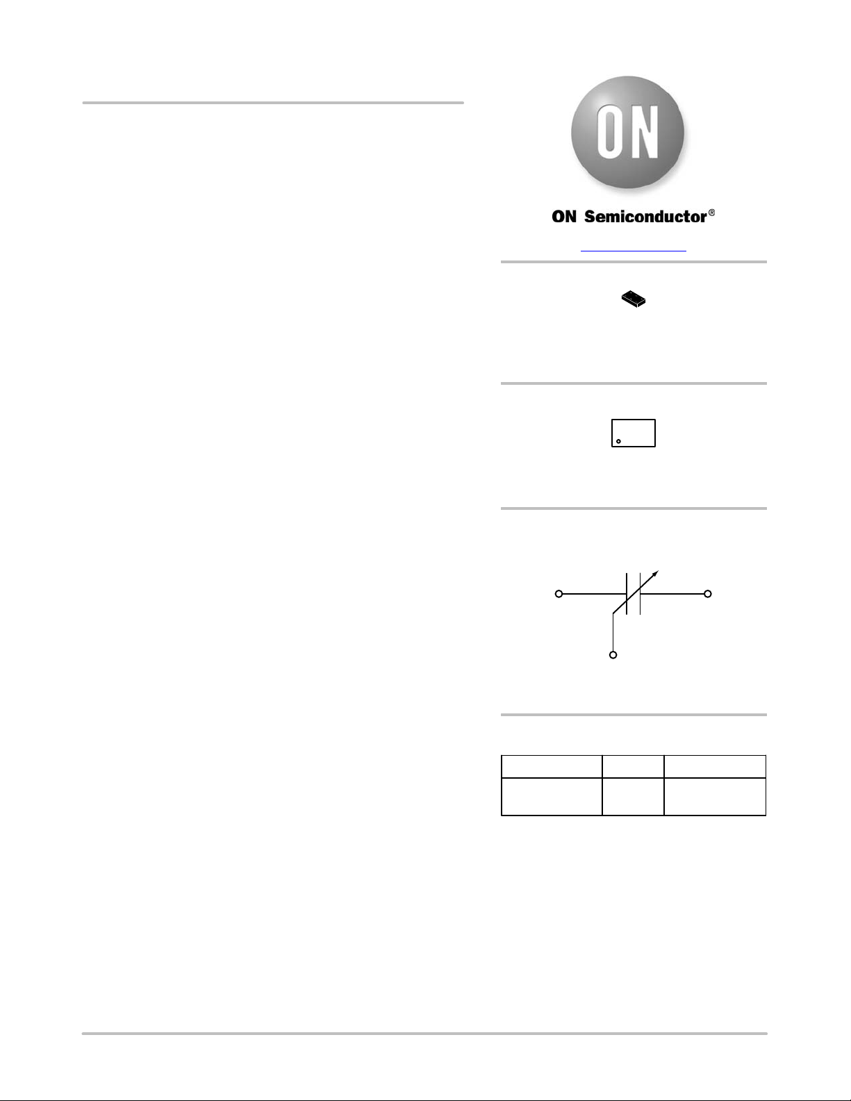
FUNCTIONAL BLOCK DIAGRAM
PTIC
RF1 RF2
Bias
PTIC Functional Block Diagram
ORDERING INFORMATION
Device Package Shipping
TCP−5012UB−DT WLCSP6
(Pb−Free)
†For information on tape and reel specifications,
including part orientation and tape sizes, please
refer to our Tape and Reel Packaging Specification
Brochure, BRD801 1/D.
4000 Units /
7” Tape & Reel
†
© Semiconductor Components Industries, LLC, 2016
November, 2016 − Rev. 0
1 Publication Order Number:
TCP−5012UB/D
Page 2
TCP−5012UB
DC Bias 1
RF2
RF2
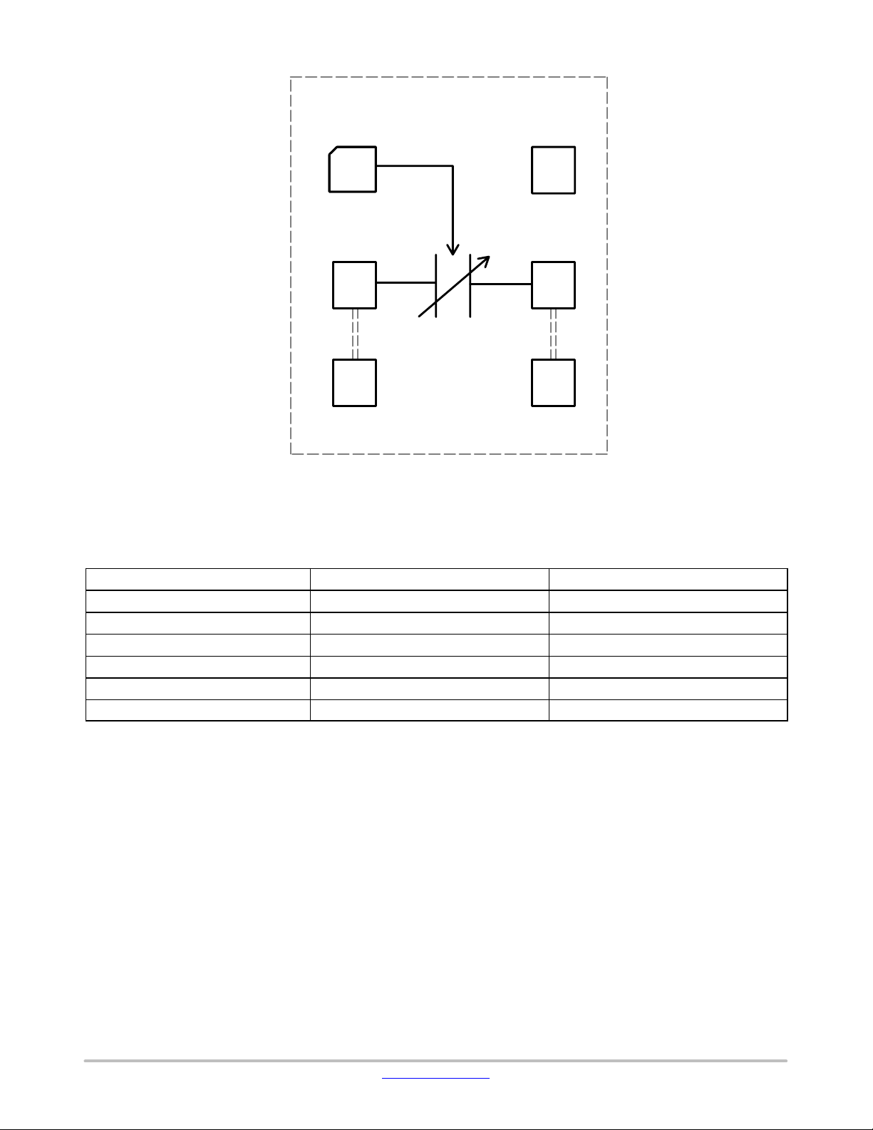
Table 1. SIGNAL DESCRIPTIONS
Ball / Pad Number Pin Name Description
A1 DC Bias 1 DC Bias Voltage
B1 RF2 RF Output
C1 RF2 RF Output
A2 NC Not Connected
B2 RF1 RF Input
C2 RF1 RF Input
A1
B1
C1
A2
B2
C2
Figure 1. PTIC Functional Block Diagram
(Top View)
NC
RF1
RF1
www.onsemi.com
2
Page 3
TCP−5012UB
TYPICAL SPECIFICATIONS
Representative Performance Data at 255C
Table 2. PERFORMANCE DATA
Parameter Min Typ Max Unit
Operating Bias Voltage 1.0 24 V
Capacitance (V
Capacitance (V
Tuning Range (1 V - 24 V) 4.80 5.25 6.00
Tuning Range (2 V - 24 V) 4.20 4.65 5.30
Leakage Current (V
Operating Frequency 700 2700 MHz
Quality Factor @ 700 MHz, 2 V (Note 5) 55
Quality Factor @ 700 MHz, 24 V (Note 5) 75
Quality Factor @ 2.4 GHz, 2 V (Note 5) 35
Quality Factor @ 2.4 GHz, 24 V (Note 5) 35
IP3 (V
IP3 (V
= 2 V) (Notes 1, 3 and 5) 70 dBm
bias
= 24 V) (Notes 1, 3 and 5) 80 dBm
bias
2nd Harmonic (V
2nd Harmonic (V
3rd Harmonic (V
3rd Harmonic (V
Average Transition Time (Cmin ³ Cmax) (Note 4
and 5)
Average Transition Time (Cmax ³ Cmin) (Note 4
and 5)
1. f1 = 850 MHz, f2 = 860 MHz, Pin 25 dBm/Tone
2. 850 MHz, Pin +34 dBm
3. IP3 and Harmonics are measured in the shunt configuration in a 50 W environment
4. RF
and RF
IN
5. Sample testing only. Average Transition Time for all start and stop voltage combinations between 2 V and 24 V is 50 ms.
= 2 V) 1.092 1.20 1.308 pF
bias
= 24 V) 0.235 0.258 0.281 pF
bias
= 24 V) 0.1
bias
= 2 V) (Notes 2, 3 and 5) -65 dBm
bias
= 24 V) (Notes 2, 3 and 5) -75 dBm
bias
= 2 V) (Notes 2, 3 and 5) -45 dBm
bias
= 24 V) (Notes 2, 3 and 5) -75 dBm
bias
66
48
are both connected to DC ground
OUT
mA
ms
ms
www.onsemi.com
3
Page 4

TCP−5012UB
Representative performance data at 255C for 1.2 pF WLCSP Package
Figure 2. Capacitance
Figure 3. Harmonic Power*
Figure 4. IP3*
Figure 5. Q*
*Data shown is representative only.
Table 3. ABSOLUTE MAXIMUM RATINGS
Parameter Rating Units
Input Power +40 dBm
Bias Voltage +30 (Note 6) V
Operating Temperature Range −30 to +85 °C
Storage Temperature Range −55 to +125 °C
ESD − Human Body Model Class 1B JEDEC HBM Standard (Note 7)
Stresses exceeding those listed in the Maximum Ratings table may damage the device. If any of these limits are exceeded, device functionality
should not be assumed, damage may occur and reliability may be affected.
6. WLCSP: Recommended Bias Voltage not to exceed 24 V.
7. Class 1B defined as passing 500 V, but may fail after exposure to 1000 V ESD pulse.
www.onsemi.com
4
Page 5

TCP−5012UB
ASSEMBLY CONSIDERATIONS AND REFLOW PROFILE
The following assembly considerations should be observed:
Cleanliness
These chips should be handled in a clean environment.
Electro-static Sensitivity
ON Semiconductor’s PTICs are ESD Class 1B sensitive.
The proper ESD handling procedures should be used.
Mounting
The WLCSP PTIC is fabricated for Flip Chip solder
mounting. Connectivity to the RF and Bias terminations on
the PTIC die is established through SAC305 solder balls
with 90 mm nominal height (65 mm to 115 mm height
variation). The PTIC die is RoHS-compliant and compatible
with lead-free soldering profile.
Molding
The PTIC die is compatible for over-molding or
under-fill.
ORIENTATION OF THE PTIC FOR OPTIMUM LOSSES
Figure 6. Reflow Profile
When configuring the PTIC in your specific circuit
design, at least one of the RF terminals must be connected
to DC ground. If minimum transition times are required, DC
ground on both RF terminals is recommended. To minimize
losses, the PTIC should be oriented such that RF2
is at the
lower RF impedance of the two RF nodes. A shunt PTIC, for
example, should have RF2
connected to RF ground.
RF ANT
RF1
(PTIC Pad)
RF2
(PTIC Pad)
Bias
Figure 7. PTIC Orientation Functional Block
Diagram
www.onsemi.com
5
Page 6

TCP−5012UB
PART NUMBER DEFINITION
Table 4. PART NUMBERS
Capacitance
Part Number
TCP−5012UB−DT 1.20 0.258 A YW** 6−bump WLCSP
*See PTIC package dimensions on following page.
**Refer to table below (Table 5) for YW trace code.
2 V 24 V
Device ID Trace Code
For information on device numbering and ordering codes, please download the Device Nomenclature technical note
(TND310/D) from www.onsemi.com
Table 5. Two Digits Year and Work Week Date coding (YW) − In Process Product / Traceability Date Code Marking
Code
YW Year and
Term Definition
Work Week
.
Two−character Alpha Code. Example: 2005, workweek 10 = GJ
Marking
Package*
YEAR WORK
WEEK
2003 1
26
27
52
2006 1
26
27
52
2009 1
26
27
52
2012 1
26
27
52
2015 1
26
27
52
CODE YEAR WORK
CA
CZ
DA
DZ
IA
IZ
JA
JZ
PA
PZ
RA
RZ
WA
WZ
XA
XZ
CA
CZ
DA
DZ
2004 1
2007 1
2010 1
2013 1
2016 1
WEEK
26
27
52
26
27
52
26
27
52
26
27
52
26
27
52
CODE YEAR WORK
EA
EZ
FA
FZ
KA
KZ
LA
LZ
SA
SZ
TA
TZ
YA
YZ
ZA
ZZ
EA
EZ
FA
FZ
2005 1
2008 1
2011 1
2014 1
2017 1
WEEK
26
27
52
26
27
52
26
27
52
26
27
52
26
27
52
CODE
GA
GZ
HA
HZ
MA
MZ
NA
NZ
UA
UZ
VA
VZ
AA
AZ
BA
BZ
GA
GZ
HA
HZ
For dates outside of the table: the first character of the code is incremented at the start of workweek 01 and workweek 27
each year . The second character begins with “A” in workweek 01 of each year and increments weekly. “A” follows “Z” to make
the code continuous.
ParaScan is a trademark of Paratek Microwave, Inc.
www.onsemi.com
6
Page 7

È
MECHANICAL CASE OUTLINE
PACKAGE DIMENSIONS
SCALE 4:1
WLCSP6, 1.097x0.622
CASE 567NZ
ISSUE A
DATE 27 SEP 2016
REFERENCE
2X
2X
NOTE 3
DETAIL A
PIN A1
0.05 C
0.05
0.06 C
0.05 C
E
C
TOP VIEW
DETAIL C
A1
SIDE VIEW
e
C
B
A
12
BOTTOM VIEW
e/2
A B
D
A
C
e
6X
b1
6X
DETAIL A
NOTE 4
TAPE
DETAIL C
SEATING
PLANE
RECOMMENDED
SOLDERING FOOTPRINT*
0.40
PACKAGE
OUTLINE
A1
NOTES:
1. DIMENSIONING AND TOLERANCING PER
ASME Y14.5M, 1994.
b
A0.05 BC
0.03
C
A3
2. CONTROLLING DIMENSION: MILLIMETERS.
3. COPLANARITY APPLIES TO SPHERICAL
CROWNS OF SOLDER BALLS.
4. BACKSIDE TAPE APPLIED TO IMPROVE
PIN 1 MARKING.
MILLIMETERS
DIMAMIN NOM
0.295
A1
0.065 0.090
A3 0.025 REF
b 0.125 0.150
b1 0.075 0.100
D 1.047 1.097
E 0.572 0.622
e 0.40 BSC
0.335
MAX
0.375
0.115
0.175
0.125
1.147
0.672
GENERIC
MARKING DIAGRAM*
XYW
X = Specific Device Code
Y = Year
W = Work Week
*This information is generic. Please refer to
device data sheet for actual part marking.
Pb−Free indicator, “G” or microdot “ G”,
may or may not be present.
0.40
PITCH
6X
DIMENSIONS: MILLIMETERS
0.20
*For additional information on our Pb−Free strategy and soldering
details, please download the ON Semiconductor Soldering and
Mounting Techniques Reference Manual, SOLDERRM/D.
DOCUMENT NUMBER:
DESCRIPTION:
ON Semiconductor and are trademarks of Semiconductor Components Industries, LLC dba ON Semiconductor or its subsidiaries in the United States and/or other countries.
ON Semiconductor reserves the right to make changes without further notice to any products herein. ON Semiconductor makes no warranty, representation or guarantee regarding
the suitability of its products for any particular purpose, nor does ON Semiconductor assume any liability arising out of the application or use of any product or circuit, and specifically
disclaims any and all liability, including without limitation special, consequential or incidental damages. ON Semiconductor does not convey any license under its patent rights nor the
rights of others.
98AON11898G
WLCSP6, 1.097X0.622
Electronic versions are uncontrolled except when accessed directly from the Document Repository.
Printed versions are uncontrolled except when stamped “CONTROLLED COPY” in red.
PAGE 1 OF 1
© Semiconductor Components Industries, LLC, 2019
www.onsemi.com
Page 8

ON Semiconductor and are trademarks of Semiconductor Components Industries, LLC dba ON Semiconductor or its subsidiaries in the United States and/or other countries.
ON Semiconductor owns the rights to a number of patents, trademarks, copyrights, trade secrets, and other intellectual property. A listing of ON Semiconductor’s product/patent
coverage may be accessed at www.onsemi.com/site/pdf/Patent−Marking.pdf
ON Semiconductor makes no warranty, representation or guarantee regarding the suitability of its products for any particular purpose, nor does ON Semiconductor assume any liability
arising out of the application or use of any product or circuit, and specifically disclaims any and all liability, including without limitation special, consequential or incidental damages.
Buyer is responsible for its products and applications using ON Semiconductor products, including compliance with all laws, regulations and safety requirements or standards,
regardless of any support or applications information provided by ON Semiconductor. “Typical” parameters which may be provided in ON Semiconductor data sheets and/or
specifications can and do vary in different applications and actual performance may vary over time. All operating parameters, including “Typicals” must be validated for each customer
application by customer’s technical experts. ON Semiconductor does not convey any license under its patent rights nor the rights of others. ON Semiconductor products are not
designed, intended, or authorized for use as a critical component in life support systems or any FDA Class 3 medical devices or medical devices with a same or similar classification
in a foreign jurisdiction or any devices intended for implantation in the human body. Should Buyer purchase or use ON Semiconductor products for any such unintended or unauthorized
application, Buyer shall indemnify and hold ON Semiconductor and its officers, employees, subsidiaries, affiliates, and distributors harmless against all claims, costs, damages, and
expenses, and reasonable attorney fees arising out of, directly or indirectly, any claim of personal injury or death associated with such unintended or unauthorized use, even if such
claim alleges that ON Semiconductor was negligent regarding the design or manufacture of the part. ON Semiconductor is an Equal Opportunity/Affirmative Action Employer. This
literature is subject to all applicable copyright laws and is not for resale in any manner.
. ON Semiconductor reserves the right to make changes without further notice to any products herein.
PUBLICATION ORDERING INFORMATION
LITERATURE FULFILLMENT:
Email Requests to: orderlit@onsemi.com
ON Semiconductor Website: www.onsemi.com
TECHNICAL SUPPORT
North American Technical Support:
Voice Mail: 1 800−282−9855 Toll Free USA/Canada
Phone: 011 421 33 790 2910
Europe, Middle East and Africa Technical Support:
Phone: 00421 33 790 2910
For additional information, please contact your local Sales Representative
◊
www.onsemi.com
1
 Loading...