

Page 1

TCC-202
f
Two-Output PTIC Control IC
Introduction
TCC−202 is a two−output high−voltage digital to analog control IC
specifically designed to control and bias ON Semiconductor’s Passive
Tunable Integrated Circuits (PTICs).
These tunable capacitor control circuits are intended for use in
mobile phones and dedicated RF tuning applications. The
implementation of ON Semiconductor’s tunable circuits in mobile
phones enables significant improvement in terms of antenna radiated
performance.
The tunable capacitors are controlled through a bias voltage ranging
from 1 V to 24 V. The TCC−202 high−voltage PTIC control IC has
been specifically designed to cover this need, providing two
independent high−voltage outputs that control up to two different
tunable PTICs in parallel. The device is fully controlled through a
MIPI interface.
Key Features
• Controls ON Semiconductor’s PTIC Tunable Capacitors
• Compliant with Timing Needs of Cellular and Other Wireless System
Requirements
• Integrated Boost Converter with 2 Programmable DAC Outputs
(up to 24 V)
• Low Power Consumption
• MIPI−RFFE Interface
• Compliant with MIPI 26 MHz Read−back
• Available in WLCSP (RDL ball arrays)
• This is a Pb−Free Device
www.onsemi.com
WLCSP12
CASE 567KZ
MARKING DIAGRAM
XXXX
ALYW
G
A = Assembly Location
L = Wafer Lot
Y = Year
W = Work Week
G = Pb−Free Package
ORDERING INFORMATION
See detailed ordering and shipping information on page 21 o
this data sheet.
Typical Applications
• Multi−band, Multi−standard, Advanced and Simple Mobile Phones
• Tunable Antenna Matching Networks
• Compatible with Closed−loop and Open−loop Antenna Tuner
Applications
© Semiconductor Components Industries, LLC, 2016
September, 2016 − Rev. 3
1 Publication Order Number:
TCC−202/D
Page 2
TCC−202
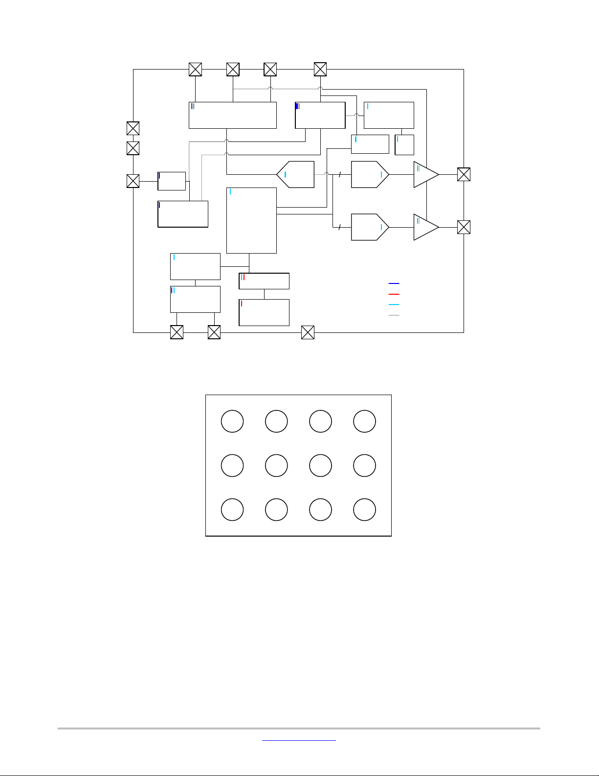
VDDA
GND
VIO
L_BOOST VHV
VIO
POR
Start
Reference
Interface
Level
Shifter
Booster
Registers
GND_BOOST
vio_on
ibias_start / vref_start
Level
Shifter
OTP
VREG
Regulator
4 bit
DAC
por_vreg
Bandgap
VREG
POR
7 bit
7
DAC
7 bit
7
DAC
RC
OSC
OUTA
OUTB
VIO
VDDA
VREG
VHV
CLK DATA
Figure 1. Control IC Functional Block Diagram
ATEST
A4
B4
C4
A3
B3
C3
A2
B2
C2
Figure 2. Die Bump Side View
A1
B1
C1
www.onsemi.com
2
Page 3
TCC−202
RDL Pin Out
Table 1. PAD DESCRIPTIONS
Bump RDL Name Type Description
A1 OUTB AOH High Voltage Output B
A2 ATEST AO Analog Test Out (Note 1)
A3 VHV AOH/AIH Boost High Voltage
A4 L_BOOST AOH Boost Inductor
B1 OUTA AOH High Voltage Output A
B2 GNDA P Analog Ground
B3 GND_BOOST P Ground for Booster
B4 VIO Digital IO Supply
C1 VREG AO Regulator Output
C2 AVDD Analog Supply
C3 DATA DIO MIPI RFFE Data
C4 CLK DI MIPI RFFE Clock
1. To be grounded when not in use.
Legend: Pad Types
AIH = High Voltage Analog Input
AO = Analog Input
AOH = High Voltage Analog Input
DI = Digital Input
DIO = Digital Input/Output (IO)
P = Power
ELECTRICAL PERFORMANCE SPECIFICATIONS
Table 2. ABSOLUTE MAXIMUM RATINGS
Symbol Parameter Rating Unit
AVDD Analog Supply Voltage −0.3 to +6.0 V
VIO IO Reference Supply Voltage −0.3 to +2.5 V
V
I/O
V
HVH
V
ESD (HBM)
V
ESD (MM)
T
STG
T
AMB_OP_MAX
Stresses exceeding those listed in the Maximum Ratings table may damage the device. If any of these limits are exceeded, device functionality
should not be assumed, damage may occur and reliability may be affected.
Input Voltage Logic Lines (DATA, CLK, CS) −0.3 to VIO + 0.3 V
VHV Maximum Voltage −0.3 to 30 V
Human Body Model, JESD22−A114, All I/O 2,000 V
Machine Model, JESD22−A115 200 V
Storage Temperature −55 to +150 °C
Max Operating Ambient Temperature without Damage +110 °C
www.onsemi.com
3
Page 4
TCC−202
Table 3. RECOMENDED OPERATING CONDITIONS
Rating
Symbol Parameter
T
AMB_OP
T
J_OP
Operating Ambient Temperature −30 − +85 °C
Operating Junction Temperature −30 − +125 °C
AVDD Analog Supply Voltage 2.3 − 5.5 V
VIO IO Reference Supply Voltage 1.62 − 1.98 V
Min Typ Max
Unit
Table 4. DC CHARACTERISTICS (T
= equivalent series load of 5.6 kW and 2.7 nF; CHV = 47 nF; L
R
LOAD
Symbol
Parameter Min Typ Max Unit Comment
= −30 to +85°C; V
A
SHUTDOWN MODE
I
AVDD
I
L_BOOST
I
BATT
I
VIO
I
CLK
I
DATA
AVDD Supply Current − − 1.5 mA
L_BOOST Leakage − − 1.5
Battery Current − − 2.5
VIO Supply Current −1 − 1
CLK Leakage −1 − 1
DATA Leakage −1 − 1
ACTIVE MODE
I
BATT_SS0
I
BAT_SS2
I
BATT_SS16
I
L_BOOST_SS0
I
L_BOOST_SS2
I
L_BOOST_SS16
I
VIO_INACT
I
VIO_ACTIVE
V
VREG
Average battery current, 2 outputs @
0 V steady state
Average battery current, 2 outputs @
2 V steady state
Average battery current, 2 outputs @
16 V steady state
Average inductor current, 2 outputs @
0 V steady state
Average inductor current, 2 outputs @
2 V steady state
Average inductor current, 2 outputs @
16 V steady state
VIO average inactive current − − 3 VIO is high, no bus activity
VIO average active current − − 250 VIO = 1.8 V, master sending
LOW POWER MODE
I
AVDD
I
L_BOOST
I
BATT
I
VIO
V
VREG
AVDD Supply Current − − 8 mA
L_BOOST Leakage − − 6
Battery Current − − 14 I
VIO Supply Current − − 3 No bus activity
= 15 V for each output; 2.3 V < AVDD < 5.5 V; 1.62 V < VIO < 1.98 V;
OUTX
= 15 mH; unless otherwise specified)
BOOST
VIO Supply is Low
− 380 750
mA
At VHV = 20 V
AVDD = 3.3 V
− 400 780 mA At VHV = 20 V
AVDD = 3.3 V
− 510 870 At VHV = 20 V
AVDD = 3.3 V
− 260 490 At VHV = 20 V
AVDD = 3.3 V
− 280 510 At VHV = 20 V
AVDD = 3.3 V
− 400 600 At VHV = 20 V
AVDD = 3.3 V
data at 26 MHz
1.7 − 1.9 V No external load allowed
+ I
AVDD
L_BOOST
1.6 − 1.9 V No external load allowed
www.onsemi.com
4
Page 5
TCC−202
Table 5. BOOST CONVERTER CHARACTERISTICS
(AVDD from 2.3 V to 5.5 V; VIO from 1.62 V to 1.98 V; TA = –30 to +85°C; CHV = 47 nF; L
Symbol
VHV_min Minimum programmable output volt-
Parameter Conditions Min Typ Max Unit
Active mode − 13 −
age (average), DAC Boost = 0h
VHV_max Maximum programmable output volt-
Active mode − 28 −
age (average), DAC Boost = Fh
Resolution Boost voltage resolution 4−bit DAC − 1 −
I
L_BOOST_LIMIT
Inductor current limit − 200 − mA
Table 6. ANALOG OUTPUTS (OUT A, OUT B)
(AVDD from 2.3 V to 5.5 V; VIO from 1.62 V to 1.98 V; VHV = 26 V; TA = –30 to +85°C; Rload = ∞ unless otherwise specified)
Parameter
SHUTDOWN MODE
Z
OUT
OUT A, OUT B output impedance 7 − −
ACTIVE MODE
V
OH
V
OL
Maximum output voltage − 23.8 − V DAC A, B = 7Fh,
Minimum output voltage − − 1 V DAC A, B = 01h, DAC
Slew Rate − 3 10
R
PD
OUT A, OUT B set in pull−down
mode
Resolution Voltage resolution (1−bit) − 188 − mV (1 LSB = 1−bit)
V
OFFSET
Zero scale, least squared best fit −1 − +1 LSB
Error −3.0 − +3.0 %V
DNL Differential non−linearity least
squared best fit
INL Integral non−linearity least squared
best fit
I
V
RIPPLE
SC
Over current protection − 5 65 mA Any DAC output shorted to ground
Output ripple with all outputs at
steady state
Description Min Typ Max Unit Comment
− − 1000
−0.9 − +0.9 LSB Over 2 V – 24 V VO range
−1 − +1 LSB Over 2 V – 24 V VO range
− − 40 mV RMS Over 2 V – 24 V for VHV = 23.5 V
= 15 mH; unless otherwise specified)
BOOST
MW
DAC disabled
DAC Boost = Fh, I
Boost = 0h to Fh, I
ms
W
2 V to 24 V step, measured at
V
= 15.2 V,
OUT
R
= equivalent series load of
LOAD
2.7 kW and 5.6 nF, Turbo enabled
DAC A, B = 00h, DAC Boost = 0h to
Fh, selected output(s) is disabled
OUT
Over 2 V – 24 V VO range
< 10 mA
OH
< 10 mA
OH
V
www.onsemi.com
5
Page 6
TCC−202
THEORY OF OPERATION
Overview
The control IC outputs are directly controlled by
programming the two DACs (DAC A and DAC B) through
the digital interface.
The DAC stages are driven from a reference voltage,
generating an analog output voltage driving a high−voltage
amplifier supplied from the boost converter (see Figure 1 −
Control IC Functional Block Diagram).
The control IC output voltages are scaled from 0 V to
24 V, with 128 steps of 188 mV (2x (24 / 255 V) =
0.188235 V). The nominal control IC output can be
approximated to 188 mV x DAC value.
For performance optimization the boost output voltage
(VHV) can be programmed to levels between 13 V and 28 V
via the DAC_boost register (4 bits with 1 V steps). The
startup default level for the boosted voltage is VHV = 24 V.
For proper operation and to avoid saturation of the output
devices and noise issues it is recommended to operate the
boosted VHV voltage at least 2 V above the highest
programmed V
Operating Modes
voltage of any of the two outputs.
OUT
The following operating modes are available:
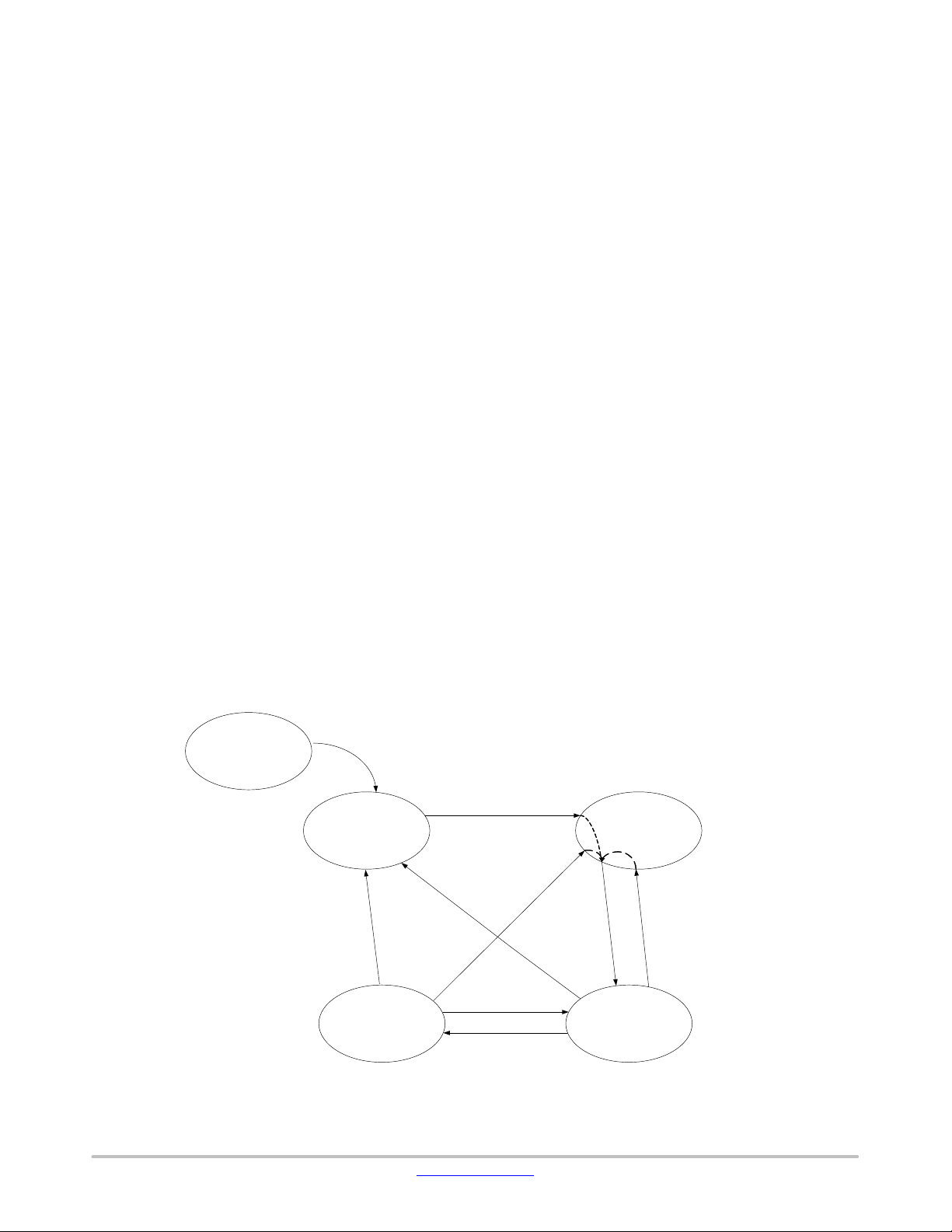
1. Shutdown Mode: All circuit blocks are off, the
DAC outputs are disabled and placed in high Z
state and current consumption is limited to
minimal leakage current. The shutdown mode is
entered upon initial application of AVDD or upon
VIO being placed in the low state. The contents of
the registers are not maintained in shutdown mode.
2. Startup Mode: Startup is only a transitory mode.
Startup mode is entered upon a VIO high state. In
startup mode all registers are reset to their default
states, the digital interface is functional, the boost
converter is activated, outputs OUT A and OUT B
are disabled and the DAC outputs are placed in a
high Z state. Control software can request a full
hardware and register reset of the TCC−202 by
sending an appropriate PWR_MODE command to
direct the chip from either the active mode or the
low power mode to the startup mode. From the
startup mode the device automatically proceeds to
the active mode.
3. Active Mode: All blocks of the TCC−202 are
activated and the DAC outputs are fully controlled
through the digital interface, DACs remain off
until enabled. The DAC settings can be
dynamically modified and the HV outputs will be
adjusted according to the specified timing
diagrams. Each DAC can be individually
controlled and/or switched off according to
application requirements. Active mode is
automatically entered from the startup mode.
Active mode can also be entered from the low
power mode under control software command.
4. Low Power Mode: In low power mode the serial
interface stays enabled, the DAC outputs are
disabled and are placed in a high Z state and the
boost voltage circuit is disabled. Control software
can request to enter the low power mode from the
active mode by sending an appropriate
PWR_MODE command. The contents of all
registers are maintained in the low power mode.
VDDA = 0
Shutdown
VIO = LOW
(User Defined)
Battery insertion
VIO = HIGH
PWR_MODE =
VIO = LOW
PWR_MODE = 0b00
Low Power
PWR_MODE = 0b10
Figure 3. Modes of Operation
www.onsemi.com
6
Startup
(Registers reset)
0b01
PWR_MODE =
0b01
automatic
Active
(User Defined)
Page 7
TCC−202
AVDD Power−On Reset (POR)
Upon application of AVDD the TCC−202 will be in
shutdown mode. All circuit blocks are off and the chip draws
only minimal leakage current.
VIO Power−On Reset and Startup Conditions
A high level on VIO places the chip in startup mode which
provides a POR to the TCC−202. POR resets all registers to
their default settings as described in T able 8. VIO POR also
resets the serial interface circuitry . POR is not a brown−out
detector and VIO needs to be brought back to a low level to
enable the POR to trigger again.
Table 7. VIO POWER−ON RESET AND STARTUP
Default State for
Register
DAC Boost [1011] VHV = 24 V
Power Mode [01]>[00] Transitions from shutdown to startup and then automatically to active mode
DAC Enable [000000] V
DAC A Output in High−Z Mode
DAC B Output in High−Z Mode
VIO POR
A, B Disabled
OUT
Comment
VIO Shutdown
A low level at any time on VIO places the chip in shutdown mode in which all circuit blocks are off. The contents of the
registers are not maintained in shutdown mode.
Table 8. VIO THRESHOLDS (AVDD from 2.3 V to 5.5 V; T
Parameter
VIORST VIO Low Threshold − − 0.2 V When VIO is lowered below this threshold level the
Description Min Typ Max Unit Comments
= –30 to +85°C unless otherwise specified)
A
chip is reset and placed into the shutdown state
Power Supply Sequencing
The AVDD input i s typically d irectly s upplied f rom t he b attery a nd t hus i s t he f irst o n. A fter AVDD is applied a nd b efore V IO
is applied to the chip, all circuits are in the shutdown state and draw minimum leakage currents. Upon application of VIO, the
chip automatically starts up using default settings and is placed in the active state waiting for a command via the serial interface.
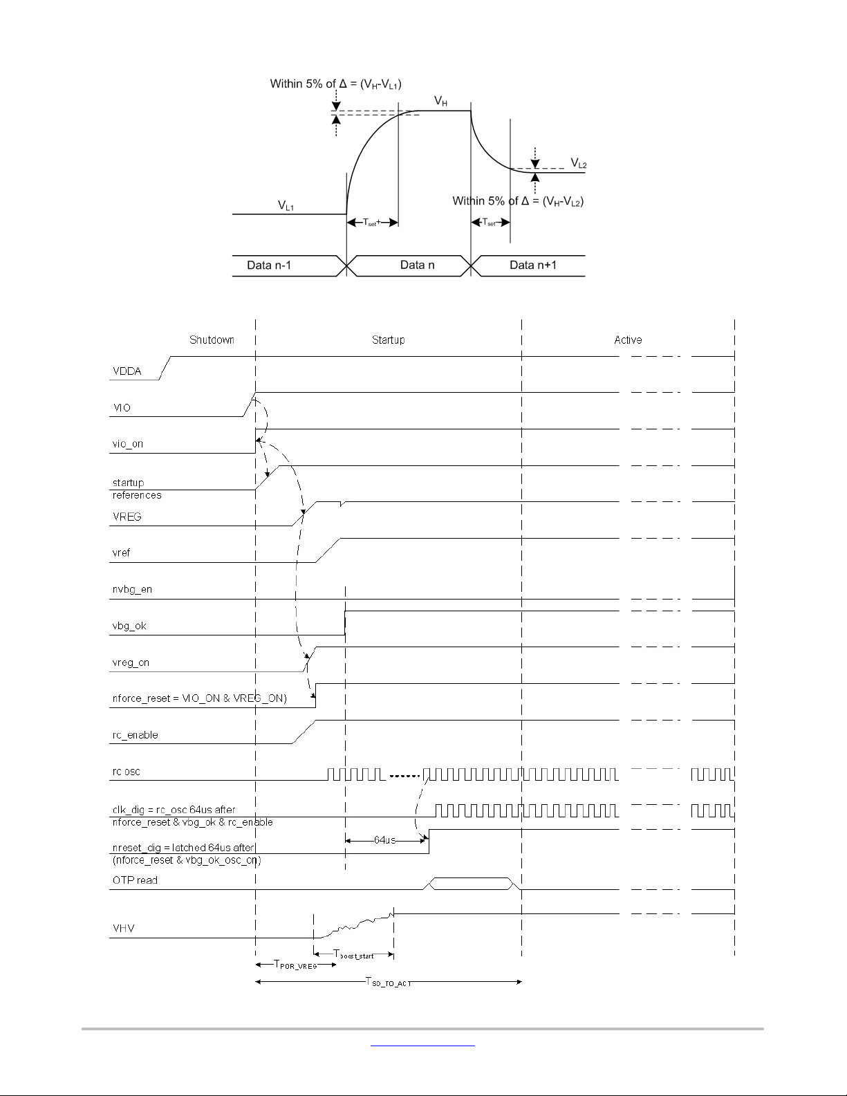
Table 9. TIMING (AVDD from 2.3 V to 5.5 V; VIO from 1.62 V to 1.98 V; T
= 15 mH; VHV = 24 V; Turbo−Charge mode off unless otherwise specified; VDDA = 1.7 V)
Parameter
T
POR_VREG
T
BOOST_START
T
SD_TO_ACT
T
SET+
T
SET−
T
SET+
T
SET−
Internal bias settling time from shutdown to active mode − 50 120
Time to charge CHV @ 80% of set VHV
(set to 24 V, V
Startup time from shutdown to active mode − 180 300
Output A, B positive settling time to within 5% of the
delta voltage, equivalent series load of 5.6 kW and 2.7
nF, V
Output A, B negative settling time to within 5% of the
delta voltage, equivalent series load of 5.6 kW and 2.7
nF, V
Output A, B positive settling time with Turbo − 35 −
Output A, B negative settling time with Turbo − 35 −
from 2 V to 20 V; 0Bh (11d) to 55h (85d)
OUT
from 20 V to 2 V; 55h (85d) to 0Bh (11d)
OUT
Description Min Typ Max Unit Comments
= 2.7 V)
DDA
= –30 to +85°C; OUT A and OUT B; CHV = 47 nF; L
A
For info only
For info only
Voltage settling time
connected on V
A, B
Voltage settling time
connected on V
A, B
Voltage settling time
connected on V
A, B
Voltage settling time
connected on V
A, B
− 130 −
− 50 60
− 50 60
ms
ms
ms
ms
ms
ms
ms
BOOST
OUT
OUT
OUT
OUT
www.onsemi.com
7
Page 8
TCC−202
Figure 5. Startup Timing Diagram
Figure 4. Output Settling Diagram
www.onsemi.com
8
Page 9

TCC−202
Boost Control
The TCC−202 integrates an asynchronous current control
boost converter. It operates in a discontinuous mode and
features spread−spectrum circuitry for Electro−Magnetic
Interference (EMI) reduction. The average boost clock is
2 MHz and the clock is spread between 0.8 MHz and 4 MHz.
Boost Output Voltage (VHV) Control Principle
The asynchronous control starts the boost converter as
soon as the VHV voltage drops below the reference set by
the 4−bit DAC and stops the boost converter when the VHV
voltage rises above the reference again.
Recharge
S
e
t
V
H
V
Figure 6. VHV Voltage Waveform
CHV
Delay
Due to the slow response time of the control loop, the
VHV voltage may drop below the set voltage before the
control loop compensates for it. In the same manner, VHV
can rise higher than the set value. This effect may reduce the
maximum output voltage available. Please refer to Figure 7
below.
The asynchronous control reduces switching losses and
improves the output (VHV) regulation of the DC/DC
converter under light load, particularly in the situation
where the TCC−202 only maintains the output voltages to
fixed values.
CHV
Boost
Running
Discharge
Delay
VHV
Delay
Time
High Impedance (High Z) Feature
In shutdown mode the OUT pins are set to a high
impedance mode (high Z). Following is the principle of
operation for the control IC:
1. The DAC output voltage V
OUT
DAC code
+
255
24 V 2
V
is defined by:
OUT
(eq. 1)
2. The voltage VHV defines the maximum supply
voltage of the DAC supply output regulator and is
set by a 4−bit control.
3. The maximum DAC DC output voltage V
OUT
is
limited to (VHV – 2 V).
4. The minimum output DAC voltage V
OUT
is 1.0 V
max.
Figure 8. DAC Output Range Example B
Digital Interface
The control IC is fully controlled through a MIPI
RFFE−compliant digital interface The digital interface is
described in the following sections of this document, for
detailed programming instructions please refer to the
programming guide, available by contacting
ON Semiconductor.
Figure 7. DAC Output Range Example A
www.onsemi.com
9
Page 10

TCC−202
Turbo−Charge Mode
The TCC−202 control IC has a Turbo−Charge mode that
significantly shortens the system settling time when
changing programming voltages. In Turbo−Charge mode
the DAC output target voltage is temporarily set to either a
delta voltage above or a delta voltage below the actual
desired target for the TCDLY time. It is recommended that
V
be set to 24 V when using Turbo−Charge mode.
HV
Glide Mode
Unlike turbo mode, which is intended to reduce the
charging time, the glide mode extends the transition time of
each DAC output. Each DAC has an individual control for
turbo mode, glide mode or regular voltage switching. The
glide mode can be enabled for a particular DAC through the
INDEX register, by setting DAC State to ‘1’ when glide
mode is enabled, turbo mode is off for a particular DAC, but
one DAC can be gliding while the other is turbo.
CLK
TD
SETUP
TD
HOLD
During glide mode the output voltage of a DAC is either
increased or dec reased to its set end point, in max 255 steps,
where each DAC time step can be programmed between
2 ms to 64 ms. For programming the glide mode refer to the
application note (coming soon). A programming input is not
required to maintain a glide transition, all step controls are
maintained by the part. Only the inputs to define the glide
need to be programmed.
RF Front−End Control Interface (MIPI RFFE Interface)
The TCC−202 is a read/write slave device which is fully
compliant to the MIPI Alliance Specification for RF
Front−End Control Interface (RFFE) Version 1.10.00 26
July 2011. This device is rated at full−speed operation for
1.62 V<VIO<1.98 V.
TD
SETUP
TD
HOLD
DATA
Figure 9. MIPI−RFFE Signal Timing during Master Writes to PTIC Control IC
CLK
DATA
T
READ_ACCESS
T
SDATAOTR
T
READ_ACCESS
T
SDATAOTR
Figure 10. MIPI−RFFE Signal Timing during Master
Reads from PTIC Control IC
CLK
DATA
T
SDATAZ
Bus Park Cycle
Figure 11. Bus Park Cycle Timing
when MIPI−RFFE Master Reads
from PTIC Control IC
www.onsemi.com
10
Page 11

TCC−202
Table 10. MIPI RFFE INTERFACE SPECIFICATION
(TA = −30 to +85°C; 2.3 V < VDDA < 5.5 V; 1.62 < VIO < 1.98 V; unless otherwise specified)
Parameter
F
SCLK
T
SCLK
T
SCLKIH
T
SCLKIL
TD
SETUP
TD
HOLD
T
READ_ACCESS
T
READ_ACCESS
The control IC contains thirteen 8−bit registers. Register content is described in Table 11. Some additional registers
implemented as provision, are not described in this document.
Description Min Typ Max Unit Comments
Clock Full−Speed
Frequency
Clock Full−Speed Period 0.038 − 32
0.032 − 26 MHz Full−Speed Operation:
1.62 V< VIO < 1.98 V
ms
Full−Speed Operation:
1.62 V< VIO < 1.98 V
CLK Input High Time 11.25 − − ns Full−Speed
CLK Input Low Time 11.25 − − ns Full−Speed
Write DATA Setup Time −1 − 1 ns Full−Speed
Write DATA Hold Time −5 − 5 ns Full−Speed
Read DATA valid from
CLK rising edge
− − 7.11 ns Full Speed at VIO = 1.80 V,
= 25°C and max 15 pF load on
DATA pin
Read DATA valid from
CLK rising edge
− − 9.11 ns Full Speed at VIO = 1.80 V,
= 25°C and max 50 pF load on
DATA pin
Table 11. MIPI RFFE ADDRESS MAP
Register
Address
Description Purpose
0x00 DAC Configuration (Enable Mask) High voltage output enable mask Write 7
0x01 Turbo Register DAC A, B Turbo−charge configuration DAC A, B (Note 2) Write 8
0x02 DAC A Register OUT A value [6:0] Write 8
0x03 DAC B Register OUT B value [6:0] Write 8
0x09 Wake Up Wake−Up Controls Write 8
0x10 Boost Voltage (VHV) Settings for the boost high voltage Write 8
0x12 Turbo−Charge Delay DAC A, B Turbo−charge delay steps
DAC A, B
0x13 Turbo−Charge Delay DAC A, B Turbo−charge delay, multiplication
DAC A, B
0x1A MIPI−RFFE STATUS Detect MIPI protocol errors Read/Write 8
0x1B RFFE Group SID MIPI RFFE group slave Write 8
0x1C Power Mode and Trigger Register Power mode & trigger control Write 8
0x1D Product ID Register Product number (Notes 3 and 5) Write 8
0x1E Manufacturer ID Register MN (10 bits long)
Manufacturer ID[7:0] (Note 4)
0x1F Unique Slave Identifier Register (USID) Spare [7:6]
[5,4] = Manufacturer ID [9:8]
0x2C Glide Timer Settings [6:5] Turbo and Glide control / [4:0] Glide Timer
setting / Need extended write for this register
2. The details for configuration of Turbo mode should be ascertained from the Programming Guide, available from ON Semiconductor.
3. The two least significant bits from Product ID register are programmed in OTP during manufacture. The other six bits of Product ID are
hardcoded in ASIC.
4. Manufacture ID is hardcoded in ASIC, and mapped in a READ−only register, not programmed in OTP.
5. TCC−202 supports WRITE access to Product ID, only in respect to comply with MIPI RFFE specification 6.8.3, Programmable USID”, of
MIPI Alliance Specification for RF Front−End Control Interface (RFFE) Version 1.00.00 26 July 2011.
Access
Type
Size (bits)
Write 8
Write 8
Write 8
Write 8
Write 8
www.onsemi.com
11
Page 12

TCC−202
Table 12. REGISTER DETAILS The following are the details of the available RFFE registers:
Register RFFE:
Reset Source: nreset_dig or SWR = ‘1’ or PWR_MODE = ‘01’ (transition through STARTUP mode)
6 5 4 3 2 1 0
Bits SS Enable Reserved Reserved DAC A (Note 6) DAC B (Note 6) Reserved Reserved
Reset W−1 U−0 U−0 W−0 W−0 U−0 U−0
6. When any o f the bits [3:2] are written with ‘0’, the corresponding DAC is disabled, but the Turbo− Charge process which is a lready started, will
not be stopped.
7. If all bits [3:2] are ‘0’, then incoming DAC messages will be ignored, until at least one of [3:1] is set ‘1’.
Bit [6]: Spread Spectrum enable
0: SS disabled
1: SS enabled
Bit [3]: Control DAC A
0: off (default)
1: enabled
Bit [2]: Control DAC B
0: off (default)
1: enabled
RFFE_REG_0x00 Address RFFE A[4:0]: 0x00
Register RFFE:
Reset Source: nreset_dig or SWR = ‘1’ or PWR_MODE = ‘01’ (transition through STARTUP mode)
7 6 5 4 3 2 1 0
Bits Reserved
Reset W−0 W−0 W−0 W−0 W−0 W−0 W−0 W−0
Register RFFE: RFFE_REG_0x02 Address RFFE A[4:0]: 0x02
Reset Source: nreset_dig or SWR = ‘1’ or PWR_MODE = ‘01’ (transition through STARTUP mode)
7 6 5 4 3 2 1 0
Bits Reserved DAC A value [6:0]
Reset U−0 W−0 W−0 W−0 W−0 W−0 W−0 W−0
Register RFFE: RFFE_REG_0x03 Address RFFE A[4:0]: 0x03
Reset Source: nreset_dig or SWR = ‘1’ or PWR_MODE = ‘01’ (transition through STARTUP mode)
7 6 5 4 3 2 1 0
Bits Not Used DAC B value [6:0]
Reset W−0 W−0 W−0 W−0 W−0 W−0 W−0 W−0
TC_STP_DACx [1:0] Turbo Steps for TCDLY [us]
00 3
01 (default) 5
10 7
11 9
RFFE_REG_0x01 Address RFFE A[4:0]: 0x01
Register RFFE: RFFE_REG_0x12 Address RFFE A[4:0]: 0x12
Reset Source: nreset_dig or SWR = ‘1’ or PWR_MODE = ‘01’ (transition through STARTUP mode)
7 6 5 4 3 2 1 0
Bits Reserved Reserved TC_STP_DAC_B TC_STP_DAC_A
Reset U−0 U−0 U−0 U−0 W−0 W−1 W−0 W−1
www.onsemi.com
12
Page 13

TCC−202
Register RFFE:
Reset Source: nreset_dig or SWR = ‘1’ or PWR_MODE = ‘01’ (transition through STARTUP mode)
7 6 5 4 3 2 1 0
Bits Reserved Reserved TCM_B TCM_A
Reset U−0 U−0 U−0 U−0 W−0 W−0 W−0 W−0
TCM [1:0] Turbo Multiplication Factor
00 (default) 4
01 3
10 2
11 1
Step [us] DAC state 0 1 2 3 4 5 6 7 8 9 10 11
9 TCDLY Turbo OFF 18 27 36 45 54 63 72 81 90 99
7 TCDLY Turbo OFF 14 21 28 35 42 49 56 63 70 77
5 (default) TCDLY Turbo OFF 10 15 20 25 30 35 40 45 50 55
3 TCDLY Turbo OFF 6 9 12 15 18 21 24 27 30 33
The value of Turbo time is deducted based on the hardware comparison of new DAC value in respect to old D AC value, as follows:
If DAC new > DAC old, then T
If DAC new < DAC old, and DAC new_divby2 < 21, then T
DAC new_divby2 > 21, then T
If DAC new < DAC old, and DAC new_divby2 = 21, then T
RFFE_REG_0x13 Address RFFE A[4:0]: 0x13
UP = TCDLY
DOWN = TCDLY + TCM * (21 – DAC_new_divby2) If DAC new < DAC old, and
DOWN = TCDLY
DOWN = TCDLY
Register RFFE:
Reset Source: nreset_dig or SWR = ‘1’ or PWR_MODE = ‘01’ (transition through STARTUP mode)
7 6 5 4 3 2 1 0
Bits
Reset U−0 U−0 U−0 U−0 W−0 W−0 W−0 W−0
Reserved DAC_WAKEUP_CTRL
RFFE_REG_0x9 Address RFFE A[4:0]: 0x09
Turbo Latency Select
Reserved Reserved
Bit [3]: DAC Wake−up Control applicable to Wake−up from LP
0 : (default) Don’t apply Turbo when Wake−up from LP STD or LP FTA
1: Always apply Turbo UP when Wake−up from LP STD or LP FTA. Turbo UP is calculated based on DAC value prior to
enter LP STD or LP FTA mode.
NOTE 1: Turbo is NOT applied after Wake−up to the DACs which are programmed with 0x00 in the DAC value register
NOTE 2: Turbo is NOT applied after W ake−up from FTA mode if a trigger (Turbo, Normal, Glide) was generated while TC2x2
was in LP FTA mode
NOTE 3: When Bit[3] = ‘1’, then Turbo is applied after Wake−up regardless if:
• DAC values are updated or not
• last DAC value update is equal with old DAC value
NOTE 4: When RFFE_REG_0x31 / Wake−up DAC Ctrl is ‘0’ (default) Turbo after Wake−Up is applied after first
vhv_too_lowfalling edge is detected. When RFFE_REG_0x31 / Wake−up DAC Ctrl is ‘1’ Turbo after Wake−up is applied
after rc_clk starts.
Bit [2]: Turbo UP latency Select when Wake−up from LP.
This field has no effect when DAC_WAKEUP_CTRL[1:0] = ‘00’
0: (default) Turbo UP latency is 50 ms
1: Turbo UP latency is 100 ms
www.onsemi.com
13
Page 14

TCC−202
Register RFFE:
Reset Source: nreset_dig or SWR = ‘1’ or PWR_MODE = ‘01’ (transition through STARTUP mode)
7 6 5 4 3 2 1 0
Bits Reserved Fixed Boost voltage value
Reset U−0 U−0 U−0 U−1
RFFE_REG_0x10 Address RFFE A[4:0]: 0x10
W-1
W−0
W-1 W-1
Bit [3:0]: Boost voltage value
Register RFFE: RFFE_STATUS_0x1A Address RFFE A[4:0]: 0x1A
Reset Source: nreset_dig or SWR = ‘1’ or PWR_MODE = ‘01’ (transition through STARTUP mode)
7 6 5 4 3 2 1 0
Bits SWR CFPE CLE AFPE DFPE RURE WURE BGE
Reset W−0 R−0 R−0 R−0 R−0 R−0 R−0 R−0
RFFE_STATUS register can be read any time after power−up without the need to enable the Read Operation as described
below.
SWR Soft−Reset MIPI−RFFE registers
Write ‘1’ to this bit to reset all the MIPI−RFFE registers, except RFFE_REG_0x1C, RFFE_USID, and RFFE_GROUP_SID
This bit will always Read−back ‘0’.
The soft reset occurs in the last clock cycle of the MIPI−RFFE frame which Writes ‘1’ to this bit.
Right immediately after this frame, all the MIPI−RFFE registers have the reset value and are ready to be reprogrammed as
desired.
The OTP duplicated registers are reset to the values written in OTP.
SWR can be written only by USID messages. GSID and Broadcast frames will be ignored when writing to this register field.
RFFE_STATUS Bits [6:0] are set ‘1’ by hardware to flag when a certain condition is detected, as described below.
RFFE_STATUS Bits [6:0] cannot be written, but it is cleared to ‘0’ under following conditions:
• Hardware Self−reset is applied after RFFE_STATUS is READ
• When SWR is written ‘1’ with USID frames
• When power mode transitions through STARTUP mode ‘01’
• After Power−up Reset
CFPE
1: Command frame with parity error received.
On the occurrence of this error, the slave will ignore the entire Command Sequence
CLE
1: Incompatible command length, due to unexpected SSC received before command length to be completed.
On the occurrence of this error, the slave will accept Write data up to the last correct and complete frame. When MIPI−RFFE
multi−byte Read command is detected, the slave will always replay with an extended Read command of length of one byte.
AFPE
1: Address frame with parity error received.
On the occurrence of this error, the slave will ignore the entire Command Sequence
DFPE
1: Data frame with parity error received.
On the occurrence of this error, the slave will ignore only the erroneous data byte (s)
RURE
1: Read of non−existent register was detected.
On the occurrence of this error, the slave will not respond to the Read command frame.
When the Read Operation is not enabled ,any read from an address other than 0x1A, will set RURE and the slave will not
respond to the Read command frame.
When the Read Operation is enabled , any read from an unoccupied RFFE register address will set RURE.
WURE
1: Write to non−existent register was detected.
On the occurrence of this error, the slave discards data being written, and on the next received frame, proceeds as normal
BGE
1: Read using the Broadcast ID was detected
On the occurrence of this error, the slave will ignore the entire Command Sequence
www.onsemi.com
14
Page 15

TCC−202
Register RFFE:
Reset Source: nreset_dig or PWR_MODE = ‘01’ (transition through STARTUP mode)
7 6 5 4 3 2 1 0
Bits Reserved Reserved Reserved Reserved GSID[3] GSID[2] GSID[1]
Reset 0 0 0 0 W−0 W−0 W−0 W−0
RFFE_GROUP_SID_0x1B Address RFFE A[4:0]: 0x1B
GSID[0]
GSID = Group Slave Identifier Register
NOTE: The GSID[3:0] field can be written directly by messages using USID.
NOTE: GSID value is NOT retained during SHUTDOWN power mode.
NOTE: GSID value is not affected by SWR bit from RFFE_STATUS register
NOTE: Frames using USID = GSID, can write only to RFFE_REG_0x1C[7:6] and [2:0].
NOTE: RFFE READ frames containing GSID will be ignored
Register RFFE:
Reset Source: nreset_dig or PWR_MODE = ‘01’ (transition through STARTUP mode)
7 6 5 4 3 2 1
Bits
Reset W−0 W−0 W−0 W−0 W−0 W−0 W−0 W−0
8. Trigger Mask bits [5:3] can be changed, either set or cleared, only with an individual message using USID
9. During broadcast MIPI−RFFE accesses using GSID = ‘0000’, Trigger bits [2:0] are masked by the pre−existent setting of Trigger Mask Bits
[5:3]
10.During Individual MIPI−RFFE accesses using USID, Trigger bits [2:0] are masked by the incoming Trigger Mask bits [5:3] within the same
write message to RFFE_REG_0x1C register. During Individual MIPI−RFFE accesses using USID, pre−existent setting of Trigger Mask Bits
[5:3] is ignored.
11.When RFFE_REG_0x1C/ Trigger_Mask_2 = ‘1’ and Trigger_Mask_1 = ‘1’ and Trigger_Mask_0 = ‘1’, then DAC messages will be sent to
DACs immediately after RFFE_REG_0x04 is received, without waiting for any trigger
12.Power mode field bits [7:6] and Triggers bits [2:0] can be changed by either MIPI−RFFE broadcast messages when USID field within the
Register Write Command is 0x0 , or individual messages when USID fields within the Register Write Command is equal with
RFFE_REG_0x1F[3:0]
NOTE: All the 8 bits of RFFE_REG_0x1C register bits are NOTaffected by SWR bit from RFFE_STATUS register
Power Mode
(Note 12)
RFFE_REG_0x1C Address RFFE A[4:0]: 0x1C
Trigger Mask 2
(Notes 8, 9, 10, 11)
Trigger Mask 1
(Notes 8, 9, 10, 11)
Trigger Mask 0
(Notes 8, 9, 10, 11)
Trigger 2 Trigger 1
0
Trigger 0
Bit [7:6]: Power Mode
00: ACTIVE mode, defined by following hardware behavior:
• Boost Control active, VHV set by Digital Interface
• Vout A and B enabled and controlled by Digital Interface
01: STARTUP mode, defined by following hardware behavior: o
• Boost Control active, VHV set by Digital Interface
• Vout A and B disabled
10: LOW POWER mode is defined by following hardware behavior:
• Digital interface is active, while all other circuits are in lowpower mode
11: Reserved (State of hardware does not change)
Bit 5: Mask trigger 2
0:Trigger 2 not masked. Data goes to destination register after bit 2 is written value 1 (default)
1:Trigger 2 is masked. Data goes directly to the destination register
Bit 4: Mask trigger 1
0:Trigger 1 not masked. Data goes to destination register after bit 1 is written value 1(default)
1:Trigger 1 is masked. Data goes directly to the destination register.
Bit 3: Mask trigger 0
0:Trigger 0 not masked. Data goes to destination register after bit 0 is written value 1(default)
1:Trigger 0 is masked. Data goes directly to the destination register.
Bit 2: Trigger 2
Write 1 to this bit, to move data from shadowregisters into destination register. This trigger can be masked by bit 5.
Bit 1: Trigger 1
Write 1 to this bit, to move data from shadowregisters into destination register. This trigger can be masked by bit 4.
Bit 0: Trigger 0
Write 1 to this bit, to move data from shadowregisters into destination register. This trigger can be masked by bit 3.
www.onsemi.com
15
Page 16

TCC−202
Register RFFE:
Reset Source: N/A
7 6 5 4 3 2 1 0
Bits PID7 PID6 PID5 PID4 PID3 PID2 PID1 PID0 (1)
Reset 0 0 1 0 0 0 0 OTP[4]
RFFE_PRODUCT_ID_0x1D Address RFFE A[4:0]: 0x1D
Bits [7:1] are hardcoded in ASIC
Bits [0] can be programmed in OTP during manufacturing
Register RFFE: RFFE_MANUFACTURER_ID_0x1E Address RFFE A[4:0]: 0x1E
Reset Source: N/A
7 6 5 4 3 2 1 0
Bits MPN7 MPN6 MPN5 MPN4 MPN3 MPN2 MPN1 MPN0
Reset 0 0 1 0 1 1 1 0
Register RFFE: RFFE_USID_0x1F Address RFFE A[4:0]: 0x1F
Reset Source: nreset_dig or PWR_MODE = ‘01’ (transition through STARTUP mode)
7 6 5 4 3 2 1 0
Bits Reserved (2) MPN9 (2) MPN8 (2) USID3 (1) USID2 (1) USID1 (1) USID0 (1)
Reset 0 0 0 1 W−0 W−1 W−1 W−1
USID = Unique Slave Identifier Register
1. USID field can be changed by:
• MIPI−RFFE broadcast messages when USID field within the Register Write Command is 0b0000
• MIPI−RFFE individual messages when USID field within the Register Write Command equal with content of
RFFE_REG_0x1F[3:0]
2. In the sequence of writing USID field, the upper [7:4] must match the value 0b0001 hardcoded in the RFFE register
0x1F
NOTE: USID value is NOT retained during SHUTDOWN power mode.
NOTE: USID value is not affected by SWR bit from RFFE_STATUS register.
www.onsemi.com
16
Page 17

TCC−202
Register 0 Write Command Sequence
The Command Sequence starts with an SSC which is followed by the Register 0 Write Command Frame. This Frame contains
the Slave address, a logic one, and the seven bit word that will be written to Register 0. The Command Sequence is depicted
below.
Figure 12. Register 0 Write Command Sequence
Table 13. RFFE COMMAND FRAME FOR REGISTER 0 WRITE COMMAND SEQUENCE
Description SSC Command Frame
DAC Configuration 1 0 SA (3,0) 1 0 0 0 0 0 0 0 P BP
Register Write Command Sequence
The Write Register command sequence may be used to access each register (addresses 0−31).
Figure 13. Register Write Command Sequence
Table 14. RFFE COMMAND FRAME FOR REGISTER WRITE COMMAND SEQUENCE for DACs Loading Procedure
Description SSC Command Frame Data Frame BP
Turbo Charge Settings 1 0 SA (3,0) 0 1 0 0 0 0 0 1 P Turbo charge (7:0) P BP
Register Write DAC A 1 0 SA (3,0) 0 1 0 0 0 0 1 0 P DAC_A (6:0) P BP
Register Write DAC B 1 0 SA (3:0) 0 1 0 0 0 0 1 1 P DAC_B (6:0) P BP
www.onsemi.com
17
Page 18

TCC−202
This sequence can be used for Read/Write procedure for some other purposes as shown on the following table:
Table 15. OTHER RFFE COMMAND SEQUENCES
Description SSC Command Frame Data Frame
Active Mode 1 0 SA (3,0) 0 1 0 1 1 1 0 0 P 0 0 X X X X X X BP
Startup Mode 1 0 SA (3,0) 0 1 0 1 1 1 0 0 P 0 1 X X X X X X BP
Low Power 1 0 SA (3:0) 0 1 0 1 1 1 0 0 P 1 0 X X X X X X BP
Reserved 1 0 SA (3,0) 0 1 0 1 1 1 0 0 P 1 1 X X X X X X BP
Product ID 1 0 SA (3,0) 0 1 0 1 1 1 0 1 P 0 0 1 0 0 0 0 0/1 BP
Manufacturer ID 1 0 SA (3:0) 0 1 0 1 1 1 1 0 P 0 0 1 0 1 1 1 0 BP
Manufacturer USID 1 0 SA (3,0) 0 1 0 1 1 1 1 1 P 0 0 0 1 USID BP
Extended Register Write Command Sequence
In order to access more than one register in one sequence
this message could be used. Most commonly it will be used
for loading three DAC registers at the same time. The four
LSBs of the Extended Register Write Command Frame
determine the number of bytes that will be written by the
Command Sequence. A value of 0b0000 would write one
byte and a value of 0b1111 would write sixteen bytes.
If more than one byte is to be written, the register address
in the Command Sequence contains the address of the first
extended register that will be written to and the Slave’s local
extended register address shall be automatically
incremented by one for each byte written up to address 0x1F,
starting from the address indicated in the Address Frame.
Figure 14. Extended Register Write Command Sequence
www.onsemi.com
18
Page 19

TCC−202
Table 16. RFFE COMMAND FRAME for Extended Register Write Command Sequence for DACs Loading Procedure
Description SSC Command Frame
<byte count>
Extended Register Wrrittee DAC A&BB&&CC
<starting address>
0 0 0 0 0 0 0 1 P
TC(7:0) P DAC A (6:0) P DAC_B (6:0) P BP
Register Read Command Sequence
MIPI−RFFE Read operation can access RFFE_STATUS register from TCC−202 device address 0x1A. Extended Register
Read command sequence is not supported.
Configuration Settings
Table 17. DAC CONFIGURATION (ENABLE MASK) at [0x00] Defaults shown as (x)
Bit 6 (1) Bit 5 (0) Bit 4 (0) Bit 3 (0) Bit 2 (0) Bit 1 (0)
SSE reserved reserved DAC A DAC B reserved reserved
SSE = 0 spread spectrum disabled, SSE = 1 spread spectrum enabled (default), this controls the average boost clock which is
nominally 2 MHz and spread between 0.8 MHz and 3.2 MHz when enabled (default).
Table 18. DAC MODE SETUP: DAC ENABLE
Bit3 Bit2 DAC A DAC B
0 0 Off Off (Default)
0 1 Off Enabled
1 0 Enabled Off
1 1 Enabled Enabled
1 0 SA (3,0) 0 0 0 0 0 0 0 1 0 P
Data Frame
Bit 0 (0)
Table 19. BOOST DAC MODE SETUP (VHV) at [0x10] (Notes 13, 14)
Bit 7* Bit 6* Bit 5* Bit 4 Bit 3 Bit 2 Bit 1 Bit 0
0 0 0 1 0 0 0 0 13
0 0 0 1 0 0 0 1 14
0 0 0 1 0 0 1 0 15
0 0 0 1 0 0 1 1 16
0 0 0 1 0 1 0 0 17
0 0 0 1 0 1 0 1 18
0 0 0 1 0 1 1 0 19
0 0 0 1 0 1 1 1 20
0 0 0 1 1 0 0 0 21
0 0 0 1 1 0 0 1 22
0 0 0 1 1 0 1 0 23
0 0 0 1 1 0 1 1 24 (Default)
0 0 0 1 1 1 0 0 25
0 0 0 1 1 1 0 1 26
0 0 0 1 1 1 1 0 27
0 0 0 1 1 1 1 1 28
13.Bit 4 is fixed at logic 1 for reverse software compatibility
14.VHV is recommended to be set at VDac Max + 2V for non−turbo operation and + 4V when turbo is used.
* Indicates reserved bits
VHV (V)
www.onsemi.com
19
Page 20

TCC−202
r
Table 20. POWER MODE BIT SETTING IN REGISTER [0X1C]
PM1 PM0 State Description
0 0 Active Boost Control Active, VHV set by Digital Interface
0 1 Startup Boost Control Active, VHV set by Digital Interface VOUT A, BDisabled
1 0 Low Power Digital Interface is Active While All Other Circuits are in Low Power Mode
1 1 Reserved State of Hardware Does Not Change
Table 21. EXTENDED REGISTER WRITE TO UPDATE DAC A, B
Description SSC Command Frame
Extended Registe
Write TC_INDX_L
and DAC A, B
1 0 SA [3,0] 0 0 0 0 0 0 1 0 P 0 0 0 0 0
VOUT A, BEnabled and Controlled by Digital Interface (Default)
Address Frame
Op Code <Byte Count> P <Starting Address>
0 0 1 P
P
Data Frame Data Frame Data Frame
<Data 8−bit> P <Data 8−bit> P <Data 8−bit> P BP
Turbo−Charge P DAC_A [7,0] P DAC_B [7,0] P BP
Figure 15. Register Read Command Sequence
Table 22. REGISTER READ COMMAND
Description SSC
Read MIPI−RFFE
Status Register
1 0 SA[3:0] 0 1 1 1 1 0 1 0 P
Command Frame
BP
BP
Description Data Frame
Read MIPI−RFFE
Status Register (Continued)
0 CFPE CLE AFPE DFPE RURE WURE BGE
www.onsemi.com
20
BP
Page 21

TCC−202
Following picture shows TCC−202 and all the necessary external components
I
VDDA
C
VDDA
L
BOOST
R
I
BATT
V
BATT
FILT
C
BOOST
I
IND
D
SCH
C
HV
VDDA
L_BOOST VHV
VREG
I
V
IO
C
VIO
Table 23. RECOMMENDED EXTERNAL BOM
Component Description Nominal Value Package Recommended P/N
CBOOST Boost Supply Capacitor, 10 V
LBOOST Boost Inductor
RFILT Filtering resistor, 5%
CVIO VIO Supply Decoupling, 10 V 100 nF 0201
CAVDD V
CVREG V
CHV Boost Tank Capacitor, 50 V 47 nF 1005 Murata: GRM155C71H473KE19
CdacA,B Decoupling Capacitor, 50 V (Note 15) 100 pF 0201 Murata: GRM0335C1H101JD01D
DSCH Rectifying Shottky diode (Note 16) 100 pF SOD−923/323 NSR0240P2T5G
15.Recommended for noise reduction only – not essential
16.The NSR0340HT1G device may also be used.
Supply Decoupling, 10 V
AVDD
Supply Decoupling, 10 V 220 nF 0201 TDK: C0603X5R1A224M
VREG
VIO
VIO
TCC−202
Figure 16. TCC−202 with External Components
1 mF
15 mH
3.3 W
1 mF
0402 TDK: C1005X5R1A105K
0603 TDK: VLS2010ET−150M, Sunlord
0402 Vishay : CRCW04023R30JNED
0402 TDK: C1005X5R1A105K
OUT
A,B
C
DACA,B
SPH201610H150MT
Murata: GRM033R61A104ME15D
C
VREG
Table 24. ORDERING INFORMATION
Device Package Shipping
TCC−202A−RT RDL
(Pb−Free)
†For information on tape and reel specifications, including part orientation and tape sizes, please refer to our Tape and Reel Packaging
Specifications Brochure, BRD8011/D.
3000 / Tape & Reel
†
www.onsemi.com
21
Page 22

TCC−202
TAPE & REEL DIMENSIONS
Figure 17. WLCSP Carrier Tape Drawings
Figure 18. Orientation in Tape
ASSEMBLY INSTRUCTIONS
Note: It is recommended that under normal circumstances, this device and associated components should be located in a
shielded enclosure.
www.onsemi.com
22
Page 23

MECHANICAL CASE OUTLINE
PACKAGE DIMENSIONS
SCALE 4:1
WLCSP12, 1.28x1.684
CASE 567KZ
ISSUE A
DATE 27 JAN 2015
PIN A1
REFERENCE
2X
2X
NOTE 3
0.03
12X
C
0.05 C
0.05 C
0.10 C
0.08 C
b
A0.05 BC
E
TOP VIEW
SIDE VIEW
e/2
e
C
B
A
123
BOTTOM VIEW
A
B
D
A
A2
A1
NOTES:
1. DIMENSIONING AND TOLERANCING PER
ASME Y14.5M, 1994.
2. CONTROLLING DIMENSION: MILLIMETERS.
3. COPLANARITY APPLIES TO THE SPHERICAL
CROWNS OF THE SOLDER BALLS.
MILLIMETERS
DIMAMIN MAX
−−−
A1
A2 0.38 REF
b 0.23 0.29
D 1.28 BSC
E
e 0.40 BSC
0.65
0.17 0.23
1.684 BSC
GENERIC
MARKING DIAGRAM*
SEATING
C
PLANE
A = Assembly Location
L = Wafer Lot
e
Y = Year
W = Work Week
G = Pb−Free Package
*This information is generic. Please refer to
device data sheet for actual part marking.
4
Pb−Free indicator, “G” or microdot “ G”,
may or may not be present.
XXXX
ALYW
G
RECOMMENDED
SOLDERING FOOTPRINT*
A1
PACKAGE
OUTLINE
0.40
PITCH
0.40
PITCH
DIMENSIONS: MILLIMETERS
12X
0.25
*For additional information on our Pb−Free strategy and soldering
details, please download the ON Semiconductor Soldering and
Mounting Techniques Reference Manual, SOLDERRM/D.
DOCUMENT NUMBER:
DESCRIPTION:
ON Semiconductor and are trademarks of Semiconductor Components Industries, LLC dba ON Semiconductor or its subsidiaries in the United States and/or other countries.
ON Semiconductor reserves the right to make changes without further notice to any products herein. ON Semiconductor makes no warranty, representation or guarantee regarding
the suitability of its products for any particular purpose, nor does ON Semiconductor assume any liability arising out of the application or use of any product or circuit, and specifically
disclaims any and all liability, including without limitation special, consequential or incidental damages. ON Semiconductor does not convey any license under its patent rights nor the
rights of others.
© Semiconductor Components Industries, LLC, 2019
98AON92747F
WLCSP12, 1.28X1.684
Electronic versions are uncontrolled except when accessed directly from the Document Repository.
Printed versions are uncontrolled except when stamped “CONTROLLED COPY” in red.
PAGE 1 OF 1
www.onsemi.com
Page 24

ON Semiconductor and are trademarks of Semiconductor Components Industries, LLC dba ON Semiconductor or its subsidiaries in the United States and/or other countries.
ON Semiconductor owns the rights to a number of patents, trademarks, copyrights, trade secrets, and other intellectual property. A listing of ON Semiconductor’s product/patent
coverage may be accessed at www.onsemi.com/site/pdf/Patent−Marking.pdf
ON Semiconductor makes no warranty, representation or guarantee regarding the suitability of its products for any particular purpose, nor does ON Semiconductor assume any liability
arising out of the application or use of any product or circuit, and specifically disclaims any and all liability, including without limitation special, consequential or incidental damages.
Buyer is responsible for its products and applications using ON Semiconductor products, including compliance with all laws, regulations and safety requirements or standards,
regardless of any support or applications information provided by ON Semiconductor. “Typical” parameters which may be provided in ON Semiconductor data sheets and/or
specifications can and do vary in different applications and actual performance may vary over time. All operating parameters, including “Typicals” must be validated for each customer
application by customer’s technical experts. ON Semiconductor does not convey any license under its patent rights nor the rights of others. ON Semiconductor products are not
designed, intended, or authorized for use as a critical component in life support systems or any FDA Class 3 medical devices or medical devices with a same or similar classification
in a foreign jurisdiction or any devices intended for implantation in the human body. Should Buyer purchase or use ON Semiconductor products for any such unintended or unauthorized
application, Buyer shall indemnify and hold ON Semiconductor and its officers, employees, subsidiaries, affiliates, and distributors harmless against all claims, costs, damages, and
expenses, and reasonable attorney fees arising out of, directly or indirectly, any claim of personal injury or death associated with such unintended or unauthorized use, even if such
claim alleges that ON Semiconductor was negligent regarding the design or manufacture of the part. ON Semiconductor is an Equal Opportunity/Affirmative Action Employer. This
literature is subject to all applicable copyright laws and is not for resale in any manner.
. ON Semiconductor reserves the right to make changes without further notice to any products herein.
PUBLICATION ORDERING INFORMATION
LITERATURE FULFILLMENT:
Email Requests to: orderlit@onsemi.com
ON Semiconductor Website: www.onsemi.com
TECHNICAL SUPPORT
North American Technical Support:
Voice Mail: 1 800−282−9855 Toll Free USA/Canada
Phone: 011 421 33 790 2910
Europe, Middle East and Africa Technical Support:
Phone: 00421 33 790 2910
For additional information, please contact your local Sales Representative
◊
www.onsemi.com
1
 Loading...