

Page 1
Dual Line CAN/CAN-FD
Bus Protector
SZNUP2124
The SZNUP2124 has been designed to protect both CAN and
CAN−FD transceivers from ESD and other harmful transient voltage
events. This device provides two channels of bidirectional protection
in a single, ultra−compact XDFNW3 1x1 mm package. The
combination of low turn−on voltage and low dynamic resistance
(R
) gives the system designer a low cost option for improving
dyn
system reliability by working in conjunction with transceivers
utilizing advanced internal ESD structures.
Features
• Low Reverse Leakage Current (< 100 nA)
• Low Parasitic Capacitance (< 6 pF) for High Signal Integrity of
CAN−FD Data Rates
• 175°C T
Applications
• IEC Compatibility:
IEC 61000−4−2 (ESD): Level 4
IEC 61000−4−4 (EFT): 50 A (5/50 ns)
IEC 61000−4−5 (Lighting) 3.0 A (8/20 ms)
• ISO 7637−1, Nonrepetitive EMI Surge Pulse 2, 8.0 A (1/50 ms)
• ISO 7637−3, Repetitive Electrical Fast Transient (EFT)
EMI Surge Pulses, 50 A (5/50 ns)
• Flammability Rating UL 94 V−0
• Wettable Flank Package for optimal Automated Optical Inspection
(AOI)
• SZ Prefix for Automotive and Other Applications Requiring Unique
Site and Control Change Requirements; AEC−Q101 Qualified and
PPAP Capable
• These Devices are Pb−Free, Halogen Free/BFR Free and are RoHS
Compliant
Applications
• Automotive Networks
♦ CAN / CAN−FD
♦ Low and High−Speed CAN
♦ Fault Tolerant CAN
♦ LIN
− Rated for High Temperature, Mission Critical
J(max)
www.onsemi.com
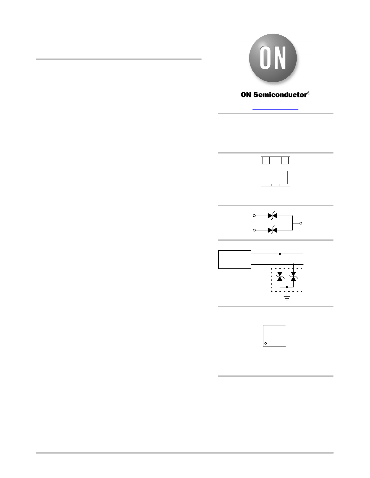
XDFNW3
DUAL BIDIRECTIONAL
VOLTAGE SUPPRESSOR
12
XDFNW3
CASE 521AC
PIN 1
PIN 2
CAN_H
CAN
Transceiver
CAN_L
MARKING DIAGRAM
24M
24 = Specific Device Code
M = Month Code
3
PIN 3
CAN Bus
SZNUP2124
© Semiconductor Components Industries, LLC, 2019
February, 2021 − Rev. 2
ORDERING INFORMATION
See detailed ordering and shipping information in the package
dimensions section on page 2 of this data sheet.
1 Publication Order Number:
SZNUP2124/D
Page 2

SZNUP2124
MAXIMUM RATINGS (T
Symbol
PPK Peak Power Dissipation
T
J
T
J
T
L
ESD Human Body Model (HBM)
8/20 ms Double Exponential Waveform (Note 1)
Operating Junction Temperature Range −55 to 175 °C
Storage Temperature Range −55 to 175 °C
Lead Solder Temperature (10 s) 260 °C
IEC 61000−4−2 Specification (Contact)
= 25°C, unless otherwise specified)
J
Rating Value Unit
120
16
28
W
kV
kV
Stresses exceeding those listed in the Maximum Ratings table may damage the device. If any of these limits are exceeded, device functionality
should not be assumed, damage may occur and reliability may be affected.
1. Non−repetitive current pulse per Figure 1.
ELECTRICAL CHARACTERISTICS (T
= 25°C, unless otherwise specified)
J
Symbol Parameter Test Conditions Min Typ Max Unit
V
RWM
V
V
I
CJ Capacitance VR = 0 V, f = 1 MHz (Line to GND)
DC
Reverse Working Voltage (Note 2) 24 V
Breakdown Voltage IT = 1 mA (Note 3) 26 27 33 V
BR
I
Reverse Leakage Current V
R
Clamping Voltage
C
Maximum Peak Pulse Current
PP
= 24 V 100 nA
RWM
IPP = 1 A (8/20 ms Waveform),
(Note 4)
8/20 ms Waveform (Note 4)
V
= 5 V, f = 1 MHz (Line to GND)
R
Diode Capacitance Matching VR = 0 V, f = 1 MHz (Note 5) 0.25 pF
40 V
3.0 A
10
6.0
pF
Product parametric performance is indicated in the Electrical Characteristics for the listed test conditions, unless otherwise noted. Product
performance may not be indicated by the Electrical Characteristics if operated under different conditions.
2. Surge protection devices are normally selected according to the working peak reverse voltage (V
than the DC or continuous peak operating voltage level.
is measured at pulse test current IT.
3. V
BR
4. Pulse waveform per Figure 1.
5. DC is the percentage difference between C
table.
of lines 1 and 2 measured according to the test condition given in the electrical characteristics
J
), which should be equal or greater
RWM
ORDERING INFORMATION
Device Part Orientation
SZNUP2124MXWTAG* Pin 1 − Upper Left
SZNUP2124MXWTBG* Pin 1 − Upper Right
†
Package Shipping
XDFNW3
(Pb−Free)
3,000 / Tape & Reel
†For information on tape and reel specifications, including part orientation and tape sizes, please refer to our Tape and Reel Packaging
Specifications Brochure, BRD8011/D.
*SZ Prefix for Automotive and Other Applications Requiring Unique Site and Control Change Requirements; AEC−Q101 Qualified and PPAP
Capable
†
www.onsemi.com
2
Page 3
SZNUP2124
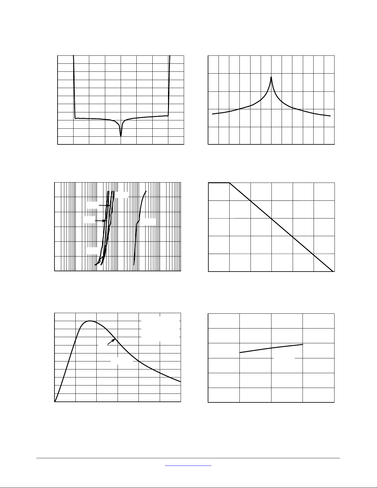
TYPICAL PERFORMANCE CURVES
(TJ = 25°C unless otherwise noted)
1E−02
1E−03
1E−04
1E−05
1E−06
1E−07
I (A)
1E−08
1E−09
1E−10
1E−11
1E−12
1E−13
−40 −30 −20 −10 0 10 20
V (V)
30 40
Figure 1. IV Characteristics
30
25
55°C
20
25°C
15
10
5
, REVERSE BIAS VOLTAGE (V)
R
V
0
1E−12 1E−10 1E−09 1E−071E−11 1E −08 1E−06
−55°C
IL, LEAKAGE CURRENT (A)
85°C
150°C
Figure 3. IR vs. Temperature Characteristics
10
8
6
C (pF)
4
2
0
−30 −25 −20 −15 −10 −5
0 5 10 15 20 25 30
V
(V)
BIAS
Figure 2. CV Characteristics
100
80
60
40
20
POWER DISSIPATION (%)
0
0 50 75 125 150
25 100
TEMPERATURE (°C)
Figure 4. Steady State Power Derating
110
100
90
80
70
60
50
40
30
20
% OF PEAK PULSE CURRENT
10
0
0 5 15 25
c−t
td = IPP/2
10 20
t, TIME (ms)
Figure 5. Pulse Waveform (8/20 ms)
WAVEFORM
PARAMETERS
= 8 ms
t
r
t
= 20 ms
d
www.onsemi.com
30
60
50
40
(V)
30
CLAMP
V
20
10
0
01234
I
PP
IO−GND
(A)
Figure 6. Clamping Voltage vs. Peak Pulse Current
(8/20 ms)
3
Page 4
SZNUP2124
TYPICAL PERFORMANCE CURVES
(TJ = 25°C unless otherwise noted)
100
80
60
40
VOLTAGE (V)
20
0
−20
140
120100806040200−20
TIME (ns) TIME (ns)
180160 200 180160 200
Figure 7. IEC61000−4−2 +8 kV Contact ESD
Clamping Voltage
20
0
−20
−40
VOLTAGE (V)
−60
−80
−100
140
120100806040200−20
Figure 8. IEC61000−4−2 −8 kV Contact ESD
Clamping Voltage
www.onsemi.com
4
Page 5

SZNUP2124
IEC 61000−4−2 Spec.
Test Volt-
Level
age (kV)
1 2 7.5 4 2
2 4 15 8 4
3 6 22.5 12 6
4 8 30 16 8
ESD Gun
First Peak
Current
(A)
Current at
30 ns (A)
Device
Under
Test
50 W
Cable
IEC61000−4−2 Waveform
I
peak
Current at
60 ns (A)
100%
90%
I @ 30 ns
I @ 60 ns
10%
Figure 9. IEC61000−4−2 Spec
Oscilloscope
50 W
tP = 0.7 ns to 1 ns
Figure 10. Diagram of ESD Clamping Voltage Test Setup
The following is taken from Application Note
AND8308/D − Interpretation of Datasheet Parameters
for ESD Devices.
ESD Voltage Clamping
For sensitive circuit elements it is important to limit the
voltage that an IC will be exposed to during an ESD event
to as low a voltage as possible. The ESD clamping voltage
is the voltage drop across the ESD protection diode during
an ESD event per the IEC61000−4−2 waveform. Since the
IEC61000−4−2 was written as a pass/fail spec for larger
systems such as cell phones or laptop computers it is not
clearly defined in the spec how to specify a clamping voltage
at the device level. ON Semiconductor has developed a way
to examine the entire voltage waveform across the ESD
protection diode over the time domain of an ESD pulse in the
form of an oscilloscope screenshot, which can be found on
the datasheets for all ESD protection diodes. For more
information on how ON Semiconductor creates these
screenshots and how to interpret them please refer to
AND8307/D.
www.onsemi.com
5
Page 6

SZNUP2124
20
18
16
14
12
10
8
6
TLP CURRENT (A)
4
2
0
0403010 20
VOLTAGE (V)
Figure 11. Positive TLP IV Curve
NOTE: TLP parameter: Z0 = 50 W, tp = 100 ns, tr = 300 ps, averaging window: t1 = 30 ns to t2 = 60 ns.
Transmission Line Pulse (TLP) Measurement
Transmission Line Pulse (TLP) provides current versus
10
8
(kV)
IEC
6
4
TLP CURRENT (A)
EQUIVALENT V
2
0
50
−20
−18
−16
−14
−12
−10
−8
−6
−4
−2
0
0403010 20 50
VOLTAGE (V)
Figure 12. Negative TLP IV Curve
L
voltage (I−V) curves in which each data point is obtained
from a 100 ns long rectangular pulse from a charged
transmission line. A simplified schematic of a typical TLP
50 W Coax
Cable
10 MW
system is shown in Figure 13. TLP I−V curves of ESD
protection devices accurately demonstrate the product’s
ESD capability because the 10s of amps current levels and
V
under 100 ns time scale match those of an ESD event. This
is illustrated in Figure 14 where an 8 kV IEC 61000−4−2
current waveform is compared with TLP current pulses at
Figure 13. Simplified Schematic of a Typical TLP
8 A and 16 A. A TLP I−V curve shows the voltage at which
the device turns on as well as how well the device clamps
voltage over a range of current levels.
S
C
System
Attenuator
÷
I
M
Oscilloscope
50 W Coax
Cable
V
M
DUT
10
8
6
4
2
0
(kV)
IEC
EQUIVALENT V
Figure 14. Comparison Between 8 kV IEC 61000−4−2 and 8 A and 16 A TLP Waveforms
www.onsemi.com
6
Page 7

SZNUP2124
APPLICATIONS
Background
The Controller Area Network (CAN) is a serial
communication protocol designed for providing reliable
high speed data transmission in harsh environments. surge
protection diodes provide a low cost solution to conducted
and radiated Electromagnetic Interference (EMI) and
Electrostatic Discharge (ESD) noise problems. The noise
bidirectional surge protection device in a compact
XDFNW3 package. This device is based on
Zener technology that optimizes the active area of a PN
junction to provide robust protection against transient EMI
surge voltage and ESD. The SZNUP2124 has been tested to
EMI and ESD levels that exceed the specifications of
popular high speed CAN and CAN−FD networks.
immunity level and reliability of CAN transceivers can be
easily increased by adding external surge protection diodes
to prevent transient voltage failures.
The SZNUP2124 provides a surge protection solution for
CAN data communication lines. The SZNUP2124 is a dual
Table 1. Transceiver Requirements for High−Speed CAN Networks
Parameter ISO 11898−2
Min / Max Bus Voltage
(12 V System)
Common Mode Bus Voltage CAN_L:
Transmission Speed 1.0 Mb/s @ 40 m
ESD Not specified, recommended w $8.0 kV (contact)
EMI Immunity ISO 7637−3, pulses ‘a’ and ‘b’
Popular Applications Automotive, Truck, Medical and Marine Systems
CAN Physical Layer Requirements
Table 1 provides a summary of the system requirements
for a CAN transceiver. The ISO 11898−2 physical layer
specification forms the baseline for most CAN systems.
−3.0 V / 16 V
−2.0 V (min)
2.5 V (nom)
CAN_H:
2.5 V (nom)
7.0 V (max)
125 kb/s @ 500 m
www.onsemi.com
7
Page 8

SZNUP2124
EMI Specifications
The EMI protection level provided by the surge protection
device can be measured using the International Organization
for Standardization (ISO) 7637−2 and −3 specifications that
are representative of various noise sources. The ISO 7637−2
specification is used to define the susceptibility to coupled
transient noise on a 12 V power supply, while ISO 7637−3
defines the noise immunity tests for data lines. The ISO 7637
tests also verify the robustness and reliability of a design by
applying the surge voltage for extended durations.
The IEC 61000−4−X specifications can also be used to
quantify the EMI immunity level of a CAN system. The IEC
61000−4 and ISO 7637 tests are similar; however, the IEC
standard was created as a generic test for any electronic
system, while the ISO 7637 standard was designed for
vehicular applications. The IEC61000−4−4 Electrical Fast
Transient (EFT) specification is similar to the ISO 7637−3
pulse 3a and b tests and is a requirement of SDS CAN
systems. The IEC 61000−4−5 test is used to define the power
absorption capacity of a surge protection device and long
duration voltage transients such as lightning. Table 2
provides a summary of the ISO 7637 and IEC 61000−4−X
test specifications. Table 3 provides the SZNUP2124’s ESD
test results.
Table 2. ISO 7637 and IEC 61000−4−X Test Specifications
Test Waveform Test Specifications SZNUP2124 Results Simulated Noise Source
Vs = 0 to −100 V
I
= 10 A
max
Pulse 1
t
duration
= 5000 pulses
ISO 7637−2
12 V Power Supply Lines
(Note 2)
Pulse 2a
Vs = 0 to +50 V
coupled onto 14 V battery
I
= 10 A
max
t
= 5000 pulses
duration
Vs = −60 V
ISO 7637−3
Repetitive data line fast
transients (Note 3)
IEC 61000−4−4
Data Line EFT
IEC 61000−4−5
Pulse ‘a’
Pulse ‘b’
t
I
= 1.2 A
max
t
= 10 minutes
duration
Vs = +40 V
I
= 0.8 A
max
t
= 10 minutes
duration
V
open circuit
I
short circuit
(Level 4 = Severe Industrial
= 2.0 kV
= 40 A
Environment)
= 50 W, tr < 5.0 ns,
R
i
d_50%
f
V
= 50 ns, t
burst
t
t
duration
open circuit
I
short circuit
= 2.0 to 5.0 kHz,
repeat
R
i
= 15 ms,
burst
= 300 ms
= 1 minute
= 1.2/50 ms,
= 8/20 ms
= 50 W
1. DUT = device under test.
2. Test specifications were taken from ISO7637−2: 2004 version.
3. Test specifications were taken from ISO7637−3: 1995 version.
4. DUT was tested to ISO7637−2: 2004 pulse 3a,b specification for more rigorous test.
5. The EFT immunity level was measured with test limits beyond the IEC 61000−4−4 test, but with the more severe test conditions of
ISO 7637−3.
I
= 1.75 A
max
V
clamp_max
t
duration
= 10 W, tr = 1.0 ms,
R
i
= 2000 ms, t1 = 2.5 s,
t
d_10%
= 200 ms, t3 = 100 ms
t
2
V
clamp_max
t
duration
Ri = 2 W, t
t
d_10%
I
max
V
clamp_max
t
duration
= 50 W, tr = 5.0 ns,
R
i
= 100 ns, t1 = 100 ms,
t
d_10%
t
= 10 ms, t3 = 90 ms
2
= TBD V
= 5000 pulses
I
= 9.5 A
max
= TBD V
= 5000 pulses
= 1.0 ms,
r
= 50 ms, t1 = 2.5 s,
t
= 200 ms
2
= 50 A (Note 4)
= TBD V
= 60 minutes
(Note 5) Switching noise of inductive
I
= 8.0 A Lightning, nonrepetitive
max
DUT (Note 1) in parallel with
inductive load that is
disconnected from power
supply.
DUT in series with inductor
(wire harness) that is
disconnected from load.
Switching noise of inductive
loads.
loads.
power line and load
switching
www.onsemi.com
8
Page 9

SZNUP2124
Table 3. SZNUP2124 ESD Test Results
ESD Specification Test Test Level Pass / Fail
Human Body Model Contact 8 kV Pass
Contact 12.5 kV Pass
IEC 61000−4−2
Surge protection Diode Protection Circuit
ESD diodes provide protection to a transceiver by
clamping a surge voltage to a safe level. ESD diodes have
high impedance below and low impedance above their
breakdown voltage. An ESD diode has its junction
optimized to absorb the high peak energy of a transient
event, while a standard diode is designed and specified to
clamp a steady state voltage.
Figure 15 provides an example of a dual bidirectional
ESD diode array that can be used for protection with the
high−speed CAN network. The clamping voltage of the
composite device is equal to the breakdown voltage of the
diode that is reversed biased, plus the diode drop of the
second diode that is forwarded biased.
Non−contact (Air Discharge) 12.5 kV Pass
CAN_H
CAN
Transceiver
CAN_L
Figure 15. CAN ESD Circuit
CAN Bus
NUP2124L
www.onsemi.com
9
Page 10

SZNUP2124
PACKAGE DIMENSIONS
XDFNW3 1x1, 0.65P
CASE 521AC
ISSUE A
www.onsemi.com
10
Page 11

SZNUP2124
ON Semiconductor and are trademarks of Semiconductor Components Industries, LLC dba ON Semiconductor or its subsidiaries in the United States and/or other countries.
ON Semiconductor owns the rights to a number of patents, trademarks, copyrights, trade secrets, and other intellectual property. A listing of ON Semiconductor’s product/patent
coverage may be accessed at www.onsemi.com/site/pdf/Patent−Marking.pdf
ON Semiconductor makes no warranty, representation or guarantee regarding the suitability of its products for any particular purpose, nor does ON Semiconductor assume any liability
arising out of the application or use of any product or circuit, and specifically disclaims any and all liability, including without limitation special, consequential or incidental damages.
Buyer is responsible for its products and applications using ON Semiconductor products, including compliance with all laws, regulations and safety requirements or standards,
regardless of any support or applications information provided by ON Semiconductor. “Typical” parameters which may be provided in ON Semiconductor data sheets and/or
specifications can and do vary in different applications and actual performance may vary over time. All operating parameters, including “Typicals” must be validated for each customer
application by customer’s technical experts. ON Semiconductor does not convey any license under its patent rights nor the rights of others. ON Semiconductor products are not
designed, intended, or authorized for use as a critical component in life support systems or any FDA Class 3 medical devices or medical devices with a same or similar classification
in a foreign jurisdiction or any devices intended for implantation in the human body. Should Buyer purchase or use ON Semiconductor products for any such unintended or unauthorized
application, Buyer shall indemnify and hold ON Semiconductor and its officers, employees, subsidiaries, affiliates, and distributors harmless against all claims, costs, damages, and
expenses, and reasonable attorney fees arising out of, directly or indirectly, any claim of personal injury or death associated with such unintended or unauthorized use, even if such
claim alleges that ON Semiconductor was negligent regarding the design or manufacture of the part. ON Semiconductor is an Equal Opportunity/Affirmative Action Employer. This
literature is subject to all applicable copyright laws and is not for resale in any manner.
. ON Semiconductor reserves the right to make changes without further notice to any products herein.
PUBLICATION ORDERING INFORMATION
LITERATURE FULFILLMENT:
Email Requests to: orderlit@onsemi.com
ON Semiconductor Website: www.onsemi.com
◊
TECHNICAL SUPPORT
North American Technical Support:
Voice Mail: 1 800−282−9855 Toll Free USA/Canada
Phone: 011 421 33 790 2910
www.onsemi.com
Europe, Middle East and Africa Technical Support:
Phone: 00421 33 790 2910
For additional information, please contact your local Sales Representative
11
 Loading...