

ON Semiconductor MURHD560T4G, SURHD8560T4G, MURHD560W1T4G, SURHD8560W1T4G, SURHD8560T4G-VF01 User Manual
Page 1
MURHD560T4G,
,
SURHD8560T4G,
MURHD560W1T4G,
SURHD8560W1T4G,
SURHD8560T4G-VF01
600 V, 5 A Power Rectifier
Features and Benefits
• Ultrafast 30 Nanosecond Recovery Times
• 175°C Operating Junction Temperature
• High Temperature Glass Passivated Junction
• High Voltage Capability to 600 Volts
• SURHD8 Prefix for Automotive and Other Applications Requiring
Unique Site and Control Change Requirements; AEC−Q101
Qualified and PPAP Capable
• These Devices are Pb−Free, Halogen Free/BFR Free and are RoHS
Compliant
Applications
• Power Supplies
• Inverters
• Free Wheeling Diodes
Mechanical Characteristics
• Case: Epoxy, Molded
• Epoxy Meets UL 94 V−0 @ 0.125 in
• Weight: 0.4 g (approximately)
• Finish: All External Surfaces Corrosion Resistant and Terminal
Leads are Readily Solderable
• Lead Temperature for Soldering Purposes:
260°C Max. for 10 Seconds
• ESD Ratings:
♦ Machine Model = C (> 400 V)
♦ Human Body Model = 3B (> 8000 V)
www.onsemi.com
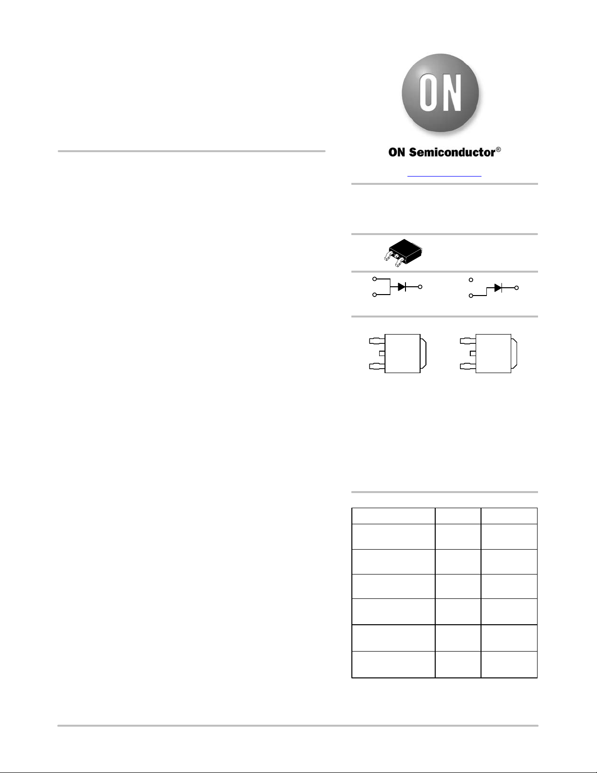
ULTRAFAST RECTIFIER
5.0 AMPERES
600 VOLTS
DPAK
CASE 369C
STYLES 3, 8
1
3
STYLE 3 STYLE 8
MARKING DIAGRAMS
AYWW
UH560G
STYLE 3 STYLE 8
UH560 = MURHD560T4
560W1 = MURHD560W1T4
A = Assembly Location
Y = Year
WW = Work Week
G = Pb−Free Package
* The Assembly Location code (A) is front side
optional. In cases where the Assembly Location is
stamped in the package bottom (molding ejecter
pin), the front side assembly code may be blank.
ORDERING INFORMATION
Device Package Shipping
MURHD560T4G DPAK
SURHD8560T4G DPAK
MURHD560W1T4G DPAK
SURHD8560W1T4G DPAK
4
1
3
(Pb−Free)
(Pb−Free)
(Pb−Free)
(Pb−Free)
AYWW
560W1G
2,500 /
Tape & Reel
2,500 /
Tape & Reel
2,500 /
Tape & Reel
2,500 /
Tape & Reel
4
†
© Semiconductor Components Industries, LLC, 2016
June, 2017 − Rev. 10
SSURHD8560W1T4G DPAK
SSURHD8560T4G−
VF01
†For information on tape and reel specifications,
including part orientation and tape sizes, please
refer to our Tape and Reel Packaging Specification
Brochure
1 Publication Order Number:
BRD8011/D.
(Pb−Free)
DPAK
(Pb−Free)
2,500 /
Tape & Reel
2,500 /
Tape & Reel
MURHD560/D
Page 2
MURHD560T4G, SURHD8560T4G, MURHD560W1T4G, SURHD8560W1T4G,
MAXIMUM RATINGS
Rating Symbol Value Unit
Peak Repetitive Reverse Voltage
Working Peak Reverse Voltage
DC Blocking Voltage
Average Rectified Forward Current
(Rated V
, TC = 159°C)
R
Non−Repetitive Peak Surge Current
(Surge Applied at Rated Load Conditions Halfwave, Single Phase, 60 Hz)
Operating Junction and Storage Temperature Range TJ, T
Stresses exceeding those listed in the Maximum Ratings table may damage the device. If any of these limits are exceeded, device functionality
should not be assumed, damage may occur and reliability may be affected.
THERMAL CHARACTERISTICS
Rating Symbol Value Unit
Maximum Thermal Resistance, Junction to Case
Maximum Thermal Resistance, Junction to Ambient (Note 1)
1. Rating applies when surface mounted on a 1.5 mm FR4 PC board with a 1 oz. thick, 700 mm2 Cu area.
ELECTRICAL CHARACTERISTICS
Rating Symbol Value Unit
Maximum Instantaneous Forward Voltage (Note 2)
(I
= 5.0 Amps, TC = 25°C)
F
(IF = 5.0 Amps, TC = 125°C)
Maximum Instantaneous Reverse Current (Note 2)
(Rated dc Voltage, T
(Rated dc Voltage, TC = 125°C)
Maximum Reverse Recovery Time
= 1.0 Amp, di/dt = 50 Amps/ms, VR = 30 V, TJ = 25°C)
(I
F
Product parametric performance is indicated in the Electrical Characteristics for the listed test conditions, unless otherwise noted. Product
performance may not be indicated by the Electrical Characteristics if operated under different conditions.
2. Pulse Test: Pulse Width = 300 ms, Duty Cycle ≤ 2.0%.
= 25°C)
C
V
V
RWM
I
F(AV)
I
FSM
R
R
RRM
V
R
q
JC
q
JA
V
F
I
R
t
rr
stg
600 V
A
5.0
A
50
−65 to +175 °C
2.5 °C/W
49.5 °C/W
V
2.7
1.65
mA
10
70
ns
30
www.onsemi.com
2
Page 3

MURHD560T4G, SURHD8560T4G, MURHD560W1T4G, SURHD8560W1T4G,
0
100
10
125°C
1
0.1
, FORWARD CURRENT (AMPS)
F
0.01
0
V
, INSTANTANEOUS FORWARD VOLTAGE (VOLTS)
F
Figure 1. Typical Forward Voltage Figure 2. Maximum Forward Voltage
1.0E−4
1.0E−5
1.0E−6
150°C
100°C
25°C
1.50.5 3.0
2.01.0
2.5
150°C
125°C
100°C
100
10
150°C
125°C
1
0.1
, FORWARD CURRENT (AMPS)
F
I
0.01
0
V
, MAXIMUM FORWARD VOLTAGE (VOLTS)
F
1.0E−3
1.0E−4
1.0E−5
25°C
100°C
3.01.0 6.0
4.02.0
5.0
150°C
125°C
100°C
1.0E−7
1.0E−8
, REVERSE CURRENT (AMPS) I
R
I
1.0E−9
100
90
80
70
60
50
40
30
C, CAPACITANCE (pF)
20
10
0
0
1.0E−6
25°C
100 200 300
, REVERSE VOLTAGE (VOLTS)
V
R
400
500
1.0E−7
1.0E−8
, MAXIMUM REVERSE CURRENT (AMPS)
R
6000
0
I
100 200 300
VR, REVERSE VOLTAGE (VOLTS)
25°C
400
Figure 3. Typical Reverse Current Figure 4. Maximum Reverse Current
20
TJ = 175°C
15
SQUARE
WAVE
dc
524 6
12525 75 175
, REVERSE VOLTAGE (VOLTS)
V
R
15050 100 200
(WATTS)
, AVERAGE POWER DISSIPATION
FO
P
10
5
0
10
37
IO, AVERAGE FORWARD CURRENT (AMPS)
500
60
8
Figure 5. Typical Capacitance Figure 6. Forward Power Dissipation
www.onsemi.com
3
Page 4

MURHD560T4G, SURHD8560T4G, MURHD560W1T4G, SURHD8560W1T4G,
9
8
7
6
SQUARE WAVE
5
4
3
2
1
0
, AVERAGE FORWARD CURRENT (AMPS)
F
I
120 150100
110 140
, CASE TEMPERATURE (°C)
T
C
Figure 7. Current Derating
10
0.5
1
0.2
0.1
0.05
0.01
0.1
Single Pulse
, TRANSIENT THERMAL RESISTANCE
0.01
(t)
R
0.00001 100
R
dc
= 2.5°C/W
q
JC
= 175°C
T
J
130 170160 180
0.0001 0.001 0.01 1.0 10
Figure 9. Thermal Response, Junction to Case
, NON-REPETITIVE SURGE CURRENT (A)
I
t, TIME (s)
10,000
1,000
100
FSM
10
10
100 10,000
, SQUARE WAVE PULSE DURATION (ms)
t
p
1,000
Figure 8. Typical Non−Repetitive Surge
Current
* Typical performance based on a limited sample size. ON Semiconductor
does not guarantee ratings not listed in the Maximum Ratings table.
P
(pk)
t
1
t
2
DUTY CYCLE, D = t1/t
2
10000.10.000001
100
0.1
, TRANSIENT THERMAL RESISTANCE
0.01
(t)
R
10
1
0.5
0.2
0.1
0.05
0.01
Single Pulse
0.00001 100
0.0001 0.001 0.01 1.0 10
t, TIME (s)
Figure 10. Thermal Response, Junction to Ambient
www.onsemi.com
4
P
(pk)
t
1
t
2
DUTY CYCLE, D = t1/t
2
10000.10.000001
Page 5

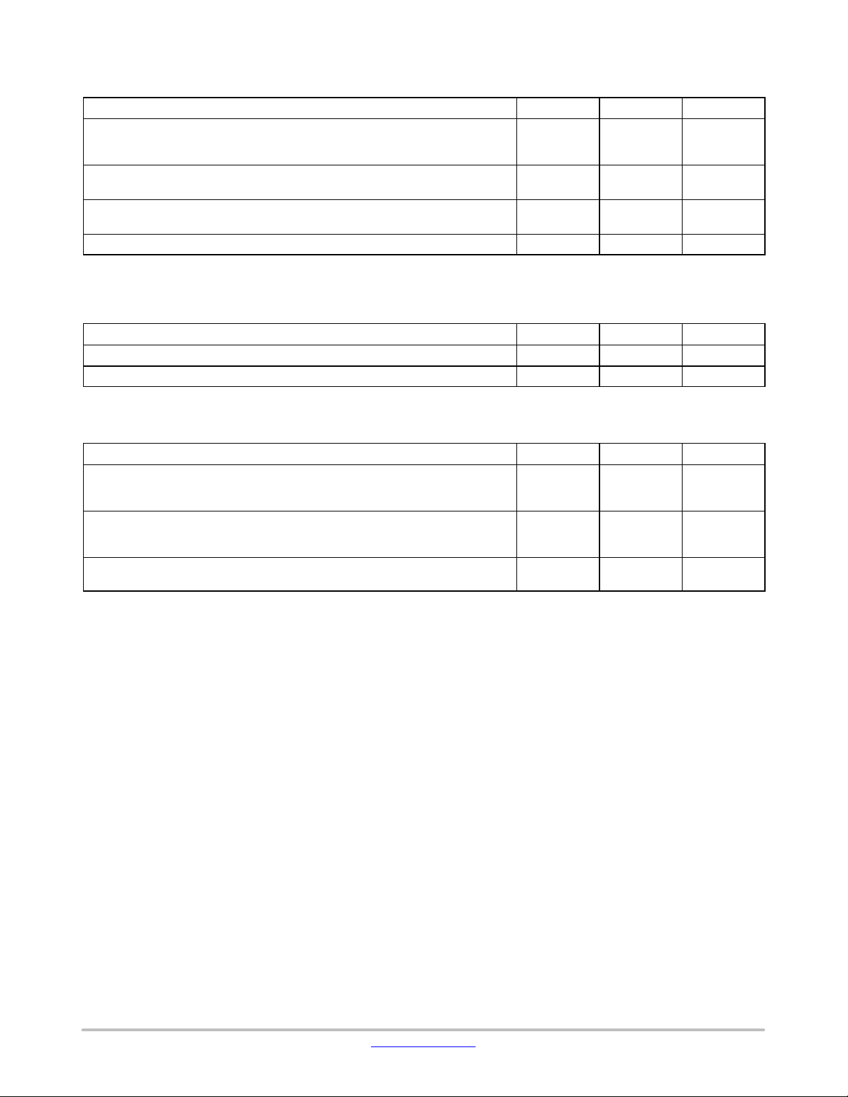
MECHANICAL CASE OUTLINE
PACKAGE DIMENSIONS
2
1
3
SCALE 1:1
L3
L4
b2
GAUGE
L2
PLANE
STYLE 1:
PIN 1. BASE
2. COLLECTOR
3. EMITTER
4. COLLECTOR
STYLE 6:
PIN 1. MT1
2. MT2
3. GATE
4. MT2
4
12 3
e
TOP VIEW
L
DETAIL A
ROTATED 90 CW5
STYLE 7:
PIN 1. GATE
5.80
0.228
E
A
b3
4
B
D
NOTE 7
b
0.005 (0.13) C
M
H
SEATING
C
PLANE
L1
2. COLLECTOR
3. EMITTER
4. COLLECTOR
A1
STYLE 2:
PIN 1. GATE
2. DRAIN
3. SOURCE
4. DRAIN
STYLE 8:
PIN 1. N/C
2. CATHODE
3. ANODE
4. CATHODE
STYLE 3:
SOLDERING FOOTPRINT*
6.20
0.244
2.58
0.102
DETAIL A
c
SIDE VIEW
PIN 1. ANODE
2. CATHODE
3. ANODE
4. CATHODE
3.00
0.118
1.60
0.063
DPAK (SINGLE GAUGE)
CASE 369C
ISSUE F
C
A
c2
H
BOTTOM VIEW
Z
BOTTOM VIEW
ALTERNATE
CONSTRUCTIONS
STYLE 4:
PIN 1. CATHODE
2. ANODE
3. GATE
4. ANODE
STYLE 9:
PIN 1. ANODE
2. CATHODE
3. RESISTOR ADJUST
4. CATHODE
6.17
0.243
STYLE 5:
PIN 1. GATE
2. ANODE
3. CATHODE
4. ANODE
STYLE 10:
PIN 1. CATHODE
2. ANODE
3. CATHODE
4. ANODE
DATE 21 JUL 2015
NOTES:
1. DIMENSIONING AND TOLERANCING PER ASME
Y14.5M, 1994.
2. CONTROLLING DIMENSION: INCHES.
3. THERMAL PAD CONTOUR OPTIONAL WITHIN DIMENSIONS b3, L3 and Z.
4. DIMENSIONS D AND E DO NOT INCLUDE MOLD
FLASH, PROTRUSIONS, OR BURRS. MOLD
FLASH, PROTRUSIONS, OR GATE BURRS SHALL
Z
Z
NOT EXCEED 0.006 INCHES PER SIDE.
5. DIMENSIONS D AND E ARE DETERMINED AT THE
OUTERMOST EXTREMES OF THE PLASTIC BODY.
6. DATUMS A AND B ARE DETERMINED AT DATUM
PLANE H.
7. OPTIONAL MOLD FEATURE.
DIM MIN MAX MIN MAX
A 0.086 0.094 2.18 2.38
A1 0.000 0.005 0.00 0.13
b 0.025 0.035 0.63 0.89
b2 0.028 0.045 0.72 1.14
b3 0.180 0.215 4.57 5.46
c 0.018 0.024 0.46 0.61
c2 0.018 0.024 0.46 0.61
D 0.235 0.245 5.97 6.22
E 0.250 0.265 6.35 6.73
e 0.090 BSC 2.29 BSC
H 0.370 0.410 9.40 10.41
L 0.055 0.070 1.40 1.78
L1 0.114 REF 2.90 REF
L2 0.020 BSC 0.51 BSC
L3 0.035 0.050 0.89 1.27
L4 −−− 0.040 −−− 1.01
Z 0.155 −−− 3.93 −−−
MILLIMETERSINCHES
GENERIC
MARKING DIAGRAM*
XXXXXXG
ALYWW
XXXXXX = Device Code
A = Assembly Location
L = Wafer Lot
Y = Year
WW = Work Week
G = Pb−Free Package
*This information is generic. Please refer
to device data sheet for actual part
marking.
AYWW
XXX
XXXXXG
DiscreteIC
mm
ǒ
SCALE 3:1
inches
Ǔ
*For additional information on our Pb−Free strategy and soldering
details, please download the ON Semiconductor Soldering and
Mounting Techniques Reference Manual, SOLDERRM/D.
DOCUMENT NUMBER:
DESCRIPTION:
ON Semiconductor and are trademarks of Semiconductor Components Industries, LLC dba ON Semiconductor or its subsidiaries in the United States and/or other countries.
ON Semiconductor reserves the right to make changes without further notice to any products herein. ON Semiconductor makes no warranty, representation or guarantee regarding
the suitability of its products for any particular purpose, nor does ON Semiconductor assume any liability arising out of the application or use of any product or circuit, and specifically
disclaims any and all liability, including without limitation special, consequential or incidental damages. ON Semiconductor does not convey any license under its patent rights nor the
rights of others.
© Semiconductor Components Industries, LLC, 2018
98AON10527D
DPAK (SINGLE GAUGE)
Electronic versions are uncontrolled except when accessed directly from the Document Repository.
Printed versions are uncontrolled except when stamped “CONTROLLED COPY” in red.
PAGE 1 OF 1
www.onsemi.com
Page 6

ON Semiconductor and are trademarks of Semiconductor Components Industries, LLC dba ON Semiconductor or its subsidiaries in the United States and/or other countries.
ON Semiconductor owns the rights to a number of patents, trademarks, copyrights, trade secrets, and other intellectual property. A listing of ON Semiconductor’s product/patent
coverage may be accessed at www.onsemi.com/site/pdf/Patent−Marking.pdf
ON Semiconductor makes no warranty, representation or guarantee regarding the suitability of its products for any particular purpose, nor does ON Semiconductor assume any liability
arising out of the application or use of any product or circuit, and specifically disclaims any and all liability, including without limitation special, consequential or incidental damages.
Buyer is responsible for its products and applications using ON Semiconductor products, including compliance with all laws, regulations and safety requirements or standards,
regardless of any support or applications information provided by ON Semiconductor. “Typical” parameters which may be provided in ON Semiconductor data sheets and/or
specifications can and do vary in different applications and actual performance may vary over time. All operating parameters, including “Typicals” must be validated for each customer
application by customer’s technical experts. ON Semiconductor does not convey any license under its patent rights nor the rights of others. ON Semiconductor products are not
designed, intended, or authorized for use as a critical component in life support systems or any FDA Class 3 medical devices or medical devices with a same or similar classification
in a foreign jurisdiction or any devices intended for implantation in the human body. Should Buyer purchase or use ON Semiconductor products for any such unintended or unauthorized
application, Buyer shall indemnify and hold ON Semiconductor and its officers, employees, subsidiaries, affiliates, and distributors harmless against all claims, costs, damages, and
expenses, and reasonable attorney fees arising out of, directly or indirectly, any claim of personal injury or death associated with such unintended or unauthorized use, even if such
claim alleges that ON Semiconductor was negligent regarding the design or manufacture of the part. ON Semiconductor is an Equal Opportunity/Affirmative Action Employer. This
literature is subject to all applicable copyright laws and is not for resale in any manner.
. ON Semiconductor reserves the right to make changes without further notice to any products herein.
PUBLICATION ORDERING INFORMATION
LITERATURE FULFILLMENT:
Email Requests to: orderlit@onsemi.com
ON Semiconductor Website: www.onsemi.com
TECHNICAL SUPPORT
North American Technical Support:
Voice Mail: 1 800−282−9855 Toll Free USA/Canada
Phone: 011 421 33 790 2910
Europe, Middle East and Africa Technical Support:
Phone: 00421 33 790 2910
For additional information, please contact your local Sales Representative
◊
www.onsemi.com
1
 Loading...