Page 1

SECO-HVDCDC1362-15W15V
L
B
C
-GEVB
15 W SiC High-Voltage
Auxiliary Power Supply for
HEV & BEV Applications
Evaluation Board User's
Manual
Introduction
SECO−HVDCDC1362−15W15V−GEVB is highly efficient and
primary−side regulated (PSR) auxiliary power supply targeting HEV
and EV automotive power trains. The design provides a stable 15 V
output and 15 W over a wide input DC voltage range from 250 V to
900 V, and is therefore suitable for 400 V and 800 V battery systems.
The board employs the NCV1362 quasi−resonant peak current PSR
flyback controller, the 3−lead cost−optimized NVHL160N120SC1
160 mW 1200 V silicon carbide (SiC) MOSFET, and the
FFSD0665B−F085 SiC diode.
Thanks to the high blocking voltage capabilities and ultra−low gate
charge (34 nC) value of the SiC FET, the switching losses are
significantly reduced, and the board exhibits a superior efficiency for
the application up to 86% in low line input conditions. The notable
driving capabilities of the NCV1362 controller allows for direct
operation of the SiC FET at 12V without a pre−driver, simplifying the
layout and cutting down the component count.
The flyback transformer provides 4 kV isolation and is optimized to
minimize the losses on the RCD snubber. Consequently the system
effectively dampens the drain voltage overshoot at high line, and
provides 100 V margin for the SiC FET. The board is fully realized
with automotive qualified semiconductors and passive devices.
Industrial grade replacements are also available.
www.onsemi.com
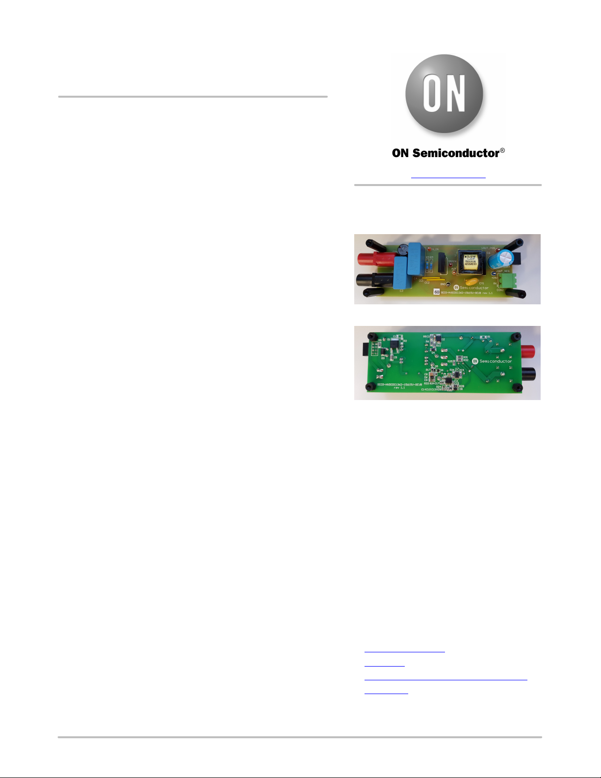
EVAL BOARD USER’S MANUA
(Top View)
(Bottom View)
Figure 1. Board Layout
Features
• NCV1362 (Automotive) / NCP1362 (Industrial) Quasi−resonant
Peak Current PSR Flyback Controller
• Fully Automotive Qualified Devices
• Vin = 240 V – 900 V DC Only
• Vout = 15 V / 15 W Continuous
• Electromagnetic Compatibility (EN 55015 Limits)
• High Efficiency up to 86%
• SiC FET Directly Operated at 12 V by the IC
• Excellent Thermal Performance
Applications
• HEV & EV Vehicles Auxiliary Power Supplies
• Automotive Powertrain Systems
• EV Charging and DC−DC Conversion
enefits
• Superior Efficiency with SiC Devices
• Stable Performance across a Wide Input
Voltage Range (250 Vdc – 900 Vdc )
• Reduced Bill−of−Material and
Cost−optimized
• Fully AEC−Q Qualified Parts
• EMC within EN 55015 Limits
• Single Layer PCB
ollateral
• NVHL160N120SC1
• NCV1362
• SECO−HVDCDC1362−15W15V−GEVB
• References
• Industrial DC−DC Conversion, Solar Inverts (with Industrial grade)
© Semiconductor Components Industries, LLC, 2020
October, 2020 − Rev. 1
1 Publication Order Number:
EVBUM2752/D
Page 2

SECO−HVDCDC1362−15W15V−GEVB
Scope and Purpose
The purpose of this user’s manual is to present the design
of an auxiliary power supply with automotive qualified parts
NCV1362 (NCP1362) and NVHL160N120SC1 SiC FET.
The design was tested as described in this document but not
System Overview
qualified regarding safety requirements or manufacturing
and operation over the complete operating temperature
range or lifetime. The hardware is intended for testing under
laboratory conditions and by trained specialists only.
Block Diagram
Figure 2. Evaluation Board Photo
Figure 3. Block Diagram
www.onsemi.com
2
Page 3

SECO−HVDCDC1362−15W15V−GEVB
SPECIFICATION
Parameters
Values
Input
Voltage
250−900 VDC
Current
71 mA (Vin = 250 V), 22 mA (Vin = 900 V)
Output
Power
15 W
Voltage
15 VDC
Current per branch
1 A
Total current
1 A
Efficiency at full load
86% (Vin = 250 V)
Temperature at full load
98°C (Vin = 6 V), 74.5°C (Vin = 15 V), 76°C (Vin = 18 V)
Control
Core part
NCV1362
Topology
Flyback
Switching frequency
50 kHz
Operation mode
DCM
Primary side peak current
0.65 A
Construction
Board size
26.24 x 16.38 x 16.06 mm
Transformer
Dielectric insulation
4000 VAC, 1 min.
Inductance
1.70 mH ± 10%
Leakage inductance
20 mH typ. / 40 mH max.
Safety standard
IEC62368−1
Pollution degree
1
Application
HEV & EV vehicles, automotive powertrain systems, EV charging and DC−DC conversion
www.onsemi.com
3
Page 4

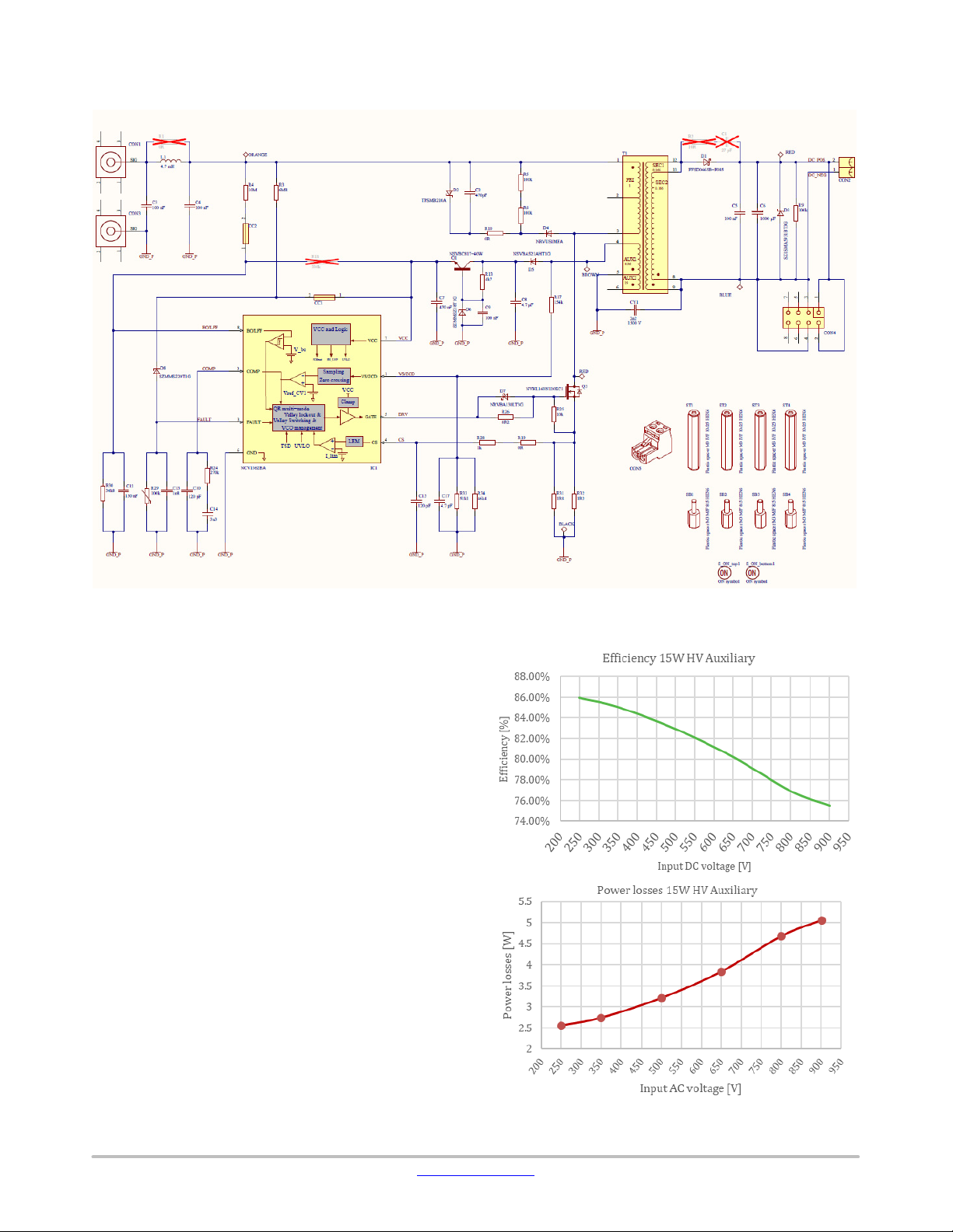
Schematic
SECO−HVDCDC1362−15W15V−GEVB
Figure 4. Evaluation Board Schematic
TEST REPORT
This section presents the results of the tests conducted on
the power supply.
• Efficiency DC/DC at input voltage range and full load
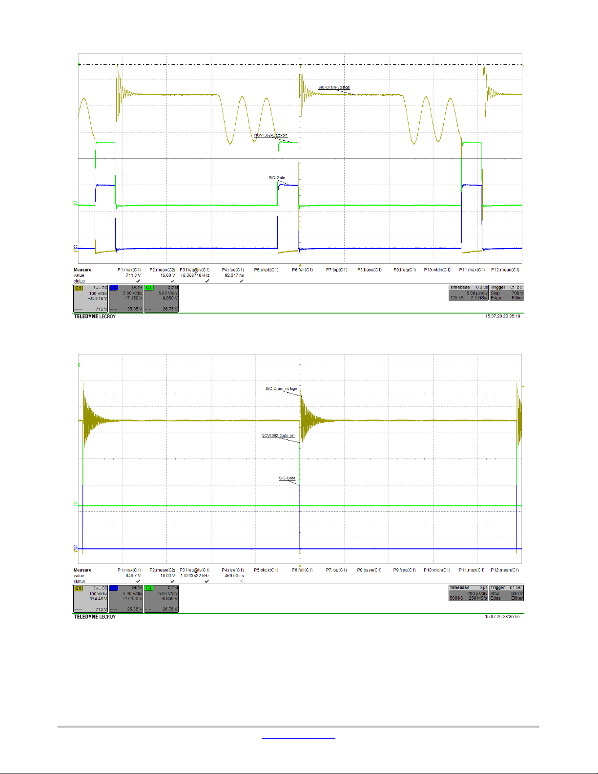
• Waveforms at 240V, 500V, 900V at full load / open
circuit
• Load transients 15%−85% and 15%−85% load
• Thermal camera view
• Electromagnetic compatibility
Efficiency DC/DC at Input Voltage Range and Full Load
Measured conditions:
• Output power Pout ~ 15 W
• Electronic load: Chroma 6147A used channel 3 as CRH
(constant resistance high mode 15 W → 1.0 A)
List of equipment:
• DC source: Magna−Power 0−1000V
• Power analyzer: Textronix PA3000
• Electronic load: Chroma
www.onsemi.com
4
Figure 5.
Page 5

SECO−HVDCDC1362−15W15V−GEVB
Waveforms at 240 V, 500 V, 900 V at Full Load / Open
Circuit
Measured conditions:
• Output power Pout ~ 15 W
• Electronic load: Chroma 6147A used channel 3 as CRH
(constant resistance high mode 15 Ohm −> 1.0A)
List of equipment:
• DC source: Magna−Power 0−1000V
• Power analyzer: Textronix PA3000
• Electronic load: Chroma
• Oscilloscope: Lecroy HDO8038
Figure 6. 250 V DC Full Load
Figure 7. 250 V DC Open Circuit
www.onsemi.com
5
Page 6

SECO−HVDCDC1362−15W15V−GEVB
Figure 8. 500 V DC Full Load
Figure 9. 500 V DC Open Circuit
www.onsemi.com
6
Page 7

SECO−HVDCDC1362−15W15V−GEVB
Figure 10. 900 V DC Full Load
Figure 11. 900 V DC Open Circuit
www.onsemi.com
7
Page 8

SECO−HVDCDC1362−15W15V−GEVB
Load Transients 15%−85% and 15%−85% Load
Measured conditions:
• Output power Pout ~ 15 W
• Electronic load: Chroma 6147A used channel 3 as
CCDL (constant current dynamic mode 0.15 A →
0.85 A)
List of equipment:
• DC source: Magna−Power 0−1000V
• Power analyzer: Textronix PA3000
• Electronic load: Chroma
• Oscilloscope: Lecroy HDO8038
Figure 12. 250 V − 15% to 85%
Figure 13. 250 V − 85% to 15%
www.onsemi.com
8
Page 9

SECO−HVDCDC1362−15W15V−GEVB
Figure 14. 500 V − 15% to 85%
Figure 15. 500 V − 85% to 15%
www.onsemi.com
9
Page 10

SECO−HVDCDC1362−15W15V−GEVB
Figure 16. 900 V − 15% to 85%
Figure 17. 900 V − 85% to 15%
www.onsemi.com
10
Page 11

SECO−HVDCDC1362−15W15V−GEVB
Thermal Camera View
Measured conditions:
• Output power Pout ~ 15 W
• Electronic load: Chroma 6147A used channel 3 as CRH
(constant resistance high mode 15 W → 1.0 A)
• Input voltage ~ 900 V DC
• After 5 minutes in this conditions
Sp1 − Transformer
Sp2 – SiC switcher
Sp3 – Startup high voltage resistor
Sp1 – Secondary rectifier
Sp2 – IC NCV 1362
Sp3 – Snubber TVS diode
Figure 18.
www.onsemi.com
11
Page 12

SECO−HVDCDC1362−15W15V−GEVB
Measured conditions:
• Output power Pout ~ 15 W
• Electronic load: Chroma 6147A used channel 3 as CRH
(constant resistance high mode 15 W → 1.0 A)
Sp1 − Transformer
Sp2 – SiC switcher
Sp3 – Startup high voltage resistor
• Input voltage ~ 250 V DC
• After 5 minutes in this conditions
Sp1 – Secondary rectifier
Sp2 – IC NCV 1362
Sp3 – Snubber TVS diode
Figure 19.
www.onsemi.com
12
Page 13

SECO−HVDCDC1362−15W15V−GEVB
Electromagnetic Compatibility – Conducted Emissions
EN55015 Limits
Measured conditions:
• Output power Pout ~ 18 W resistive load
• Input voltage ~ 250 V
Figure 20.
www.onsemi.com
13
Page 14

Transformer Design
SECO−HVDCDC1362−15W15V−GEVB
Figure 21. Drawing and Parameters of Used Transformer
www.onsemi.com
14
Page 15

SECO−HVDCDC1362−15W15V−GEVB
Table 1. BILL OF MATERIAL
Des.
Comment
Description
Manufacturer
Manufacturer Part Number
C2
470pF
MLC capacitor 470pF 1kV ±10% X7R Würth Elek-
Würth Electronik
885342208017
C3, C4
100 nF
MMKT film capacitor 100n 500Vac/1600Vdc TDK
TDK
B32643B1104J000
C5
100 nF
Multilayer Ceramic Capacitors MLCC − SMD 1206
Murata
GRT31C5C1E104FA02
C6
1000 mF
ALU electrolyte high current ripple 1000 mF 25 V
NICHICON
UBT1E102MHD1TO
C7
470 nF
Multilayer Ceramic Capacitors MLCC − SMD 0805
Murata
GRT21BR71H474KE01
C8
4.7 mF
Multilayer Ceramic Capacitors MLCC − SMD 1210
Murata
GRT32ER71H475KE01
C9
100 nF
Multilayer Ceramic Capacitors MLCC − SMD 1206
Murata
GRT31C5C1H104JA02
C10, C15
120 pF
Multilayer Ceramic Capacitors MLCC − SMD 0603
Murata
GRT1885C2A121JA02
C12
150 nF
Multilayer Ceramic Capacitors MLCC − SMD 0603
Murata
GRT188R71E154KE01
C13
1n8
Multilayer Ceramic Capacitors MLCC − SMD 0805
Murata
GRT2165C2A182JA02
C14
3n3
Multilayer Ceramic Capacitors MLCC − SMD 0805
Murata
GRT2165C2A332JA02
C17
4.7 pF
Multilayer Ceramic Capacitors MLCC − SMD 0603
Murata
GCM1885C2A4R7CA16D
CON1
RED
Banana Test Connector, 4mm, Receptacle, PCB
CLIFF
FCR7350R
CON2
691 313 510
PCB right angle connector 2 pins 5.08 mm pitch
Würth Elektronik
691313510002
CON3
BLACK
Banana Test Connector, 4mm, Receptacle, PCB
CLIFF
FCR7350B
CON4
613 008 243
WR−PHD 2.54 mm Angled Dual Socket Header
Würth Elektronik
613008243121
CON5
691 351 500
Cable connector series 351 2pins 5.08 mm Würth
Würth Elektronik
691351500002
CY1
2n2
Disc ceramic capacitor 2n2 1500 VDC Y5U 10 %
VISHAY
AY1222M47Y5UC63L0
D1
FFSD0665B
Ultra fast Schottky SiC diode 650V 6A AEC−Q101
ON
FFSD0665B−F085
D2
TPSMB210A
TVS 210V 600W SMB unidirectional Littelfuse
Littelfuse
TPSMB210A
D3
SZ1SMA593
TVS zener diode 18 V 83 mA SMA AEC−Q101
ON
SZ1SMA5931BT3G
D4
NRVUS1MF
Super Fast diode 1000 V 1 A 75 ns SOD123FA
ON
NRVUS1MFA
D5
NSVBAS21A
Switching diode 250V 200mA SOD323 AEC−Q101
ON
NSVBAS21AHT1G
D6
SZMMSZ18
Zener Single Diode, 18 V, 500 mW, SOD−123, 5 %,
ON
SZMMSZ18T1G
Development Resources and Tools
Collateral, development files and other development
resources listed below are available at
SECO−HVDCDC1362−15W15V−GEVB
• Schematics
• BOM (below as well)
tronik
25 V 100 nF C0G ± 1 % AEC−Q202 −55 − 125 °C
20% Nichicon
50 V 470 nF X7R ± 10 % AEC−Q202 −55 − 125 °C
50 V 4.7 mF X7R ± 10 % AEC−Q202 −55 − 125 °C
50 V 100 nF C0G ± 5 % AEC−Q202 −55 − 125 °C
• Manufacturing files
• PCB layout (below as well)
• Altium files
• Simulation model (below as well)
002
121
002
−F085
100 V 120 pF C0G ± 5 % AEC−Q202 −55 − 125 °C
25 V 150 nF X7R ± 10 % AEC−Q202 −55 − 125 °C
100 V 1n8 C0G ± 5 % AEC−Q202 −55 − 125 °C
100 V 3n3 C0G ± 5 % AEC−Q202 −55 − 125 °C
100 V 4.7 pF C0G ± 5 % AEC−Q200 −55 − 125 °C
Mount, 24 A, 1 kV, Gold Plated Contacts, Red
Würth Elektronik
Mount, 24 A, 1 kV, Gold Plated Contacts, Black
2x4 pins
Elektronik
Vishay AEC−Q200
ON Semiconductor
Electronic
Components
Electronic
Components
Semiconductor
AEC−Q101
1BT3G
A
HT1G
T1G
ON Semiconductor
AEC−Q101, ON Semiconductor
ON Semiconductor
2 Pins, 150 mC, AEC−Q101
Semiconductor
Semiconductor
Semiconductor
Semiconductor
www.onsemi.com
15
Page 16

SECO−HVDCDC1362−15W15V−GEVB
D7
NRVBA130L
Schottky diode 30 V 1 A SMA ON Semiconductor
ON
NRVBA130LT3G
D8
SZMMSZ20
Zener Diodes 20V 500mW SOD123 AEC−Q101
ON
SZMMSZ20T1G
IC1
NCV1362BA
Automotive Primary Side Flyback Controller
ON
NCV1362BADR2G
L1
4.7 mH
Fixed Inductors RFB 1010 Lead Rad 4.7mH 0.28A
Coilcraft
RFB1010−472L
Q1
NSVBC817−
General purpose NPN transistor 45V 500mA
ON
NSVBC817−40WT1G
Q3
NVHL160N1
SiC NMOS 1200V 17A 160mW ON Semiconductor
ON
NVHL160N120SC1
R3
6M8
High Ohmic / High Voltage Metal Glaze Leaded
Vishay
VR25000006804JA500
R4
10M
High Ohmic / High Voltage Metal Glaze Leaded
Vishay
VR25000001005JA100
R5, R6,R9100k
SMD Chip Resistor, 100 kW, MCWR Series, 200 V,
Multicomp
MCWR12X1003FTL
R10, R19
0R
SMD Chip Resistor, 0 W, ERJ8G Series, 200 V,
Panasonic
ERJ8GEY0R00V
R13
4k7
SMD thick film resistor 4k7 0603 1% 100 mW
Panasonic
ERA3AED4701V
R17
154k
SMD thick film resistor 154k 0805 1% 125 mW
Panasonic
ERA6AED1543V
R24
270k
SMD thick film resistor 270k 0603 1% 100 mW
Panasonic
ERA3AED2703V
R25
10k
SMD thick film resistor 10k 0805 1% 125 mW
Panasonic
ERA6AED1002V
R26
8R2
SMD thick film resistor 8 W 1206 1% 500 mW
Panasonic
ERJ8BQF8R2V
R28
1k
SMD thick film resistor 1k 1206 1% 250 mW Pana-
Panasonic
ERA8AED1001V
R29
100k
SMD Thermistor, 100 kW, NTCG−S Series,0805
TDK
NTCG204CH104JT1
R30
34k8
SMD thick film resistor 34k8 0603 1% 100 mW
Panasonic
ERA3AED3482V
R31
1R8
SMD current sense resistor 1R8 1206 1% 330 mW
Panasonic
ERJ8BQF1R8V
R32
1R2
SMD thick film resistor 1.2 W 1206 1% 500 mW
Panasonic
ERJ8BQF1R2V
R33
51k1
SMD thick film resistor 51k1 0603 1% 100 mW
Panasonic
ERA3AED5112V
R34
46k4
SMD thick film resistor 46k4 0603 1% 100 mW
Panasonic
ERA3AED4642V
SB1,
Plastic
Plastic spacer internal/external M3x8 thread, 5 mm
Würth Elektronik
971050365
ST1,
Plastic
Plastic spacer internal/internal M3x6 thread, 25 mm
Würth Elektronik
970250365
T1
750319106
Transformer for DC−DC (NCV1362 flyback
Würth Elektronik
TR_WE_750319106
TP1
ORANGE
PTH testpoint eyelet 3.2 mm orange Keystone
Keystone
5008
Table 1. BILL OF MATERIAL (continued)
Des. Manufacturer Part NumberManufacturerDescriptionComment
T3G
T1G
40W
20SC1
ON Semiconductor
9.6 W
ON Semiconductor
Resistors 0207 6M8 5% 250mW Vishay
Resistors 0207 10M 5% 250mW Vishay
Thick Film, 1206 [3216 Metric], 250 mW Multicomp
Thick Film, 1206 [3216 Metric], 250 mW Panasonic
Panasonic
Panasonic
Panasonic
Semiconductor
Semiconductor
Semiconductor
Semiconductor
Semiconductor
SB2,
SB3,
SB4
ST2,
ST3, ST4
spacer M3
M/F 8/5
HEX6
spacer M3
F/F 10/25
HEX6
Panasonic
Panasonic
sonic
[2012 Metric], 200 mW TDK
Panasonic
Panasonic
Panasonic
Panasonic
Panasonic
Würth Elektronik
Würth Elektronik
250V−900VDC@15W) converter from Würth Elektronik
Electronics
Electronics
www.onsemi.com
16
Page 17

SECO−HVDCDC1362−15W15V−GEVB
TP2, TP3
RED
PTH testpoint eyelet 3.2 mm red Keystone
Keystone
5005
TP4
BROWN
PTH testpoint eyelet 3.2 mm brown Keystone Elec-
Keystone
5120
TP5
BLUE
PTH testpoint eyelet 3.2 mm blue Keystone Elec-
Keystone
5122
TP6
BLACK
PTH testpoint eyelet 3.2 mm black Keystone Elec-
Keystone
5006
Table 1. BILL OF MATERIAL (continued)
Des. Manufacturer Part NumberManufacturerDescriptionComment
Layout
Electronics
tronics
tronics
tronics
Electronics
Electronics
Electronics
Electronics
Top Assembly
References
NCV1362 Data sheet
NCV1362 Application notes
NCV1362 Evaluation boards
NCV1362 Design worksheet MathCad
Bottom Assembly
Figure 22. Layout
www.onsemi.com
17
Page 18

ON Semiconductor and the ON Semiconductor logo are trademarks of Semiconductor Components Industries, LLC dba ON Semiconductor or its subsidiaries in the United States and/or
other countries. ON Semiconductor owns the rights to a number of patents, trademarks, copyrights, trade secrets, and other intellectual property. A listing of ON Semiconductor’s
product/patent coverage may be accessed at www.onsemi.com/site/pdf/Patent−Marking.pdf
subject to all applicable copyright laws and is not for resale in any manner.
The evaluation board/kit (research and development board/kit) (hereinafter the “board”) is not a finished product and is as such not available for sale to consumers. The board is only intended
for research, development, demonstration and evaluation purposes and should as such only be used in laboratory/development areas by persons with an engineering/technical training
and familiar with the risks associated with handling electrical/mechanical components, systems and subsystems. This person assumes full responsibility/liability for proper and safe handling.
Any other use, resale or redistribution for any other purpose is strictly prohibited.
The board is delivered “AS IS” and without warranty of any kind including, but not limited to, that the board is production−worthy, that the functions contained in the board will meet your
requirements, or that the operation of the board will be uninterrupted or error free. ON Semiconductor expressly disclaims all warranties, express, implied or otherwise, including without
limitation, warranties of fitness for a particular purpose and non−infringement of intellectual property rights.
ON Semiconductor reserves the right to make changes without further notice to any board.
You are responsible for determining whether the board will be suitable for your intended use or application or will achieve your intended results. Prior to using or distributing any systems
that have been evaluated, designed or tested using the board, you agree to test and validate your design to confirm the functionality for your application. Any technical, applications or design
information or advice, quality characterization, reliability data or other services provided by ON Semiconductor shall not constitute any representation or warranty by ON Semiconductor,
and no additional obligations or liabilities shall arise from ON Semiconductor having provided such information or services.
The boards are not designed, intended, or authorized for use in life support systems, or any FDA Class 3 medical devices or medical devices with a similar or equivalent classification in
a foreign jurisdiction, or any devices intended for implantation in the human body. Should you purchase or use the board for any such unintended or unauthorized application, you shall
indemnify and hold ON Semiconductor and its officers, employees, subsidiaries, affiliates, and distributors harmless against all claims, costs, damages, and expenses, and reasonable
attorney fees arising out of, directly or indirectly, any claim of personal injury or death associated with such unintended or unauthorized use, even if such claim alleges that ON Semiconductor
was negligent regarding the design or manufacture of the board.
This evaluation board/kit does not fall within the scope of the European Union directives regarding electromagnetic compatibility, restricted substances (RoHS), recycling (WEEE), FCC,
CE or UL, and may not meet the technical requirements of these or other related directives.
FCC WARNING – This evaluation board/kit is intended for use for engineering development, demonstration, or evaluation purposes only and is not considered by ON Semiconductor to
be a finished end product fit for general consumer use. It may generate, use, or radiate radio frequency energy and has not been tested for compliance with the limits of computing devices
pursuant to part 15 of FCC rules, which are designed to provide reasonable protection against radio frequency interference. Operation of this equipment may cause interference with radio
communications, in which case the user shall be responsible, at its expense, to take whatever measures may be required to correct this interference.
ON Semiconductor does not convey any license under its patent rights nor the rights of others.
LIMITATIONS OF LIABILITY: ON Semiconductor shall not be liable for any special, consequential, incidental, indirect or punitive damages, including, but not limited to the costs of
requalification, delay, loss of profits or goodwill, arising out of or in connection with the board, even if ON Semiconductor is advised of the possibility of such damages. In no event shall
ON Semiconductor’s aggregate liability from any obligation arising out of or in connection with the board, under any theory of liability, exceed the purchase price paid for the board, if any.
For more information and documentation, please visit www.onsemi.com
.
. ON Semiconductor is an Equal Opportunity/Affirmative Action Employer. This literature is
PUBLICATION ORDERING INFORMATION
LITERATURE FULFILLMENT:
Email Requests to: orderlit@onsemi.com
ON Semiconductor Website: www.onsemi.com
TECHNICAL SUPPORT
North American Technical Support:
Voice Mail: 1 800−282−9855 Toll Free USA/Canada
Phone: 011 421 33 790 2910
Europe, Middle East and Africa Technical Support:
Phone: 00421 33 790 2910
For additional information, please contact your local Sales Representative
◊
www.onsemi.com
1
 Loading...