

Page 1
Preconfigured DSP System
for Hearings Aids
RHYTHM SA3229
Description
The RHYTHMt SA3229 hybrid from ON Semiconductor is
a trimmer−configurable DSP system based on a four−channel
compression circuit featuring a feedback cancellation algorithm.
Based on a phase cancellation method, SA3229’s adaptive feedback
reduction algorithm provides added stable gain to enable extra gain
and user comfort. It features rapid adjustment for dynamic feedback
situations and resistance to tonal inputs.
In addition to these adaptive algorithms, SA3229 also supports the
following features: up to four channel WDRC, low−distortion
compression limiting, cross fading between audio paths for click−free
memory changes, eight−band graphic equalizer, eight configurable
generic biquad filters, programming speed enhancements, in−channel
squelch to attenuate microphone and circuit noise in quiet
environments, optional peak clipping, flexible compression
adjustments, volume control, rocker switch, noise generation for
Tinnitus treatment, and industry−leading security features to avoid
cloning and software piracy.
A trimmer interface supports manual circuit configuration. It
continuously monitors trimmer positions and translates them into
the hearing−aid parameters of choice. A Serial Data or I
provides full programmability at the factory and in the field.
RHYTHM SA3229 is a single−chip hybrid with a one−time
programmable (OTP) memory intended for low cost applications
requiring high gain.
Features
• Adaptive Feedback Cancellation
• WDRC Compression with Choice of 1, 2 or 4 Channels of
Compression
• Auto Telecoil with Programmable Delay
• EVOKE Acoustic Indicators
• Noise Generator for Tinnitus Treatment or In−Situ Audiometry
• Frequency Response Shaping with Graphic EQ
• Trimmer Compatibility – Four Three−Terminal Trimmers with
Configurable Assignments of Control Parameters
2
• I
C and SDA Programming
• Rocker Switch Support for Memory Change and/or Volume Control
Adjustment
• Support for Active High or Active Low Switching
• Analog or Digital Volume Control with Programmable Range
• High Quality 20−bit Audio Processing
• High Power/High Gain Capability
• Configurable Low Battery Indicator
2
C Interface
www.onsemi.com
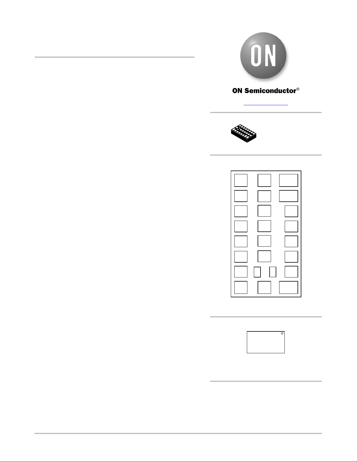
SIP25
HYBRID
CASE 127DZ
PAD CONNECTION
VIN2
D_VC
SDA
CLK
MS1
See detailed ordering and shipping information on page 13 of
this data sheet.
17
16
TIN
DAI
15
VC
14
13
12
11
MARKING DIAGRAM
SA3229 = Specific Device Code
E1 = RoHS Compliant Hybrid
XXXXXX = Work Order Number
ORDERING INFORMATION
18
VIN1
19
TR4
20
TR3
21
TR2
22
TR1
23
N/C
25 24
N/C
MS2
(Bottom View)
SA3229−E1
XXXXXX
N/C
1
VREG
2
MGND
GND
3
PGND
4
OUT+
5
OUT−
6
VBP
7
VB
8910
© Semiconductor Components Industries, LLC, 2017
March, 2021 − Rev. 4
1 Publication Order Number:
SA3229/D
Page 2
RHYTHM SA3229
• Eight Biquadratic Filters
• 16 kHz or 8 kHz Bandwidth
• Four Fully Configurable Memories with Audible
Memory Change Indicator
• 96 dB Input Dynamic Range with Headroom Extension
• 128−bit Fingerprint Security System and Other Security
Features to Protect Against Device Cloning and
Software Piracy
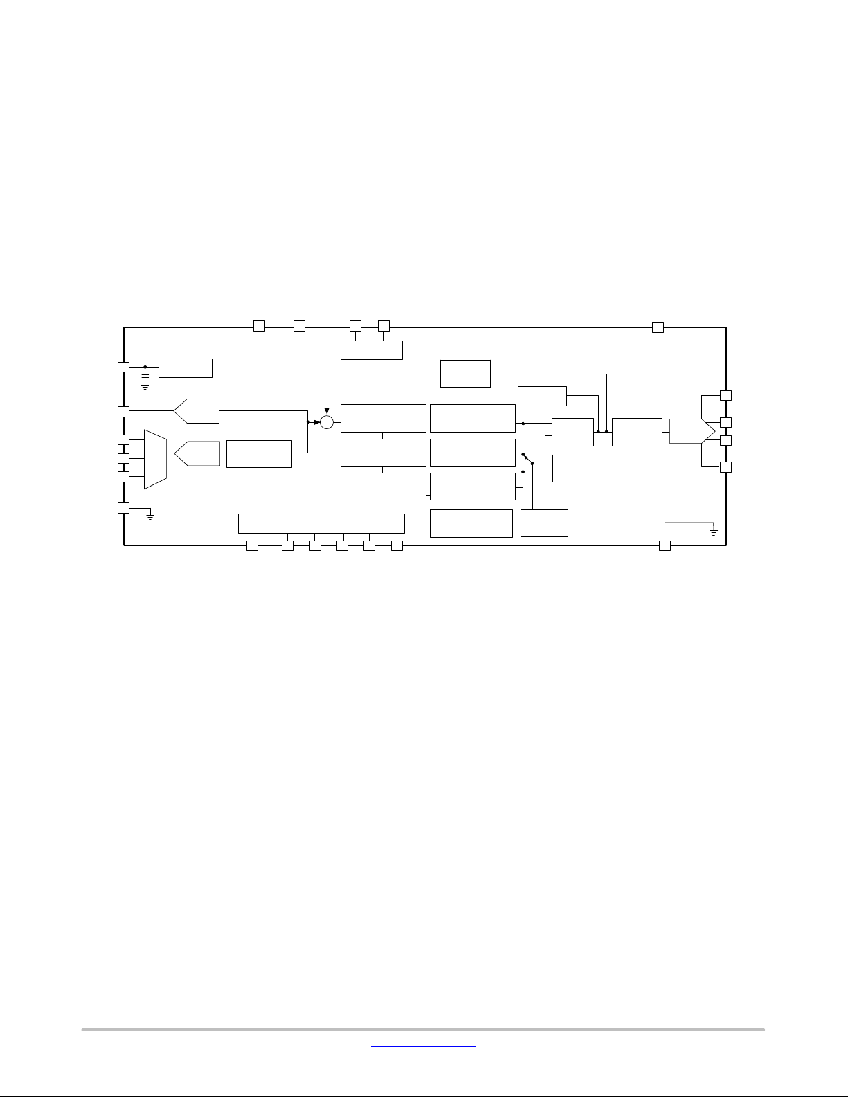
BLOCK DIAGRAM
MS2
VREG
MIC1
MIC2
TIN
DAI
MGND
1
18
17
16
15
2
SA3229
REGULATOR
A/D
A/D
910
MIC / TELECOIL
COMPENSATION
13
D_VC
MS1
TRIMMER/VC INTERFACE
14
VC
SDA CLK
12 11
PROGRAMMING
INTERFACE
PRE BIQUAD FILTERS
+
22 20 19
1−4
1, 2 or 4 CHANNEL
WDRC
POST BIQUAD FILTERS
1 & 2
21
TR4TR3TR2TR1
• High Fidelity Audio CODEC
• Soft Acoustic Fade between Memory Changes
• Drives Zero−Bias Two−Terminal Receivers
• E1 RoHS−compliant Hybrid
• Hybrid Typical Dimensions:
0.225 x 0.125 x 0.045 in
(5.72 x 3.18 x 1.14 mm)
• These Devices are Pb−Free and are RoHS Compliant
VB
8
FEEDBACK
CANCELLER
POST BIQUAD FILTERS
3 & 4
AGC−O
VC GAIN
WIDEBAND GAIN
NOISE GENERATOR
TONE
GENERATOR
BIQUAD 1−4
CROSS
FADER
EVOKE
PEAK
CLIPPING
3
GND
D/A
HBRIDGE
7
5
6
4
VBP
OUT+
OUT −
PGND
Figure 1. Hybrid Block Diagram
www.onsemi.com
2
Page 3

RHYTHM SA3229
SPECIFICATIONS
Table 1. ABSOLUTE MAXIMUM RATINGS
Parameter Value Units
Operating Temperature Range 0 to +40 °C
Storage Temperature Range −20 to +70 °C
Absolute Maximum Power Dissipation 25 mW
Maximum Operating Supply Voltage 1.65 VDC
Absolute Maximum Supply Voltage 1.8 VDC
Stresses exceeding those listed in the Maximum Ratings table may damage the device. If any of these limits are exceeded, device functionality
should not be assumed, damage may occur and reliability may be affected.
WARNING: Electrostatic Sensitive Device − Do not open packages or handle except at a static−free workstation.
WARNING: Moisture Sensitive Device − RoHS Compliant; Level 3 MSL. Do not open packages except under controlled conditions.
Table 2. ELECTRICAL CHARACTERISTICS (Supply Voltage V
Parameter
Hybrid Current I
Symbol Conditions Min Typ Max Units
AMP
All functions, 32 kHz sampling rate − 640 − mA
= 1.25 V; Temperature = 25°C)
B
All functions, 16 kHz sampling rate − 535 −
Minimum Operating Supply Voltage V
BOFF
Ramp down, audio path 0.93 0.95 0.97
Ramp down, control logic 0.77 0.80 0.83
Supply Voltage Turn On Threshold V
BON
Ramp up 1.06 1.10 1.16 V
Low Frequency System Limit − − − 125 − Hz
High Frequency System Limit − − − 16 − kHz
Total Harmonic Distortion THD VIN = −40 dBV − − 1 %
THD at Maximum Input THD
Clock Frequency f
CLK
Audio Path Latency
− 8 kHz bandwidth − 4.2 −
VIN = −15 dBV, Headroom Extension
M
− ON
− 3.973 4.096 4.218 MHz
− − 3 %
ms
− 16 kHz bandwidth − 4.0 −
System Power On Time (Note 1) − SA3229 − 700 − ms
REGULATOR
Regulator Voltage
V
REG
System PSRR PSRR
SYS
1 kHz, Input referred, Headroom
Extension enabled
− 0.87 0.90 0.93 V
− 70 − dB
INPUT
Input Referred Noise
IRN Bandwidth 100 Hz − 8 kHz,
− −108 −106 dBV
Headroom Extension on
Input Impedance Z
IN
Anti−aliasing Filter Rejection − f = f
CLK/2
1 kHz − 3 −
MW
− 8 kHz, VIN = −40 dBV − 80 − dB
Crosstalk − Between both A/D and Mux − 60 − dB
Maximum Input Level − − −15 −13 − dBV
Analogue Input Voltage Range
V
AN_IN
V
AN_TIN
V
, V
, Al 0 − 800
IN1
IN2
T
IN
Input Dynamic Range − Headroom Extension − ON
−100 − 800
− 95 96 dB
mV
Bandwidth
100 Hz − 8 kHz
V
www.onsemi.com
3
Page 4
RHYTHM SA3229
Table 2. ELECTRICAL CHARACTERISTICS (Supply Voltage V
= 1.25 V; Temperature = 25°C) (continued)
B
Parameter UnitsMaxTypMinConditionsSymbol
OUTPUT
D/A Dynamic Range
Output Impedance Z
− 100 Hz − 8 kHz − 88 − dB
OUT
− − 10 13
W
CONTROL A/D
Resolution (monotonic)
− − 7 − − bits
Zero Scale Level − − − 0 − V
Full Scale Level − − − V
REG
− V
VOLUME CONTROL
Volume Control Resistance
R
VC
Three−terminal connection 100 − 360
kW
Volume Control Range − − − − 42 dB
PC_SDA INPUT
Logic 0 Voltage
− − 0 − 0.3 V
Logic 1 Voltage − − 1 − 1.25 V
PC_SDA OUTPUT
Stand−by Pull Up Current
Sync Pull Up Current − Creftrim = 6 748 880 1020
Max Sync Pull Up Current − Creftrim = 15 − 1380 −
Min Sync Pull Up Current − Creftrim = 0 − 550 −
Logic 0 Current (Pull Down) − Creftrim = 6 374 440 506
Logic 1 Current (Pull Up) − Creftrim = 6 374 440 506
Synchronization Time
(Synchronization Pulse Width)
− Creftrim = 6 3 5 6.5
T
SYNC
Baud = 0 237 250 263 ms
Baud = 1 118 125 132
mA
mA
mA
mA
mA
mA
Baud = 2 59 62.5 66
Baud = 3 29.76 31.25 32.81
Baud = 4 14.88 15.63 16.41
Baud = 5 7.44 7.81 8.20
Baud = 6 3.72 3.91 4.10
Baud = 7 1.86 1.95 2.05
Product parametric performance is indicated in the Electrical Characteristics for the listed test conditions, unless otherwise noted. Product
performance may not be indicated by the Electrical Characteristics if operated under different conditions.
1. Times do not include additional programmable startup delay.
www.onsemi.com
4
Page 5

RHYTHM SA3229
Table 3. I2C TIMING
Standard Mode Fast Mode
Parameter Symbol
Clock Frequency f
Hold time (repeated) START condition. After this
period, the first clock pulse is generated.
LOW Period of the PC_CLK Clock t
HIGH Period of the PC_CLK Clock t
Set−up time for a repeated START condition t
Data Hold Time:
for CBUS Compatible Masters
PC_CLK
t
HD;STA
LOW
HIGH
SU;STA
t
HD;DAT
for I2C−bus Devices
Data set−up time t
Rise time of both PC_SDA and PC_CLK signals t
Fall time of both PC_SDA and PC_CLK signals t
Set−up time for STOP condition t
Bus free time between a STOP and START condition t
Output fall time from V
capacitance from 10 pF to 400 pF
IHmin
to V
ILmax
with a bus
Pulse width of spikes which must be suppressed by
the input filter
Capacitive load for each bus line C
SU;DAT
r
f
SU;STO
BUF
t
of
t
SP
b
1. A device must internally provide a hold time of at least 300 ns for the PC_SDA signal to bridge the undefined region of the falling edge of PC_CLK.
2. The maximum t
3. A Fast−mode I
has only to be met if the device does not stretch the LOW period (t
HD;DAT
2
C−bus device can be used in a Standard−mode I2C−bus system, but the requirement t
This will automatically be the case if the device does not stretch the LOW period of the PC_CLK signal. If such a device does stretch the
LOW period of the PC_CLK signal, it must output the next data bit to the PC_SDA line t
to the Standard−mode I
= total capacitance of one bus line in pF.
4. C
b
2
C−bus specification) before the PC_CLK line is released.
Min Max Min Max
0 100 0 400 kHz
4.0 − 0.6 −
4.7 − − −
4.0 − − −
4.7 − − −
5.0
0
(Note 1)
−
3.4
(Note 2)
−
0
(Note 1)
−
0.9
(Note 2)
250 − 100 − nsec
− 1000 20 + 0.1 C
(Note 4)
− 300 20 + 0.1 C
(Note 4)
b
b
300 nsec
300 nsec
4.0 − 0.6 − nsec
4.7 − 1.3 −
− 250 20 + 0.1 C
(Note 4)
b
250 nsec
n/a n/a 0 50 nsec
− 400 − 400 pF
) of the PC_CLK signal.
LOW
max + t
r
SU;DAT
P250ns must then be met.
SU;DAT
= 1000 + 250 = 1250 ns (according
Units
msec
msec
msec
msec
msec
msec
www.onsemi.com
5
Page 6

RHYTHM SA3229
TYPICAL APPLICATIONS
V
B
910
REGULATOR
1
3k9
18
17
16
1k
15
2
SA3229
A/D
A/D
MIC / TELECOIL
COMPENSATION
TRIMMER/VC INTERFACE
13
14
12 11 8
PROGRAMMING
INTERFACE
PRE BIQUAD FILTERS
+
22 20 19
1−4
1, 2 or 4 CHANNEL
WDRC
POST BIQUAD FILTERS
1 & 2
21
FEEDBACK
CANCELLER
POST BIQUAD FILTERS
AGC−O
VC GAIN
WIDEBAND GAIN
NOISE GENERATOR
Note: All resistors in ohms and all capacitors in farads, unless otherwise stated.
Figure 2. Test Circuit
Reed Switch
For Autotcoil
12 11 8
PROGRAMMING
INTERFACE
PRE BIQUAD FILTERS
+
22 20 19
1−4
1, 2 or 4 CHANNEL
WDRC
POST BIQUAD FILTERS
1 & 2
21
POST BIQUAD FILTERS
NOISE GENERATOR
1
18
17
16
15
2
SA3229
REGULATOR
A/D
A/D
910
MIC / TELECOIL
COMPENSATION
13
TRIMMER/VC INTERFACE
14
3 & 4
MS
FEEDBACK
CANCELLER
3 & 4
AGC−O
VC GAIN
WIDEBAND GAIN
TONE
GENERATOR
BIQUAD 1−4
GENERATOR
BIQUAD 1−4
CROSS
FADER
EVOKE
TONE
CROSS
FADER
EVOKE
PEAK
CLIPPING
D/A
HBRIDGE
3
PEAK
CLIPPING
D/A
HBRIDGE
3
7
LP FILTER
V
OUT
B
5
6
4
22
47μ
7
5
6
4
VC
TR1 TR2 TR3
TR4
Note: All resistors in ohms and all capacitors in farads, unless otherwise stated.
Figure 3. Typical Trimmer Application Circuit
www.onsemi.com
6
Page 7

RHYTHM SA3229
SA3229 OVERVIEW
SA3229 is a DSP system implemented on
ON Semiconductor’s Wolverine hardware platform.
Wolverine is the hearing industry’s first 90 nm
Silicon−on−Chip platform enabling design of
highly−efficient and flexible hearing aid solutions. The
device is packaged for easy integration into a wide range of
applications from CIC to BTE. SA3229 can be used as a
trimmer adjustable device. It may be configured as one, two
or four channels with linear or WDRC processing.
Configuration data stored in non−volatile memory defines
hearing−aid parameters. SA3229 can be programmed via
the SDA or I
The DSP core implements Adaptive Feedback
Cancellation, compression, wideband gain, and volume
control. The Adaptive Feedback Canceller reduces acoustic
feedback while offering robust performance against pure
tones.
SA3229 is an economical variant of SB3229 which
utilizes the on−chip non−volatile memory on Wolverine
(OTP) to offer the extended Rhythm feature set in a low−cost
solution. Device settings are programmed into the OTP
A/D and D/A Converter
The system’s A/D converter is a 2nd−order sigma−delta
modulator operating at a 2.048 MHz sample rate.
The system’s input is pre−conditioned with anti−alias
filtering and a programmable gain pre−amplifier. The
analog output is oversampled and modulated to produce a
1−bit pulse density modulated (PDM) data stream. The
digital PDM data is then decimated down to pulse−code
modulated (PCM) digital words at the system’s sampling
rate of 32 kHz.
The D/A is comprised of a digital 3rd−order sigma−delta
modulator and an H−bridge. The modulator accepts PCM
audio data from the DSP path and converts it into a 64−times
oversampled, 1−bit PDM data stream, which is then
supplied to the H−bridge. The H−bridge is a specialized
CMOS output driver used to convert the 1−bit data stream
into a low−impedance, differential output voltage
waveform suitable for driving zero−biased hearing aid
receivers.
Analog Inputs
SA3229 provides for up to four analog inputs,
Microphone 1 (MIC1), Microphone 2 (MIC2), Telecoil
(TCOIL) and Direct Audio Input (DAI) with the following
configurable front end modes:
2
C programming interfaces.
FUNCTIONAL BLOCK DESCRIPTION
memory during manufacturing and fitting adjustments can
be made with up to four trimmers.
SA3229 and SB3229 feature identical parameter sets.
Therefore, SB3229 can be used for design and development
purposes. At manufacturing time, customers have the option
to migrate to the cost−efficient SA3229 variant, enabling
low−cost Bill−of−Materials for cost sensitive applications.
SA3229 supports two times programming, which provides
flexibility to rework the product, should any design changes
be needed.
Development of SA3229 based products is identical to the
SB3229 products using identical ARK libraries. The
SA3229 hybrid, however, can only be programmed in a
manufacturing environment using Cal/Config.
During trimmer mode operation, a low−speed A/D circuit
monitors the positions of up to four manual trimmers and
a VC potentiometer. Trimmer position changes are
immediately interpreted and translated into new circuit
parameter values, which are then used to update the signal
path.
• MIC1
• MIC2
• DAI
• TCOIL
• MIC1 + TCOIL
• MIC1 + DAI
Attenuation can be applied to the MIC1 input when
mixing with either TCOIL or DAI inputs.
Analog input signals should be ground referenced to
MGND. (Microphones, telecoils, DAI). MGND is
internally connected to GND to minimize noise, and should
not be connected to any external ground point.
Channel Processing
Figure 4 represents the I/O characteristic of independent
AGC channel processing. The I/O curve can be divided into
four main regions:
• Low input level expansion (squelch) region
• Low input level linear region
• Compression region
• High input level linear region (return to linear)
www.onsemi.com
7
Page 8

RHYTHM SA3229
0
−10
−20
−30
Low Level
Gain
−40
−50
−60
−70
OUTPUT LEVEL (dBV)
−80
−90
−100
−120 −110 −100 −90 −80 −70 −60 −50 −40 −30 −20
Figure 4. Independent Channel I/O Curve Flexibility
Compression
Ratio
Lower
Threshold
Squelch
Threshold
INPUT LEVEL (dBV)
High Level
Gain
Upper
Threshold
Channel I/O processing is specified by the Squelch
threshold (SQUELCHTH) and any four of the following
five parameters (only four of the five properties are
independent):
• Low level gain (LLGAIN)
• Lower threshold (LTH)
• High level gain (HLGAIN)
• Upper threshold (UTH)
• Compression ratio (CR)
During the Parameter Map creation, constraints are
applied to the compression parameters to ensure that the I/O
characteristics are continuous. Parameter adjustments
support two popular styles of compression ratio adjustment:
• The compression region of the I/O curve pivots about
the upper threshold. As the compression ratio trimmer
is adjusted, high−level gain remains constant while
the low−level gain changes.
• The compression region of the I/O curve pivots about
the lower threshold. Low−level gain remains constant
as the compression ratio trimmer is adjusted.
The squelch region within each channel implements a low
level noise reduction scheme (1:3 expansion) for listener
comfort. This scheme operates in quiet listening
environments (programmable threshold) to reduce the gain
at very low levels.
Automatic Telecoil
The automatic telecoil feature in SA3229 is to be used
with memory D programmed with the telecoil or
MIC + TCOIL front end configuration. The feature enables
the part to transition to memory D upon the closing of
a switch connected to MS2. With the feature enabled and
a reed switch connected to MS2, the static magnetic field of
a telephone handset will close the switch whenever the
handset is brought close to the device, causing the hybrid to
change to memory D. The part will transition back to the
initial memory once the switch is deemed opened after
proper debouncing.
A debounce algorithm with a programmable debounce
period is used to prevent needless switching in and out of
memory D due to physical switch bounces when MS2 is
configured for automatic telecoil. Upon detecting a close to
open switch transition, the debounce algorithm monitors the
switch status. The debounce algorithm switches the device
out of memory D only once the switch signal has been
continuously sampled open over the specified debounce
period.
Adaptive Feedback Canceller
The Adaptive Feedback Canceller (AFC) reduces
acoustic feedback by forming an estimate of the hearing aid
feedback signal and then subtracting this estimate from the
hearing aid input. The forward path of the hearing aid is not
affected. Unlike adaptive notch filter approaches, SM3229’s
AFC does not reduce the hearing aid’s gain. The AFC is
based on a time−domain model of the feedback path.
The third−generation AFC (see Figure 5) allows for an
increase in the stable gain
1
of the hearing instrument while
minimizing artefacts for music and tonal input signals. As
with previous products, the feedback canceller provides
completely automatic operation.
1. Added stable gain will vary based on hearing aid style and
acoustic setup. Please refer to the Adaptive Feedback
Cancellation Information note for more details
Feedback path
+
Σ
−
Estimated feedback
Figure 5. Adaptive Feedback Canceller (AFC)
Block Diagram
H
G
H’
Volume Control, Trimmers and Switches
External Volume Control
The volume of the device can either be set statically via
software or controlled externally via a physical interface.
SA3229 supports both analog and digital volume control
functionality, although only one can be enabled at a time.
Digital control is supported with either a momentary switch
or a rocker switch. In the latter case, the rocker switch can
also be used to control memory selects.
Analog Volume Control
Both the external (analog) volume control and trimmers
work with a three−terminal 100 kW – 360 kW variable
resistor. The volume control can have either a log or linear
www.onsemi.com
8
Page 9

RHYTHM SA3229
taper, which is selectable via software. It is possible to use
a VC with up to 1 MW of resistance, but this could result in
a slight decrease in the resolution of the taper.
Trimmers
The trimmer interface provides the ability to control up to
19 hearing aid parameters through up to four trimmers.
A single trimmer parameter can have up to 16 values and
a single trimmer can control multiple parameters
(e.g., Trimmer 1 can control compression ratio in all four
channels simultaneously). The trimmer must be
three−terminal 100 kW to 360 kW variable resistors and have
a linear taper.
Parameters that can be assigned to trimmers include Low
Cut, High Cut, Compression Ratio, Wideband Gain,
Tinnitus Noise Level, Crossover Frequency, Lower
Threshold, Upper Threshold, EQ Gain, Squelch Threshold,
High Level Gain, Low Level Gain, AGC−O Threshold,
Static Volume Control and Peak Clipper Threshold.
Digital Volume Control
The digital volume control makes use of two pins for
volume control adjustment, VC and D_VC, with
momentary switches connected to each. Closure of the
switch to the VC pin indicates a gain increase while closure
to the D_VC pin indicates a gain decrease. Figure 6 shows
how to wire the digital volume control to SA3229.
GND
VC
D_VC
Figure 6. Wiring for Digital Volume Control
Memory Select Switches
One or two, two−pole Memory Select (MS) switches can
be used with SA3229. This enables user’s tremendous
flexibility in switching between configurations. Up to four
memories can be configured and selected by the MS
switches on SA3229. Memory A must always be valid. The
MS switches are either momentary or static and are fully
configurable through IDS in the IDS setting tab.
The behavior of the MS switches is controlled by two main
parameters in IDS:
MSSmode: this mode determines whether
a connected switch is momentary or static.
Donly: this parameter determines whether the MS2
switch is dedicated to the last memory position.
There are four basic MS switch modes of operation as shown
in Table 4 below.
Table 4. MS SWITCH MODES
Max # of Valid
MS Switch Mode MS1 Switch MS2 Switch
Mode 1 Momentary None 4 Off Momentary Simplest configuration
Mode 2 Momentary Static 4 On Momentary Jump to last memory
Mode 3 Static Static 4 Off Static Binary selection of memory
Mode 4 Static Static 3 On Static Jump to last memory
The flexibility of the MS switches is further increased by
allowing the MS switches to be wired to GND or VBAT,
corresponding to an active low or active high logic level on
Table 5. MS SWITCH LOGIC LEVELS VS. IDS PULLUPDOWN SETTINGS
“PullUpDown” Setting in IDS MS Switch State MS Input Logic Level Switch Connection
Pulldown CLOSED HI To VBAT
Pulldown OPEN LOW To VBAT
Pullup CLOSED LOW To GND
Pullup OPEN HI To GND
Memories
Donly MSSMode Use
the MS pins. This option is configured with the
MSPullUpDown/MS2PullUpDown setting in the IDS
settings tab as shown in Table 5 below.
www.onsemi.com
9
Page 10

RHYTHM SA3229
In the following mode descriptions, it is assumed that the
PullUpDown setting has been properly configured for the
MS switch wiring so that a CLOSED switch state is at the
correct input logic level.
Mode 1: Momentary Switch on MS1
This mode uses a single momentary switch on MS1 input
to change memories. Using this mode causes the part to start
in memory A, and whenever the button is pressed, the next
valid memory is loaded. When the user is in the last valid
memory, a button press causes memory A to be loaded.
Thus, the possible selection sequences are:
If 4 valid memories: ABCDABCDA…
If 3 valid memories: ABCABCA…
If 2 valid memories: ABABA…
If 1 valid memory: AAA…
Mode 2: Momentary Switch on MS1, Static Switch on
MS2
(D−only, Jump to Last Memory)
This mode uses a static switch on MS2 and a momentary
switch on MS1 to change memories. It can be used to support
the Automatic Telecoil feature, see section Automatic
Telecoil.
If the static switch on MS2 is OPEN, the part starts in
memory A and is controlled by the momentary switch on
MS1 as described in section Momentary Switch on MS1,
with the exception that memory D is not used. If the static
switch on MS2 is set to CLOSED, the part automatically
jumps to memory D (occurs on startup or during normal
operation). In this setup, the state of the momentary switch
on MS1 is ignored. When MS2 is set to OPEN, the part loads
in the memory that was active prior to jumping to memory
D.
The possible memory selection sequences are:
If MS2 = OPEN and there are four valid memories, MS1
selects: ABCABCA…
If MS2 = OPEN and there are three valid memories, MS1
selects: ABABA…
If MS2 = OPEN and there is one valid memory: A
If MS2 = CLOSED: D
Mode 3: Static Switch on MS1 and MS2
This mode uses two static switches to change memories.
In this mode, it is possible to jump from any memory to any
other memory by changing the state of both switches. If the
two switches are changed one after the other, the part
transitions to an intermediate memory before reaching the
final memory. The part starts in whatever memory the
switches are selecting. If a memory is invalid, the part
defaults to memory A.
Table 6. STATIC SWITCH TRUTH TABLE:
D−ONLY DISABLED
Binary State (MS1/MS2) Selected Memory
OPEN OPEN Memory A
CLOSED OPEN Memory B
OPEN CLOSED Memory C
CLOSED CLOSED Memory D
Mode 4: Static Switch on MS1, Static Switch on MS2
(D−only, Jump to Last Memory)
This mode uses two static switches to change memories.
Similar to the behaviour described in the Static Switch on
MS1 and MS2 section, this mode will switch to memory D
if the static switch on MS2 is CLOSED (the state of the
switch on MS1 is ignored). The mode, however, supports a
maximum of three memories (even if four valid memories
are programmed). This mode can be used to support the
Automatic Telecoil feature (see the Automatic Telecoil
section).
In this mode, it is possible to jump from any memory to
any other memory by changing the state of both switches. If
the two switches are changed one after the other, the part
transitions to an intermediate memory before reaching the
final memory.
The part starts in whatever memory the switches are
selecting. If a memory is invalid, the part defaults to
memory A.
Table 7. STATIC SWITCH TRUTH TABLE:
D−ONLY ENABLED; (EXAMPLE WITH THREE VALID
MEMORIES)
Binary State (MS1/MS2) Selected Memory
OPEN OPEN Memory A
CLOSED OPEN Memory B
X CLOSED Memory D
Rocker Switch Support
The device supports connection of a rocker switch to the
digital volume control interface that can perform volume
control (VC) adjustments and/or memory selection (MS).
There are three modes of operation:
• Digital Volume Control Mode
• Momentary Memory Select Mode
• Mixed Mode (VC and MS)
In Digital VC mode, the rocker switch provides the digital
volume control functionality as described in this section.
www.onsemi.com
10
Page 11

RHYTHM SA3229
In Momentary Memory Select mode, the rocker switch
allows cycling through the memory profiles in both
directions. An “up” switch closure indicates a program
advance to the next higher numbered memory and “down”
switch closures indicates a program retreat to the next lower
numbered memory. In this mode, volume control is only
available through software control.
In Mixed Mode, operation of the switch as a volume
control or memory select is governed by the time duration
of the switch closure: either short or long. The
discrimination of short and long pulses is set by
a programmable, time−threshold value, from 1 s to 5 s in 1 s
increments. An additional programmable parameter
determines whether the short pulses refer to volume−control
operation or memory−select operation.
If long pulses control memory select operation, the
memory change is initiated once the switch is held for the
long pulse period without requiring the switch to be
released. In Digital VC mode or Momentary Memory Select
mode, the action takes place after the switch is released.
AGC−O
The AGC−O module is an output limiting circuit with
a fixed compression ratio of ∞ : 1. The limiting level is
programmable as a level measured in dB from full scale. The
maximum output of the device is 0 dBFS.
The AGC−O module has its own level detector, with
programmable attack and release time constants.
Graphic Equalizer
SA3229 has a 8−band graphic equalizer. Each band
provides up to 24 dB of gain adjustment in 1 dB increments.
Biquadratic Filters
Additional frequency shaping can be achieved by
configuring generic biquad filters. The transfer function for
each of the biquad filters is as follows:
H(z) +
*1
b0 ) b1 z
) b2 z
1 ) a1 z*1) a2 z
*2
*2
NOTE: The a0 coefficient is hard−wired to always be
‘1’. The coefficients are each 16 bits in length
and formatted as one sign bit, one integer bit and
14 fractional bits. This maps onto a decimal
range of −2.0 to 2.0 before quantization (−32767
to 32767 after quantization).
Thus, before quantization, the floating−point coefficients
must be in the range −2.0 ≤ x < 2.0 and quantized with the
function:
round(x 2
14
)
After designing a filter, the quantized coefficients can be
entered into the PreBiquads or PostBiquads tab in the
Interactive Data Sheet. The coefficients b0, b1, b2, a1, and
a2 are as defined in the transfer function above. The
parameters meta0 and meta1 do not have any effect on the
signal processing, but can be used to store additional
information related to the associated biquad.
The underlying code in the product components
automatically checks all of the filters in the system for
stability (i.e., the poles have to be within the unit circle)
before updating the graphs on the screen or programming
the coefficients into the hybrid. If the Interactive Data Sheet
receives an exception from the underlying stability checking
code, it automatically disables the biquad being modified
and displays a warning message. When the filter is made
stable again, it can be re−enabled.
Also note that in some configurations, some of these
filters may be used by the product component for
microphone/telecoil compensation, low−frequency EQ, etc.
If this is the case, the coefficients entered by the user into
IDS are ignored and the filter designed by the software is
programmed instead. For more information on filter design
refer to the Biquad Filters In PARAGON Digital Hybrid
information note.
Tinnitus Treatment Noise
The Tinnitus Treatment noise is generated using white
noise generator hardware and shaping the generated noise
using four 2
nd
order biquadratic filters. The filter parameters
are the same coefficients as those presented in the
Biquadratic Filters section.
The Tinnitus Treatment noise can be added into the signal
path at two possible locations: before the VC (before the
AGC−O, but compensated for the Wideband Gain) or after
the VC (between the last generic biquad and the Cross
Fader).
If the noise is injected before the VC then the level of the
noise will change along with the rest of the audio through the
device when the VC is adjusted. If the noise is injected after
the VC it is not affected by VC changes.
EVOKE Acoustic Indicators
Ten Acoustic Indicators are available for indicating
events. Each indicator is fixed to a particular event. Any
event can have its assigned indicator enabled or disabled
although not always independently. Individual enable/
disable control is provided for the following event or group
of events:
• Power on reset (POR)
• Four memory selects
• Volume Up and Volume Down
• Volume Max and Volume Min
• Low Battery
Each Acoustic Indicator is made up of up to four faded
tones. A faded tone exhibits a 64 ms fade−in and fade−out
transition time. The duration of an Acoustic Indicator is
configurable, with a maximum value of 6.35 seconds.
Power Management
SA3229 has three user−selectable power management
schemes to ensure the hearing aid dies gracefully at the end
of battery life. Shallow reset, Deep reset and Advanced
www.onsemi.com
11
Page 12

RHYTHM SA3229
Reset mode. It also contains a programmable power on reset
delay function.
Power On Reset Delay
The programmable POR delay controls the amount of
time between power being connected to the hybrid and the
audio output being enabled. This gives the user time to
properly insert the hearing aid before the audio starts,
avoiding the temporary feedback that can occur while the
device is being inserted. During the delay period,
momentary button presses are ignored.
Power Management Functionality
As the voltage on the hearing aid battery decreases, an
audible warning is given to the user indicating the battery
life is low. In addition to this audible warning, the hearing
aid takes other steps to ensure proper operation given the
weak supply. The exact hearing aid behaviour in low supply
conditions depends on the selected POR mode. The hearing
aid has three POR modes:
• Shallow Reset Mode
• Deep Reset Mode
• Advanced Mode
Shallow Reset Mode
In Shallow Reset mode, the hearing aid will operate
normally when the battery is above 0.95 V. Once the supply
voltage drops below 0.95 V the audio will be muted and
remain in that state until the supply voltage rises above
1.1 V. Once the supply voltage drops below the control logic
ramp down voltage, the device will undergo a hardware
reset. At this point, the device will remain off until the supply
voltage returns to 1.1 V. When the supply voltage is below
the control logic voltage, but above 0.6 V and rises above the
1.1 V turn on threshold, the device will activate its output
and operate from the memory that was active prior to reset.
If the supply voltage drops below 0.6 V, and rises above the
1.1 V turn on threshold, the device will reinitialize, activate
its output and operate from memory A.
Deep Reset Mode
In Deep Reset mode, the hearing aid will operate normally
when the battery is above 0.95 V. Once the supply voltage
drops below 0.95 V the audio will be muted. The device
remains in this state until the supply voltage drops below the
hardware reset voltage of 0.6 V. When this occurs, the
device will load memory A and operate normally after the
supply voltage goes above 1.1 V.
Advanced Reset Mode
Advanced Reset Mode on SA3229 is a more sophisticated
power management scheme than shallow and deep reset
modes. This mode attempts to maximize the device’s usable
battery life by reducing the gain to stabilize the supply based
on the instantaneous and average supply voltage levels.
Instantaneous supply fluctuations below 0.95 V can trigger
up to two 3 dB, instantaneous gain reductions. Average
supply drops below 0.95 V can trigger up to eighteen, 1 dB
average gain reductions.
While the average supply voltage is above 0.95 V, an
instantaneous supply voltage fluctuation below 0.95 V will
trigger an immediate 3 dB gain reduction. After the 3 dB
gain reduction has been applied, the advanced reset model
holds off checking the instantaneous voltage level for
a monitoring period of 30 second in order to allow the
voltage level to stabilize. If after the stabilization time the
instantaneous voltage drops a second time below 0.95 V
during the next monitoring period, the gain will be reduced
an additional 3 dB for a 6 dB total reduction and a 30 second
stabilization time is activated. The advanced reset mode
continues to monitor the instantaneous voltage levels over
30 second monitoring periods. If the instantaneous voltage
remains above 1.1 V during that monitoring period, the gain
will be restored to the original setting regardless of whether
one or two gain reductions are applied. If two gain
reductions are applied and the instantaneous voltage level
remains above 1.0 V for a monitoring period, the gain will
be restored to a 3 dB reduction.
Should the average supply voltage drop below 0.95 V, the
device will then reduce the gain by 1 dB every 10 seconds
until either the average supply voltage rises above 0.95 V or
a total of 18 average gain reductions have been applied, at
which point the audio path will be muted. If the average
supply voltage returns to a level above 1.1 V, the audio path
will first be un−muted, if required. The gain will then be
increased by 1 dB every 10 seconds until either the average
supply voltage drops below 1.1 V, or all average gain
reductions have been removed. No action is taken while the
average supply voltage resides between 0.95 V and 1.1 V.
NOTE: Instantaneous and average gain reductions are
adjusted independently.
When the instantaneous voltage falls below the hardware
shutdown voltage, the device will undergo a hardware reset.
When it turns back on because the voltage has risen above
the turn−on threshold of 0.6 V, it will behave the same as it
would in shallow reset mode.
Low Battery Notification
Notification of the low battery condition via an acoustic
indicator is optionally performed when the battery voltage
drops below a configurable low battery notification
threshold. The low battery indicator is repeated every five
minutes until the device shuts down.
SDA and I2C Communication
The SA3229 OTP can be programmed using the SDA or
2
I
C protocol. During parameter changes, the main audio
signal path of the hybrid is temporarily muted using the
memory switch fader to avoid the generation of disturbing
audio transients. Once the changes are complete, the main
audio path is reactivated.
Improvements have been made to the ARK software,
resulting in improved communication speed. Certain
parameters in ARKonline can be selected to reduce the
number of pages that need to be read out. In SDA mode,
SA3229 is programmed via the SDA pin using industry
www.onsemi.com
12
Page 13

RHYTHM SA3229
standard programming boxes. I2C mode is a two−wire
interface which uses the SDA pin for bidirectional data and
CLK as the interface clock input. I
2
C programming support
is available on the HiPro (serial or USB versions) and
ON Semiconductor’s DSP Programmer 3.0.
Input Connection and Layout Considerations
It is recommended to connect unused audio input pins
directly to MGND to minimize the possibility of noise
pickup. Inputs are internally AC coupled, so there is no
additional leakage current when inputs are connected
• MGND is used as reference ground plane for input
signals. All input components should be grounded to
MGND. This ground plane should be isolated from all
other ground connections in the system.
• Keep the input traces as short as possible and avoid
routing traces near high noise sources such as the
OUT+ and OUT− pins
• Star ground input component grounds to the MGND
connection.
Unused trimmer inputs should also be connected to GND.
directly to ground.
In order to further minimize noise at the inputs the following
guidelines are recommended:
ORDERING INFORMATION
Device Package Shipping
SA3229−E1 25 Pad Hybrid
Case 127DZ
SA3229−E1−T 25 Pad Hybrid
Case 127DZ
†For information on tape and reel specifications, including part orientation and tape sizes, please refer to our Tape and Reel Packaging
Specifications Brochure, BRD8011/D.
Hybrid Jig Ordering Information
25 Units / Bubble Pack
250 Units / Tape & Reel
†
To order a Hybrid Jig Evaluation Board for SA3229 contact your Sales Account Manager or FAE and use part number
SA3404GEVB.
www.onsemi.com
13
Page 14

RHYTHM SA3229
PAD LOCATIONS
Table 8. PAD POSITION AND DIMENSIONS
mil mm
Pad No Pin Name X Y Xdim Ydim X Y Xdim Ydim
1 VREG −94.5 40.0 20.0 33.0 −2.4003 1.0160 0.5080 0.8382
2 MGND −67.5 40.0 20.0 23.0 −1.7145 1.0160 0.5080 0.5842
3 GND −40.5 45.0 20.0 33.0 −1.0287 1.1430 0.5080 0.8382
4 PGND −13.5 45.0 20.0 23.0 −0.3429 1.1430 0.5080 0.5842
5 OUT+ 13.5 45.0 20.0 23.0 0.3429 1.1430 0.5080 0.5842
6 OUT− 40.5 45.0 20.0 23.0 1.0287 1.1430 0.5080 0.5842
7 VBP 67.5 45.0 20.0 23.0 1.7145 1.1430 0.5080 0.5842
8 VB 94.5 40.0 20.0 33.0 2.4003 1.0160 0.5080 0.8382
9 MS2 94.5 −2.0 20.0 23.0 2.4003 −0.0508 0.5080 0.5842
10 MS1 94.5 −45.0 20.0 23.0 2.4003 −1.1430 0.5080 0.5842
11 CLK 67.5 −45.0 20.0 23.0 1.7145 −1.1430 0.5080 0.5842
12 SDA 40.5 −45.0 20.0 23.0 1.0287 −1.1430 0.5080 0.5842
13 D_VC 13.5 −45.0 20.0 23.0 0.3429 −1.1430 0.5080 0.5842
14 VC −13.5 −45.0 20.0 23.0 −0.3429 −1.1430 0.5080 0.5842
15 DAI −40.5 −45.0 20.0 23.0 −1.0287 −1.1430 0.5080 0.5842
16 TIN −67.5 −45.0 20.0 23.0 −1.7145 −1.1430 0.5080 0.5842
17 MIC2 −94.5 −45.0 20.0 23.0 −2.4003 −1.1430 0.5080 0.5842
18 MIC1 −94.5 −2.0 20.0 23.0 −2.4003 −0.0508 0.5080 0.5842
19 TR4 −67.5 −2.0 20.0 23.0 −1.7145 −0.0508 0.5080 0.5842
20 TR3 −40.5 −2.0 20.0 23.0 −1.0287 −0.0508 0.5080 0.5842
21 TR2 −13.5 −2.0 20.0 23.0 −0.3429 −0.0508 0.5080 0.5842
22 TR1 13.5 −2.0 20.0 23.0 0.3429 −0.0508 0.5080 0.5842
23 GPIO6 40.5 −2.0 20.0 23.0 1.0287 −0.0508 0.5080 0.5842
24 DVREG 67.5 13.5 18.0 12.0 1.7145 0.3429 0.4572 0.3048
25 VPP 67.5 −13.5 18.0 12.0 1.7145 −0.3429 0.4572 0.3048
RHYTHM is a trademarks of Semiconductor Components Industries, LLC.
www.onsemi.com
14
Page 15

MECHANICAL CASE OUTLINE
PACKAGE DIMENSIONS
SCALE 2:1
SIP25, 5.72x3.18
CASE 127DZ
ISSUE A
DATE 06 DEC 2019
GENERIC
MARKING DIAGRAM*
XXXXXXXXXX
ZZZZZZ
DOCUMENT NUMBER:
DESCRIPTION:
ON Semiconductor and are trademarks of Semiconductor Components Industries, LLC dba ON Semiconductor or its subsidiaries in the United States and/or other countries.
ON Semiconductor reserves the right to make changes without further notice to any products herein. ON Semiconductor makes no warranty, representation or guarantee regarding
the suitability of its products for any particular purpose, nor does ON Semiconductor assume any liability arising out of the application or use of any product or circuit, and specifically
disclaims any and all liability, including without limitation special, consequential or incidental damages. ON Semiconductor does not convey any license under its patent rights nor the
rights of others.
© Semiconductor Components Industries, LLC, 2018
XXXX = Specific Device Code
ZZZ = Assembly Lot Code
98AON11276G
SIP25, 5.72x3.18
*This information is generic. Please refer to
device data sheet for actual part marking.
Pb−Free indicator, “G” or microdot “G”, may
or may not be present. Some products may
not follow the Generic Marking.
Electronic versions are uncontrolled except when accessed directly from the Document Repository.
Printed versions are uncontrolled except when stamped “CONTROLLED COPY” in red.
PAGE 1 OF 1
www.onsemi.com
Page 16

ON Semiconductor and are trademarks of Semiconductor Components Industries, LLC dba ON Semiconductor or its subsidiaries in the United States and/or other countries.
ON Semiconductor owns the rights to a number of patents, trademarks, copyrights, trade secrets, and other intellectual property. A listing of ON Semiconductor ’s product/patent
coverage may be accessed at www.onsemi.com/site/pdf/Patent−Marking.pdf
ON Semiconductor makes no warranty, representation or guarantee regarding the suitability of its products for any particular purpose, nor does ON Semiconductor assume any liability
arising out of the application or use of any product or circuit, and specifically disclaims any and all liability, including without limitation special, consequential or incidental damages.
Buyer is responsible for its products and applications using ON Semiconductor products, including compliance with all laws, regulations and safety requirements or standards,
regardless of any support or applications information provided by ON Semiconductor. “Typical” parameters which may be provided in ON Semiconductor data sheets and/or
specifications can and do vary in different applications and actual performance may vary over time. All operating parameters, including “Typicals” must be validated for each customer
application by customer’s technical experts. ON Semiconductor does not convey any license under its patent rights nor the rights of others. ON Semiconductor products are not
designed, intended, or authorized for use as a critical component in life support systems or any FDA Class 3 medical devices or medical devices with a same or similar classification
in a foreign jurisdiction or any devices intended for implantation in the human body. Should Buyer purchase or use ON Semiconductor products for any such unintended or unauthorized
application, Buyer shall indemnify and hold ON Semiconductor and its officers, employees, subsidiaries, affiliates, and distributors harmless against all claims, costs, damages, and
expenses, and reasonable attorney fees arising out of, directly or indirectly, any claim of personal injury or death associated with such unintended or unauthorized use, even if such
claim alleges that ON Semiconductor was negligent regarding the design or manufacture of the part. ON Semiconductor is an Equal Opportunity/Affirmative Action Employer. This
literature is subject to all applicable copyright laws and is not for resale in any manner.
. ON Semiconductor reserves the right to make changes without further notice to any products herein.
PUBLICATION ORDERING INFORMATION
LITERATURE FULFILLMENT:
Email Requests to: orderlit@onsemi.com
ON Semiconductor Website: www.onsemi.com
TECHNICAL SUPPORT
North American Technical Support:
Voice Mail: 1 800−282−9855 Toll Free USA/Canada
Phone: 011 421 33 790 2910
Europe, Middle East and Africa Technical Support:
Phone: 00421 33 790 2910
For additional information, please contact your local Sales Representative
◊
www.onsemi.com
1
 Loading...