

Page 1
查询RB751V40T1供应商
RB751V40T1
Schottky Barrier Diode
These Schottky barrier diodes are designed for high speed switching
applications, circuit protection, and voltage clamping. Extremely low
forward voltage reduces conduction loss. Miniature surface mount
package is excellent for hand held and portable applications where
space is limited.
• Extremely Fast Switching Speed
• Extremely Low Forward Voltage – 0.28 Volts (Typ) @ I
• Low Reverse Current
= 1 mAdc
F
http://onsemi.com
40 V SCHOTTKY
BARRIER DIODE
MAXIMUM RATINGS
Rating Symbol Value Unit
Peak Reverse Voltage V
Reverse Voltage V
Electrostatic Discharge E
THERMAL CHARACTERISTICS
Characteristic Symbol Max Unit
Total Device Dissipation FR–5 Board,
(Note 1.) T
Derate above 25°C
Thermal Resistance Junction to Ambient R
Junction and Storage
Temperature Range
1. FR–5 Minimum Pad
= 25°C
A
P
TJ, T
RM
SD
R
D
JA
stg
40 V
30 Vdc
HBM Class: 1C
MM Class: A
200
1.57mWmW/°C
635 °C/W
–55 to
+150
°C
1
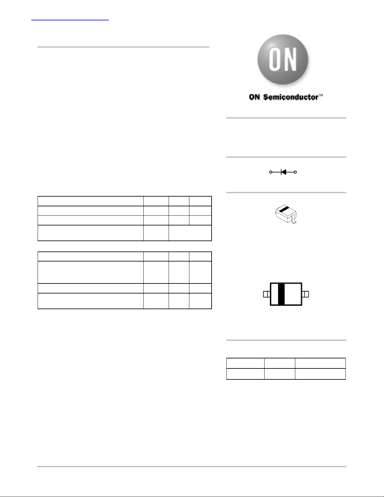
CATHODE
1
SOD–323
CASE 477
PLASTIC
2
ANODE
2
MARKING DIAGRAMS
5E M
5E = Specific Device Code
M = Date Code
ORDERING INFORMATION
Semiconductor Components Industries, LLC, 2001
May, 2001 – Rev. 1
Device Package Shipping
RB751V40T1 SOD–323 3000/Tape & Reel
1 Publication Order Number:
RB751V40T1/D
Page 2
RB751V40T1
ELECTRICAL CHARACTERISTICS (T
Characteristic Symbol Min Typ Max Unit
Reverse Breakdown Voltage
(I
= 10 µA)
R
Total Capacitance
(V
= 1.0 V, f = 1.0 MHz)
R
Reverse Leakage
(V
= 30 V)
R
Forward Voltage
= 1.0 mAdc)
(I
F
820 Ω
+10 V
50 Ω OUTPUT
PULSE
GENERATOR
0.1 µF
2 k
100 µH
I
F
DUT
= 25°C unless otherwise noted)
A
0.1 µF
50 Ω INPUT
SAMPLING
OSCILLOSCOPE
V
R
V
(BR)R
C
T
I
R
V
F
t
t
r
p
10%
90%
INPUT SIGNAL
30 – – Volts
– 2.0 2.5 pF
– 300 500 nAdc
– 0.28 0.37 Vdc
I
F
t
t
rr
I
R
i
R(REC)
t
= 1 mA
OUTPUT PULSE
(I
= IR = 10 mA; measured
F
at i
R(REC)
= 1 mA)
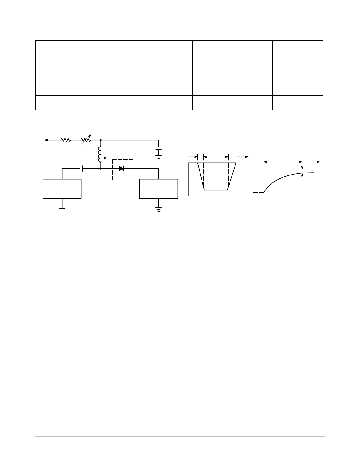
Notes: 1. A 2.0 kΩ variable resistor adjusted for a Forward Current (IF) of 10 mA.
Notes: 2. Input pulse is adjusted so I
Notes: 3. t
» t
p
rr
is equal to 10 mA.
R(peak)
Figure 1. Recovery Time Equivalent Test Circuit
http://onsemi.com
2
Page 3
RB751V40T1
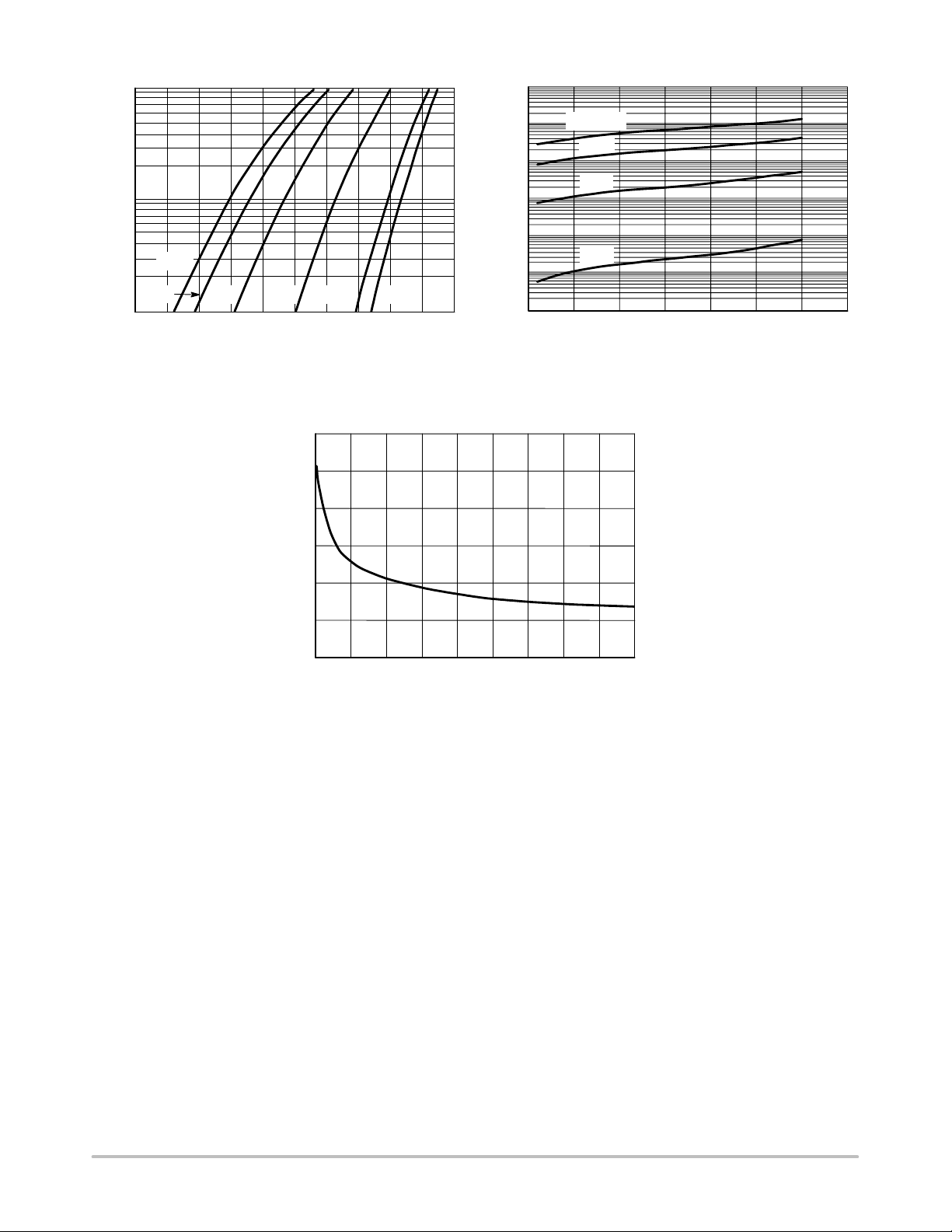
, FORWARD CURRENT (mA)
F
I
10
1.0
0.1
150°C
125°C
0 0.05
1000
T
= 150°C
A
125°C
85°C
25°C
5
10 15 20 25 30 35
, REVERSE VOLTAGE (VOLTS)
V
R
85°C
0.1
0.15
VF, FORWARD VOLTAGE (VOLTS)
0.2
25°C
0.25
-40°C
0.3
0.35
-55°C
0.4
0.45
0.5
, REVERSE CURRENT (µA)
R
I
100
1.0
0.1
0.01
0.001
10
0
Figure 2. Typical Forward Voltage Figure 3. Reverse Current versus Reverse
Voltage
3.0
2.5
2.0
1.5
, CAPACITANCE (pF)
1.0
T
C
0.5
0
0
2.0 4.0
6.0 8.0 10 12 14 16 18
V
, REVERSE VOLTAGE (VOLTS)
R
Figure 4. Typical Capacitance
http://onsemi.com
3
Page 4
J
NOTE 3
RB751V40T1
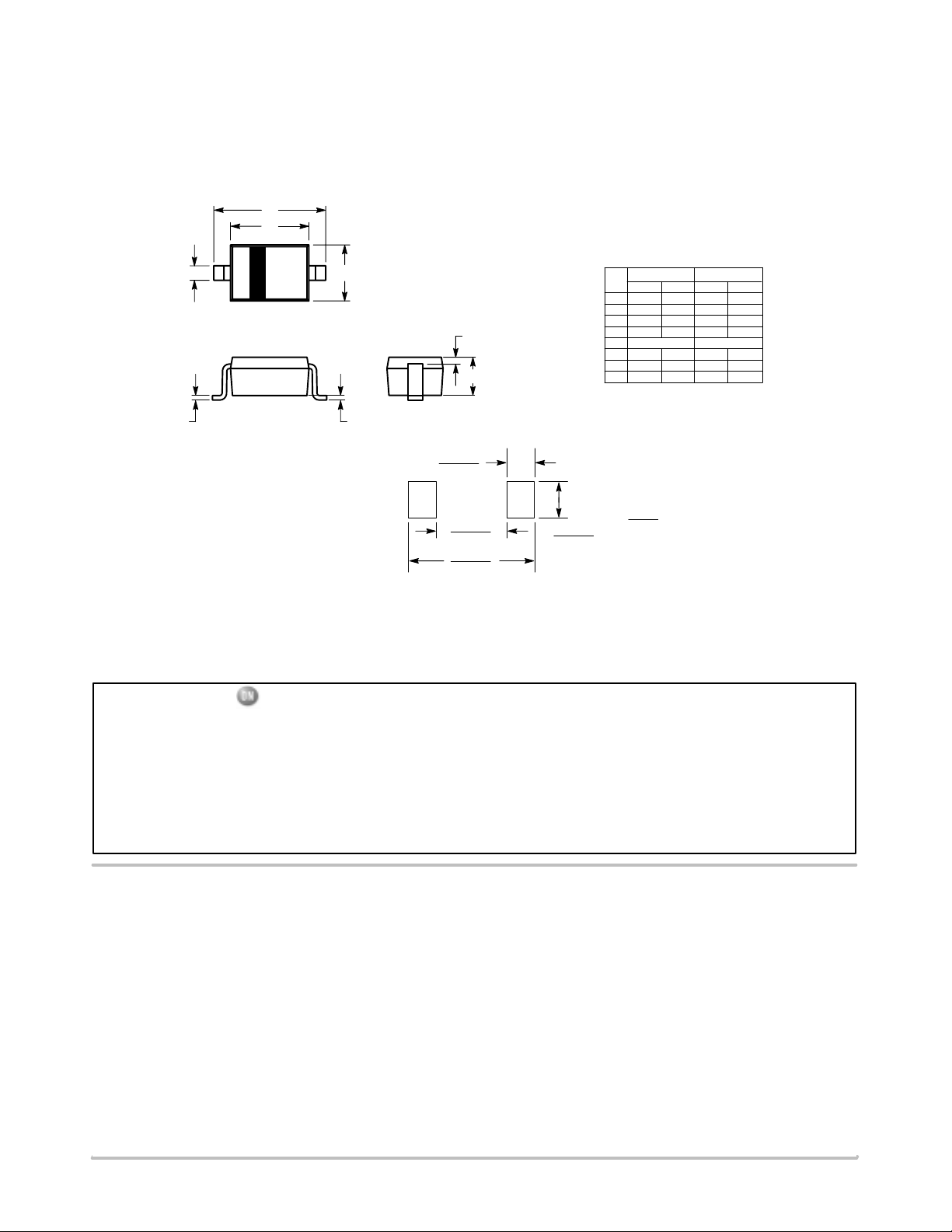
PACKAGE DIMENSIONS
SOD–323
PLASTIC PACKAGE
CASE 477–02
ISSUE B
K
A
1
D
B
2
E
C
H
0.63mm
0.025
NOTES:
1. DIMENSIONING AND TOLERANCING PER ANSI
Y14.5M, 1982.
2. CONTROLLING DIMENSION: MILLIMETERS.
3. LEAD THICKNESS SPECIFIED PER L/F DRAWING
WITH SOLDER PLATING.
DIM MIN MAX MIN MAX
A 1.60 1.80 0.063 0.071
B 1.15 1.35 0.045 0.053
C 0.80 1.00 0.031 0.039
D 0.25 0.40 0.010 0.016
E 0.15 REF 0.006 REF
H 0.00 0.10 0.000 0.004
J 0.089 0.177 0.0035 0.0070
K 2.30 2.70 0.091 0.106
STYLE 1:
PIN 1. CATHODE
2. ANODE
INCHESMILLIMETERS
mm
1.60mm
0.063
2.85mm
0.83mm
0.033
inches
0.112
SOD–323
Soldering Footprint
ON Semiconductor and are trademarks of Semiconductor Components Industries, LLC (SCILLC). SCILLC reserves the right to make changes
without further notice to any products herein. SCILLC makes no warranty, representation or guarantee regarding the suitability of its products for any particular
purpose, nor does SCILLC assume any liability arising out of the application or use of any product or circuit, and specifically disclaims any and all liability,
including without limitation special, consequential or incidental damages. “Typical” parameters which may be provided in SCILLC data sheets and/or
specifications can and do vary in different applications and actual performance may vary over time. All operating parameters, including “Typicals” must be
validated for each customer application by customer’s technical experts. SCILLC does not convey any license under its patent rights nor the rights of others.
SCILLC products are not designed, intended, or authorized for use as components in systems intended for surgical implant into the body, or other applications
intended to support or sustain life, or for any other application in which the failure of the SCILLC product could create a situation where personal injury or
death may occur. Should Buyer purchase or use SCILLC products for any such unintended or unauthorized application, Buyer shall indemnify and hold
SCILLC and its officers, employees, subsidiaries, affiliates, and distributors harmless against all claims, costs, damages, and expenses, and reasonable
attorney fees arising out of, directly or indirectly, any claim of personal injury or death associated with such unintended or unauthorized use, even if such claim
alleges that SCILLC was negligent regarding the design or manufacture of the part. SCILLC is an Equal Opportunity/Affirmative Action Employer.
PUBLICATION ORDERING INFORMATION
NORTH AMERICA Literature Fulfillment:
Literature Distribution Center for ON Semiconductor
P.O. Box 5163, Denver, Colorado 80217 USA
Phone: 303–675–2175 or 800–344–3860 Toll Free USA/Canada
Fax: 303–675–2176 or 800–344–3867 Toll Free USA/Canada
Email: ONlit@hibbertco.com
Fax Response Line: 303–675–2167 or 800–344–3810 Toll Free USA/Canada
N. American Technical Support: 800–282–9855 Toll Free USA/Canada
EUROPE: LDC for ON Semiconductor – European Support
German Phone: (+1) 303–308–7140 (Mon–Fri 2:30pm to 7:00pm CET)
Email: ONlit–german@hibbertco.com
French Phone: (+1) 303–308–7141 (Mon–Fri 2:00pm to 7:00pm CET)
Email: ONlit–french@hibbertco.com
English Phone: (+1) 303–308–7142 (Mon–Fri 12:00pm to 5:00pm GMT)
Email: ONlit@hibbertco.com
EUROPEAN TOLL–FREE ACCESS*: 00–800–4422–3781
*Available from Germany, France, Italy, UK, Ireland
CENTRAL/SOUTH AMERICA:
Spanish Phone: 303–308–7143 (Mon–Fri 8:00am to 5:00pm MST)
Email: ONlit–spanish@hibbertco.com
Toll–Free from Mexico: Dial 01–800–288–2872 for Access –
then Dial 866–297–9322
ASIA/PACIFIC: LDC for ON Semiconductor – Asia Support
Phone: 1–303–675–2121 (Tue–Fri 9:00am to 1:00pm, Hong Kong Time)
Toll Free from Hong Kong & Singapore:
001–800–4422–3781
Email: ONlit–asia@hibbertco.com
JAPAN: ON Semiconductor, Japan Customer Focus Center
4–32–1 Nishi–Gotanda, Shinagawa–ku, Tokyo, Japan 141–0031
Phone: 81–3–5740–2700
Email: r14525@onsemi.com
ON Semiconductor Website: http://onsemi.com
For additional information, please contact your local
Sales Representative.
http://onsemi.com
4
RB751V40T1/D
 Loading...