

Page 1
NVMFS6B85NL
Power MOSFET
100 V, 46 mW, 19 A, Single N−Channel
Features
• Small Footprint (5x6 mm) for Compact Design
• Low R
• Low Q
• NVMFS6B85NLWF − Wettable Flank Option for Enhanced Optical
Inspection
• AEC−Q101 Qualified and PPAP Capable
• These Devices are Pb−Free and are RoHS Compliant
MAXIMUM RATINGS (T
Drain−to−Source Voltage V
Gate−to−Source Voltage V
Continuous Drain
Current R
(Notes 1, 2, 3)
Power Dissipation
(Notes 1, 2)
R
q
JC
Continuous Drain
Current R
(Notes 1, 2, 3)
Power Dissipation
(Notes 1 & 2)
R
q
JA
Pulsed Drain Current
Operating Junction and Storage Temperature TJ, T
Source Current (Body Diode) I
Single Pulse Drain−to−Source Avalanche
Energy (I
Lead Temperature for Soldering Purposes
(1/8″ from case for 10 s)
Stresses exceeding those listed in the Maximum Ratings table may damage the
device. If any of these limits are exceeded, device functionality should not be
assumed, damage may occur and reliability may be affected.
THERMAL RESISTANCE MAXIMUM RATINGS
Junction−to−Case − Steady State
Junction−to−Ambient − Steady State (Note 2)
1. The entire application environment impacts the thermal resistance values shown,
they are not constants and are only valid for the particular conditions noted.
2. Surface−mounted on FR4 board using a 650 mm
3. Maximum current for pulses as long as 1 second is higher but is dependent
on pulse duration and duty cycle.
to Minimize Conduction Losses
DS(on)
and Capacitance to Minimize Driver Losses
G
= 25°C unless otherwise noted)
J
Parameter
q
JC
q
JA
L(pk)
= 1.7 A)
Steady
State
Steady
State
TA = 25°C, t
Parameter Symbol Value Unit
TC = 25°C
TC = 100°C 14
TC = 25°C
TC = 100°C 21
TA = 25°C
TA = 100°C 4.0
TA = 25°C
TA = 100°C 1.75
= 10 ms
p
Symbol Value Unit
DSS
GS
I
D
P
D
I
D
P
D
I
DM
stg
S
E
AS
T
L
R
q
JC
R
q
JA
2
, 2 oz. Cu pad.
100 V
±16 V
19
42
5.6
3.5
93 A
−55 to
+ 175
32 A
116 mJ
260 °C
3.6
43
A
W
A
W
°C
°C/W
www.onsemi.com
V
(BR)DSS
100 V
G (4)
R
MAX ID MAX
DS(ON)
46 mW @ 10 V
72 mW @ 4.5 V
D (5,6)
S (1,2,3)
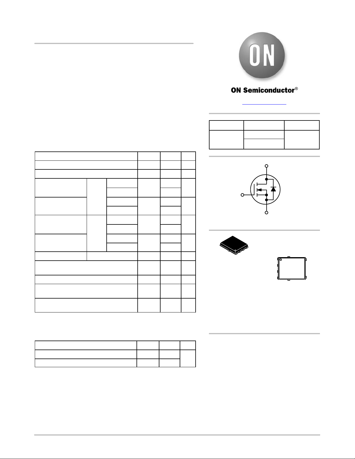
N−CHANNEL MOSFET
19 A
MARKING
DIAGRAM
1
DFN5
(SO−8FL)
CASE 488AA
STYLE 1
6B85NL = NVMFS6B85NL
6B85L W= NVMFS6B85NLWF
A = Assembly Location
Y = Year
W = Work Week
ZZ = Lot Traceability
D
S
6B85xx
S
AYWZZ
S
G
D
D
D
ORDERING INFORMATION
See detailed ordering, marking and shipping information on
page 5 of this data sheet.
© Semiconductor Components Industries, LLC, 2016
August, 2016 − Rev. 0
1 Publication Order Number:
NVMFS6B85NL/D
Page 2
NVMFS6B85NL
ELECTRICAL CHARACTERISTICS (T
Parameter
= 25°C unless otherwise specified)
J
Symbol Test Condition Min Typ Max Unit
OFF CHARACTERISTICS
Drain−to−Source Breakdown Voltage
Drain−to−Source Breakdown Voltage
V
V
Temperature Coefficient
Zero Gate Voltage Drain Current I
Gate−to−Source Leakage Current I
(BR)DSS
(BR)DSS
T
J
DSS
GSS
VGS = 0 V, ID = 250 mA
/
VGS = 0 V,
V
= 80 V
DS
TJ = 25°C 10
TJ = 125°C 250
VDS = 0 V, VGS = 16 V 100 nA
100 V
64
mV/°C
mA
ON CHARACTERISTICS (Note 4)
Gate Threshold Voltage
Threshold Temperature Coefficient V
Drain−to−Source On Resistance R
V
GS(TH)
GS(TH)/TJ
DS(on)
VGS = VDS, ID = 250 mA
VGS = 10 V
VGS = 4.5 V 55 72
ID = 10 A
1.2 2.4 V
−5.2 mV/°C
37 46
mW
CHARGES, CAPACITANCES & GATE RESISTANCE
Input Capacitance
Output Capacitance C
Reverse Transfer Capacitance C
C
ISS
OSS
RSS
VGS = 0 V, f = 1 MHz, VDS = 25 V
480
170
15
pF
VGS = 4.5 V, VDS = 50 V; ID = 10 A 3.8
Total Gate Charge Q
Threshold Gate Charge Q
Gate−to−Source Charge Q
Gate−to−Drain Charge Q
Plateau Voltage V
G(TOT)
G(TH)
GS
GD
GP
VGS = 10 V, VDS = 50 V; ID = 10 A
7.9
1.1
2.4
1.1
4.0 V
nC
SWITCHING CHARACTERISTICS (Note 5)
Turn−On Delay Time
t
d(ON)
Rise Time t
Turn−Off Delay Time t
d(OFF)
Fall Time t
r
f
VGS = 4.5 V, VDS = 50 V,
= 10 A, RG = 2.5 W
I
D
6.9
66.9
12.5
55.9
ns
DRAIN−SOURCE DIODE CHARACTERISTICS
Forward Diode Voltage
Reverse Recovery Time t
Charge Time t
Discharge Time t
Reverse Recovery Charge Q
V
SD
VGS = 0 V,
IS = 10 A
RR
a
b
RR
VGS = 0 V, dIS/dt = 100 A/ms,
I
= 10 A
S
TJ = 25°C 0.88 1.2
TJ = 125°C 0.76
39.4
22.7
16.7
40 nC
V
ns
Product parametric performance is indicated in the Electrical Characteristics for the listed test conditions, unless otherwise noted. Product
performance may not be indicated by the Electrical Characteristics if operated under different conditions.
4. Pulse Test: pulse width v 300 ms, duty cycle v 2%.
5. Switching characteristics are independent of operating junction temperatures.
www.onsemi.com
2
Page 3
NVMFS6B85NL
TYPICAL CHARACTERISTICS
20
VGS = 10 V
to 5 V
15
10
, DRAIN CURRENT (A)
5
D
I
0
0.5 1.5
VDS, DRAIN−TO−SOURCE VOLTAGE (V) VGS, GATE−TO−SOURCE VOLTAGE (V)
4.5 V
2.0
2.5
3.6 V
3.4 V
3.2 V
3.0 V
2.8 V
3.01.00
20
18
16
14
12
10
8
6
, DRAIN CURRENT (A)
D
I
4
2
0
Figure 1. On−Region Characteristics Figure 2. Transfer Characteristics
50
48
46
44
42
40
38
36
34
, DRAIN−TO−SOURCE RESISTANCE (mW)
32
489
DS(on)
R
VGS, GATE−TO−SOURCE VOLTAGE (V) ID, DRAIN CURRENT (A)
61075 10 15
ID = 10 A
= 25°C
T
J
Figure 3. On−Resistance vs. Gate−to−Source
70
65
60
55
50
45
40
35
, DRAIN−TO−SOURCE RESISTANCE (mW)
30
5
DS(on)
R
Figure 4. On−Resistance vs. Drain Current and
Voltage
VDS = 10 V
TJ = 25°C
TJ = 25°C
TJ = 125°C
Gate Voltage
TJ = −55°C
3
VGS = 4.5 V
VGS = 10 V
54210
20
, NORMALIZED DRAIN−TO−
SOURCE RESISTANCE
DS(on)
R
2.4
ID = 10 A
2.2
2.0
1.8
1.6
1.4
1.2
1.0
0.8
0.6
= 10 V
V
GS
50
TJ, JUNCTION TEMPERATURE (°C) VDS, DRAIN−TO−SOURCE VOLTAGE (V)
Figure 5. On−Resistance Variation with
Temperature
10K
1K
100
, LEAKAGE (nA)
DSS
I
10
15012510075250−25−50
1
www.onsemi.com
3
TJ = 150°C
TJ = 125°C
TJ = 85°C
55453525155
75
Figure 6. Drain−to−Source Leakage Current
vs. Voltage
958565175
Page 4
NVMFS6B85NL
TYPICAL CHARACTERISTICS
1000
C
C
100
C
10
C, CAPACITANCE (pF)
1
1000
100
t
r
t
f
t
d(off)
t, TIME (ns)
10
t
d(on)
1
Figure 9. Resistive Switching Time Variation
iss
oss
9
8
7
6
10
rss
5
4
Q
gs
Q
gd
3
VGS = 0 V
= 25°C
T
J
f = 1 MHz
20 30 40 50 60 70 80 90
100
100 4
2
, GATE−TO−SOURCE VOLTAGE (V)
1
GS
0
V
1
2
06
3
5
VDS, DRAIN−TO−SOURCE VOLTAGE (V) Qg, TOTAL GATE CHARGE (nC)
Figure 7. Capacitance Variation Figure 8. Gate−to−Source Voltage vs. Total
Charge
100
TJ = 25°C
10
TJ = 125°C
, SOURCE CURRENT (A)
S
I
1
100101
TJ = −55°C
0.7
V
, SOURCE−TO−DRAIN VOLTAGE (V)
SD
0.9
RG, GATE RESISTANCE (W)
VDS = 50 V
= 10 A
I
D
V
= 4.5 V
GS
Figure 10. Diode Forward Voltage vs. Current
vs. Gate Resistance
TJ = 25°C
= 50 V
V
DS
I
= 10 A
D
7
8
1.31.10.50.3
1000
VGS ≤ 10 V
Single Pulse
TC = 25°C
100
10
, DRAIN CURRENT (A)
1
D
I
0.1
VDS, DRAIN−TO−SOURCE VOLTAGE (V)
Figure 11. Maximum Rated Forward Biased
R
Limit
DS(on)
Thermal Limit
Package Limit
Safe Operating Area
10 ms
500 ms
1 ms
10 ms
100
www.onsemi.com
100
10
T
= 25°C
J(initial)
T
= 100°C
1
, DRAIN CURRENT (A)
PEAK
I
J(initial)
0.1
10001010.1
0.0010.0001
0.01
TAV, TIME IN AVALANCHE (sec)
Figure 12. I
PEAK
vs. T
AV
4
Page 5
100
10
1
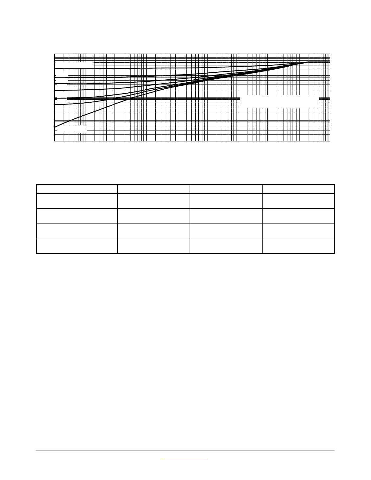
R(t) (°C/W)
0.1
50% Duty Cycle
20%
10%
5%
2%
1%
Single Pulse
NVMFS6B85NL
TYPICAL CHARACTERISTICS
NVMFS6B85NL5x6 SOFL PCB Cu
Area 650 mm
2
PCB Cu thk 2 oz
0.01
0.010.001 1010.00010.00001 0.10.000001
PULSE TIME (sec)
100 1000
Figure 13. Thermal Response
DEVICE ORDERING INFORMATION
Device Marking Package Shipping
NVMFS6B85NLT1G 6B85NL DFN5
(Pb−Free)
NVMFS6B85NLWFT1G 6B85LW DFN5
(Pb−Free, Wettable Flanks)
NVMFS6B85NLT3G 6B85NL DFN5
(Pb−Free)
NVMFS6B85NLWFT3G 6B85LW DFN5
(Pb−Free, Wettable Flanks)
†For information on tape and reel specifications, including part orientation and tape sizes, please refer to our Tape and Reel Packaging
Specifications Brochure, BRD8011/D.
1500 / Tape & Reel
1500 / Tape & Reel
5000 / Tape & Reel
5000 / Tape & Reel
†
www.onsemi.com
5
Page 6
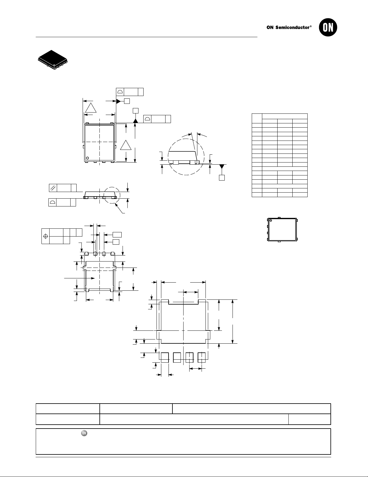
DFN5 5x6, 1.27P
8
s
MECHANICAL CASE OUTLINE
PACKAGE DIMENSIONS
1
SCALE 2:1
2 X
0.20 C
0.10 C
0.10 C
C
0.05
c
PIN 5
(EXPOSED PAD)
D
2
D1
1234
TOP VIEW
SIDE VIEW
8X
b
A0.10 B
L
14
E2
G
D2
BOTTOM VIEW
A
B
E1
E
2
A
DETAIL A
e/2
e
K
M
L1
0.475
2 X
SOLDERING FOOTPRINT*
2X
2X
(SO−8FL)
CASE 488AA
ISSUE N
0.20 C
c
DETAIL A
RECOMMENDED
4.5600.495
2X
1.530
4 X
q
3.200
A1
C
SEATING
PLANE
DATE 25 JUN 201
NOTES:
1. DIMENSIONING AND TOLERANCING PER
ASME Y14.5M, 1994.
2. CONTROLLING DIMENSION: MILLIMETER.
3. DIMENSION D1 AND E1 DO NOT INCLUDE
MOLD FLASH PROTRUSIONS OR GATE
BURRS.
DIM MIN NOM
A1 0.00 −−−
D1 4.70 4.90
D2 3.80 4.00
E1 5.70 5.90
E2 3.45 3.65
L1 0.125 REF
MILLIMETERS
A 0.90 1.00
b 0.33 0.41
c 0.23 0.28
D 5.15
5.00 5.30
E 6.15
6.00 6.30
e 1.27 BSC
G 0.51 0.575
K 1.20 1.35
L 0.51 0.575
M 3.00 3.40
q 0 −−−
_
MAX
1.10
0.05
0.51
0.33
5.10
4.20
6.10
3.85
0.71
1.50
0.71
3.80
12
_
GENERIC
MARKING DIAGRAM*
1
XXXXXX
AYWZZ
XXXXXX = Specific Device Code
A = Assembly Location
Y = Year
W = Work Week
ZZ = Lot Traceability
*This information is generic. Please refer to
device data sheet for actual part marking.
Pb−Free indicator, “G” or microdot “ G”,
may or may not be present. Some product
may not follow the Generic Marking.
4.530
STYLE 1:
PIN 1. SOURCE
2. SOURCE
3. SOURCE
4. GATE
5. DRAIN
STYLE 2:
PIN 1. ANODE
2. ANODE
3. ANODE
4. NO CONNECT
5. CATHODE
2X
0.905
0.965
1.000
4X
4X
0.750
1
DIMENSIONS: MILLIMETERS
1.330
1.270
PITCH
*For additional information on our Pb−Free strategy and soldering
details, please download the ON Semiconductor Soldering and
Mounting Techniques Reference Manual, SOLDERRM/D.
DOCUMENT NUMBER:
DESCRIPTION:
ON Semiconductor and are trademarks of Semiconductor Components Industries, LLC dba ON Semiconductor or its subsidiaries in the United States and/or other countries.
ON Semiconductor reserves the right to make changes without further notice to any products herein. ON Semiconductor makes no warranty, representation or guarantee regarding
the suitability of its products for any particular purpose, nor does ON Semiconductor assume any liability arising out of the application or use of any product or circuit, and specifically
disclaims any and all liability, including without limitation special, consequential or incidental damages. ON Semiconductor does not convey any license under its patent rights nor the
rights of others.
© Semiconductor Components Industries, LLC, 2018
98AON14036D
DFN5 5x6, 1.27P (SO−8FL)
Electronic versions are uncontrolled except when accessed directly from the Document Repository.
Printed versions are uncontrolled except when stamped “CONTROLLED COPY” in red.
PAGE 1 OF 1
www.onsemi.com
Page 7
ON Semiconductor and are trademarks of Semiconductor Components Industries, LLC dba ON Semiconductor or its subsidiaries in the United States and/or other countries.
ON Semiconductor owns the rights to a number of patents, trademarks, copyrights, trade secrets, and other intellectual property. A listing of ON Semiconductor ’s product/patent
coverage may be accessed at www.onsemi.com/site/pdf/Patent−Marking.pdf
ON Semiconductor makes no warranty, representation or guarantee regarding the suitability of its products for any particular purpose, nor does ON Semiconductor assume any liability
arising out of the application or use of any product or circuit, and specifically disclaims any and all liability, including without limitation special, consequential or incidental damages.
Buyer is responsible for its products and applications using ON Semiconductor products, including compliance with all laws, regulations and safety requirements or standards,
regardless of any support or applications information provided by ON Semiconductor. “Typical” parameters which may be provided in ON Semiconductor data sheets and/or
specifications can and do vary in different applications and actual performance may vary over time. All operating parameters, including “Typicals” must be validated for each customer
application by customer’s technical experts. ON Semiconductor does not convey any license under its patent rights nor the rights of others. ON Semiconductor products are not
designed, intended, or authorized for use as a critical component in life support systems or any FDA Class 3 medical devices or medical devices with a same or similar classification
in a foreign jurisdiction or any devices intended for implantation in the human body. Should Buyer purchase or use ON Semiconductor products for any such unintended or unauthorized
application, Buyer shall indemnify and hold ON Semiconductor and its officers, employees, subsidiaries, affiliates, and distributors harmless against all claims, costs, damages, and
expenses, and reasonable attorney fees arising out of, directly or indirectly, any claim of personal injury or death associated with such unintended or unauthorized use, even if such
claim alleges that ON Semiconductor was negligent regarding the design or manufacture of the part. ON Semiconductor is an Equal Opportunity/Affirmative Action Employer. This
literature is subject to all applicable copyright laws and is not for resale in any manner.
. ON Semiconductor reserves the right to make changes without further notice to any products herein.
PUBLICATION ORDERING INFORMATION
LITERATURE FULFILLMENT:
Email Requests to: orderlit@onsemi.com
ON Semiconductor Website: www.onsemi.com
TECHNICAL SUPPORT
North American Technical Support:
Voice Mail: 1 800−282−9855 Toll Free USA/Canada
Phone: 011 421 33 790 2910
Europe, Middle East and Africa Technical Support:
Phone: 00421 33 790 2910
For additional information, please contact your local Sales Representative
◊
www.onsemi.com
1
 Loading...