

Page 1
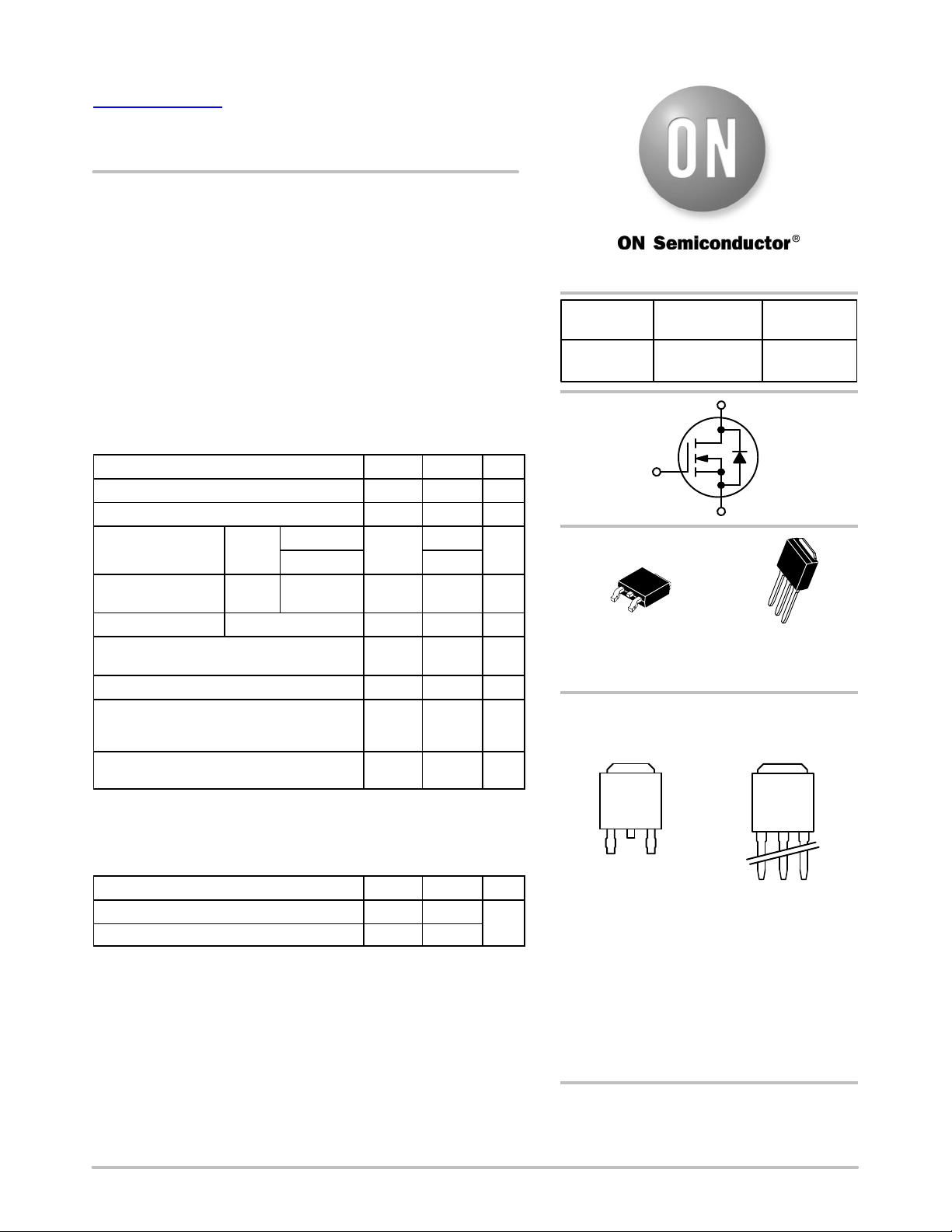
MOSFET – Power,
N-Channel
100 V, 17 A, 81 mW
NTD6416AN, NVD6416AN
Features
• Low R
• High Current Capability
• 100% Avalanche Tested
• NVD Prefix for Automotive and Other Applications Requiring
• These Devices are Pb−Free and are RoHS Compliant
DS(on)
Unique Site and Control Change Requirements; AEC−Q101
Qualified and PPAP Capable
http://onsemi.com
I
V
(BR)DSS
100 V 81 mW @ 10 V 17 A
R
DS(on)
MAX
D
D
(Note 1)
MAX
MAXIMUM RATINGS (T
Parameter
Drain−to−Source Voltage V
Gate−to−Source Voltage − Continuous V
Continuous Drain
Current
Power Dissipation Steady
Pulsed Drain Current
Operating and Storage Temperature Range TJ, T
Source Current (Body Diode) I
Single Pulse Drain−to−Source Avalanche
Energy (V
I
L(pk)
Lead Temperature for Soldering
Purposes, 1/8″ from Case for 10 Seconds
Stresses exceeding those listed in the Maximum Ratings table may damage the
device. If any of these limits are exceeded, device functionality should not be
assumed, damage may occur and reliability may be affected.
= 50 Vdc, VGS = 10 Vdc,
DD
= 17 A, L = 0.3 mH, RG = 25 W)
= 25°C unless otherwise noted)
J
Steady
State
State
TC = 25°C
TC = 100°C 11
TC = 25°C P
tp = 10 ms
Symbol Value Unit
stg
100 V
±20 V
17
71 W
62 A
−55 to
+175
17 A
43 mJ
260 °C
A
°C
I
E
DSS
GS
I
D
D
DM
S
AS
T
L
THERMAL RESISTANCE RATINGS
Parameter Symbol Max Unit
Junction−to−Case (Drain) Steady State
Junction−to−Ambient (Note 1)
1. Surface mounted on FR4 board using 1 sq in pad size,
(Cu Area 1.127 sq in [2 oz] including traces).
R
q
JC
R
q
JA
2.1
40
°C/W
G
2
1
3
DPAK
CASE 369AA
STYLE 2
4
N−Channel
S
1
2
IPAK
CASE 369D
STYLE 2
4
3
MARKING DIAGRAM
& PIN ASSIGNMENTS
4 Drain
AYWW6416ANG
1
Gate
Drain
A = Assembly Location*
Y = Year
WW = Work Week
6416AN = Device Code
G = Pb−Free Package
* The Assembly Location code (A) is front side
optional. In cases where the Assembly Location is
stamped in the package, the front side assembly
code may be blank.
3
2
Source
Gate
1
4 Drain
AYWW6416ANG
3
Source
2
Drain
© Semiconductor Components Industries, LLC, 2014
April, 2020 − Rev. 4
ORDERING INFORMATION
See detailed ordering and shipping information on page 5 of
this data sheet.
1 Publication Order Number:
NTD6416AN/D
Page 2
NTD6416AN, NVD6416AN
ELECTRICAL CHARACTERISTICS (T
Parameter
= 25°C unless otherwise noted)
J
Symbol Test Condition Min Typ Max Unit
OFF CHARACTERISTICS
Drain−to−Source Breakdown Voltage
Drain−to−Source Breakdown Voltage
V
(BR)DSS
V
(BR)DSS/TJ
VGS = 0 V, ID = 250 mA
100 V
112 mV/°C
Temperature Coefficient
Zero Gate Voltage Drain Current I
Gate−to−Source Leakage Current I
DSS
GSS
VGS = 0 V,
V
= 100 V
DS
VDS = 0 V, VGS = "20 V ±100 nA
TJ = 25°C 1.0 mA
TJ = 125°C 10
ON CHARACTERISTICS (Note 3)
Gate Threshold Voltage
Negative Threshold Temperature
V
GS(TH)
V
GS(TH)/TJ
VGS = VDS, ID = 250 mA
2.0 4.0 V
7.7 mV/°C
Coefficient
Drain−to−Source On−Resistance R
Forward Transconductance g
DS(on)
FS
VGS = 10 V, ID = 17 A 73 81
VDS = 5 V, ID = 10 A 12
mW
S
CHARGES, CAPACITANCES AND GATE RESISTANCE
Input Capacitance
C
Output Capacitance C
Reverse Transfer Capacitance C
Total Gate Charge Q
G(TOT)
Threshold Gate Charge Q
Gate−to−Source Charge Q
Gate−to−Drain Charge Q
Plateau Voltage V
Gate Resistance R
ISS
OSS
RSS
G(TH)
GS
GD
GP
G
VGS = 0 V, f = 1.0 MHz, VDS = 25 V
VGS = 10 V, VDS = 80 V, ID = 17 A
620
110
50
20
1.0
3.6
10
5.8 V
2.4
pF
nC
W
SWITCHING CHARACTERISTICS (Note 4)
Turn−On Delay Time
t
Rise Time t
Turn−Off Delay Time t
Fall Time t
d(on)
r
d(off)
f
VGS = 10 V, VDD = 80 V,
= 17 A, RG = 6.1 W
I
D
9.2
22
24
20
ns
DRAIN−SOURCE DIODE CHARACTERISTICS
Forward Diode Voltage
Reverse Recovery Time t
Charge Time t
Discharge Time t
Reverse Recovery Charge Q
V
SD
rr
a
b
RR
VGS = 0 V, IS = 17 A
VGS = 0 V, dIS/dt = 100 A/ms,
I
= 17 A
S
TJ = 25°C 0.85 1.2
TJ = 125°C 0.7
56
41
15
135 nC
V
ns
Product parametric performance is indicated in the Electrical Characteristics for the listed test conditions, unless otherwise noted. Product
performance may not be indicated by the Electrical Characteristics if operated under different conditions.
2. Surface mounted on FR4 board using 1 in sq pad size (Cu area = 1.127 in sq [1 oz] including traces).
3. Pulse Test: Pulse Width ≤ 300 ms, Duty Cycle ≤ 2%.
4. Switching characteristics are independent of operating junction temperatures.
http://onsemi.com
2
Page 3
NTD6416AN, NVD6416AN
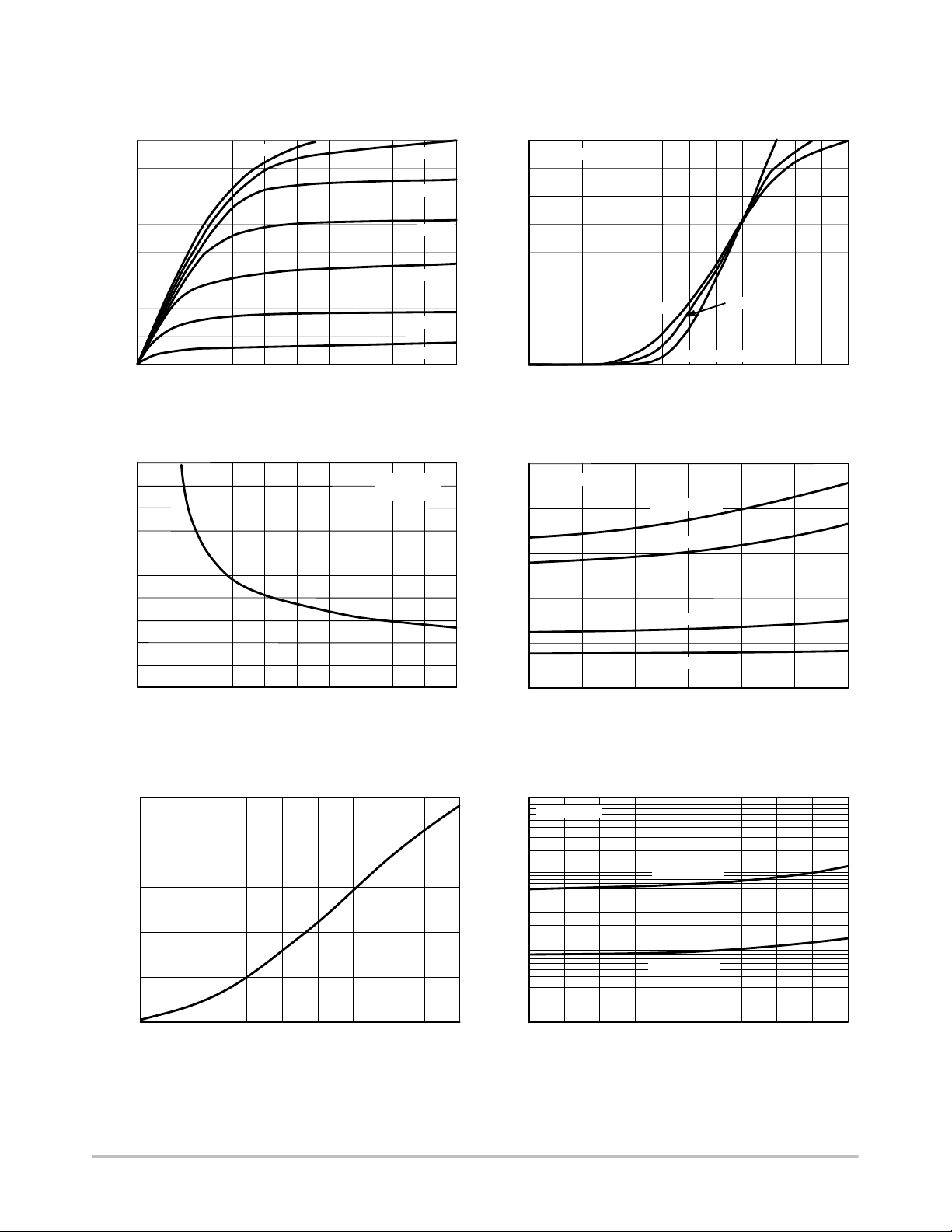
TYPICAL CHARACTERISTICS
40
TJ = 25°C
30
10 V
7.5 V
6.5 V
6.0 V
20
5.5 V
, DRAIN CURRENT (A)
10
D
I
0
5.0 V
4.5 V
0246810
V
, DRAIN−TO−SOURCE VOLTAGE (V)
DS
Figure 1. On−Region Characteristics
0.11
ID = 17 A
= 25°C
T
0.10
0.09
J
40
VDS w 10 V
35
30
25
20
15
, DRAIN CURRENT (A)
10
D
I
TJ = 125°C
TJ = 25°C
5
0
TJ = −55°C
2345678
V
, GATE−TO−SOURCE VOLTAGE (V)
GS
Figure 2. Transfer Characteristics
0.25
VGS = 10 V
0.20
0.15
TJ = 175°C
TJ = 125°C
0.08
0.07
, DRAIN−TO−SOURCE RESISTANCE (W)
0.06
5678910
DS(on)
R
, GATE−TO−SOURCE VOLTAGE (V)
V
GS
Figure 3. On−Region versus Gate Voltage
3
ID = 17 A
= 10 V
V
GS
2.5
2
1.5
(NORMALIZED)
1
, DRAIN−TO−SOURCE RESISTANCE
0.5
−50 −25 0 25 50 75 100 125 150 175
DS(on)
R
T
, JUNCTION TEMPERATURE (°C)
J
Figure 5. On−Resistance Variation with
Temperature
0.10
TJ = 25°C
0.05
, DRAIN−TO−SOURCE RESISTANCE (W)
TJ = −55°C
0.00
DS(on)
R
10 20812
I
, DRAIN CURRENT (A)
D
14 16 18
Figure 4. On−Resistance versus Drain Current
and Gate Voltage
10000
, LEAKAGE (nA)
DSS
I
VGS = 0 V
1000
TJ = 150°C
100
TJ = 125°C
10
10 20 30 40 50 60 70 80 90 100
, DRAIN−TO−SOURCE VOLTAGE (V)
V
DS
Figure 6. Drain−to−Source Leakage Current
versus Voltage
http://onsemi.com
3
Page 4

NTD6416AN, NVD6416AN
TYPICAL CHARACTERISTICS
1200
1000
TJ = 25°C
= 0 V
V
GS
800
C
600
iss
400
C, CAPACITANCE (pF)
200
C
C
rss
0
oss
0 20406080100
V
, DRAIN−TO−SOURCE VOLTAGE (V)
DS
Figure 7. Capacitance Variation
1000
VDS = 80 V
= 17 A
I
D
V
= 10 V
GS
t
100
d(off)
t
r
10
8
V
DS
Q
gs
6
Q
T
V
GS
Q
gd
4
2
, GATE−TO−SOURCE VOLTAGE (V)
GS
V
0
ID = 17 A
= 25°C
T
J
0 5 10 15 20
Qg, TOTAL GATE CHARGE (nC)
Figure 8. Gate−to−Source Voltage and
Drain−to−Source Voltage versus Total Charge
20
TJ = 25°C
= 0 V
V
GS
15
10
100
80
60
40
20
0
, DRAIN−TO−SOURCE VOLTAGE (V)
DS
V
t, TIME (ns)
10
1
1 10 100
t
f
, GATE RESISTANCE (W)
R
G
Figure 9. Resistive Switching Time Variation
versus Gate Resistance
1000
100
10 ms
10
VGS = 10 V
SINGLE PULSE
, DRAIN CURRENT (A)
D
I
TC = 25°C
1
R
DS(on)
LIMIT
100 ms
1 ms
10 ms
dc
THERMAL LIMIT
0.1
PACKAGE LIMIT
1 10 100 1000
VDS, DRAIN−TO−SOURCE VOLTAGE (V)
Figure 11. Maximum Rated Forward Biased
Safe Operating Area
t
d(on)
5
, SOURCE CURRENT (A)
S
I
0
0.5 0.6 0.7 0.8 0.9 1.0
, SOURCE−TO−DRAIN VOLTAGE (V)
V
SD
Figure 10. Diode Forward Voltage versus
Current
50
ID = 17 A
40
30
20
10
AVALANCHE ENERGY (mJ)
0
25 50 75 100 125 150 175
TJ, STARTING JUNCTION TEMPERATURE
Figure 12. Maximum Avalanche Energy versus
Starting Junction Temperature
http://onsemi.com
4
Page 5

NTD6416AN, NVD6416AN
TYPICAL CHARACTERISTICS
10
1
D = 0.5
0.2
0.1
0.1
0.05
0.02
R(t) (°C/W)
ORDERING INFORMATION
NTD6416ANT4G DPAK
NTD6416AN−1G IPAK
NVD6416ANT4G* DPAK
NVD6416ANT4G−VF01* DPAK
†For information on tape and reel specifications, including part orientation and tape sizes, please refer to our Tape and Reel Packaging
Specification Brochure, BRD8011/D.
*NVD Prefix for Automotive and Other Applications Requiring Unique Site and Control Change Requirements; AEC−Q101 Qualified and PPAP
Capable.
0.01
0.01
SINGLE PULSE
0.001
0.000001 0.00001 0.0001 0.001 0.01 0.1 1 10
t, PULSE TIME (s)
Figure 13. Thermal Response
Device Package Shipping†
(Pb−Free)
(Pb−Free)
(Pb−Free)
(Pb−Free)
2500 / Tape & Reel
75 Units / Rail
2500 / Tape & Reel
2500 / Tape & Reel
http://onsemi.com
5
Page 6

MECHANICAL CASE OUTLINE
PACKAGE DIMENSIONS
IPAK
CASE 369D−01
ISSUE C
DATE 15 DEC 2010
SCALE 1:1
STYLE 1:
PIN 1. BASE
STYLE 5:
PIN 1. GATE
V
S
−T−
SEATING
PLANE
F
2. COLLECTOR
3. EMITTER
4. COLLECTOR
2. ANODE
3. CATHODE
4. ANODE
B
R
4
123
G
STYLE 2:
PIN 1. GATE
2. DRAIN
3. SOURCE
4. DRAIN
STYLE 6:
PIN 1. MT1
2. MT2
3. GATE
4. MT2
A
K
3 PL
D
0.13 (0.005) T
STYLE 3:
PIN 1. ANODE
STYLE 7:
PIN 1. GATE
C
J
M
2. CATHODE
3. ANODE
4. CATHODE
2. COLLECTOR
3. EMITTER
4. COLLECTOR
E
H
STYLE 4:
PIN 1. CATHODE
2. ANODE
3. GATE
4. ANODE
NOTES:
1. DIMENSIONING AND TOLERANCING PER
ANSI Y14.5M, 1982.
2. CONTROLLING DIMENSION: INCH.
Z
DIM MIN MAX MIN MAX
A 0.235 0.245 5.97 6.35
B 0.250 0.265 6.35 6.73
C 0.086 0.094 2.19 2.38
D 0.027 0.035 0.69 0.88
E 0.018 0.023 0.46 0.58
F 0.037 0.045 0.94 1.14
0.090 BSC 2.29 BSC
G
H 0.034 0.040 0.87 1.01
J 0.018 0.023 0.46 0.58
K 0.350 0.380 8.89 9.65
R 0.180 0.215 4.45 5.45
S 0.025 0.040 0.63 1.01
V 0.035 0.050 0.89 1.27
Z 0.155 −−− 3.93 −−−
MILLIMETERSINCHES
MARKING
DIAGRAMS
Integrated
Discrete
YWW
xxxxxxxx
Circuits
xxxxx
ALYWW
x
xxxxxxxxx = Device Code
A = Assembly Location
lL = Wafer Lot
Y = Year
WW = Work Week
DOCUMENT NUMBER:
DESCRIPTION:
ON Semiconductor and are trademarks of Semiconductor Components Industries, LLC dba ON Semiconductor or its subsidiaries in the United States and/or other countries.
ON Semiconductor reserves the right to make changes without further notice to any products herein. ON Semiconductor makes no warranty, representation or guarantee regarding
the suitability of its products for any particular purpose, nor does ON Semiconductor assume any liability arising out of the application or use of any product or circuit, and specifically
disclaims any and all liability, including without limitation special, consequential or incidental damages. ON Semiconductor does not convey any license under its patent rights nor the
rights of others.
98AON10528D
IPAK (DPAK INSERTION MOUNT)
Electronic versions are uncontrolled except when accessed directly from the Document Repository.
Printed versions are uncontrolled except when stamped “CONTROLLED COPY” in red.
PAGE 1 OF 1
© Semiconductor Components Industries, LLC, 2019
www.onsemi.com
Page 7

MECHANICAL CASE OUTLINE
PACKAGE DIMENSIONS
2
1
3
SCALE 1:1
L3
L4
b2
e
STYLE 1:
PIN 1. BASE
2. COLLECTOR
3. EMITTER
4. COLLECTOR
4
E
b3
4
12 3
A
B
D
b
0.005 (0.13) C
STYLE 2:
PIN 1. GATE
2. DRAIN
3. SOURCE
4. DRAIN
DETAIL A
M
STYLE 3:
PIN 1. ANODE
DPAK (SINGLE GUAGE)
CASE 369AA−01
ISSUE B
C
A
c2
H
c
GAUGE
L2
PLANE
L
L1
DETAIL A
ROTATED 90 CW5
STYLE 4:
2. CATHODE
3. ANODE
4. CATHODE
PIN 1. CATHODE
A1
2. ANODE
3. GATE
4. ANODE
DATE 03 JUN 2010
NOTES:
1. DIMENSIONING AND TOLERANCING PER ASME
Y14.5M, 1994.
2. CONTROLLING DIMENSION: INCHES.
3. THERMAL PAD CONTOUR OPTIONAL WITHIN DIMENSIONS b3, L3 and Z.
4. DIMENSIONS D AND E DO NOT INCLUDE MOLD
FLASH, PROTRUSIONS, OR BURRS. MOLD
FLASH, PROTRUSIONS, OR GATE BURRS SHALL
NOT EXCEED 0.006 INCHES PER SIDE.
Z
H
SEATING
C
PLANE
5. DIMENSIONS D AND E ARE DETERMINED AT THE
OUTERMOST EXTREMES OF THE PLASTIC BODY.
6. DATUMS A AND B ARE DETERMINED AT DATUM
PLANE H.
DIM MIN MAX MIN MAX
A 0.086 0.094 2.18 2.38
A1 0.000 0.005 0.00 0.13
b 0.025 0.035 0.63 0.89
b2 0.030 0.045 0.76 1.14
b3 0.180 0.215 4.57 5.46
c 0.018 0.024 0.46 0.61
c2 0.018 0.024 0.46 0.61
D 0.235 0.245 5.97 6.22
E 0.250 0.265 6.35 6.73
e 0.090 BSC 2.29 BSC
H 0.370 0.410 9.40 10.41
L 0.055 0.070 1.40 1.78
L1 0.108 REF 2.74 REF
L2 0.020 BSC 0.51 BSC
L3 0.035 0.050 0.89 1.27
L4 −−− 0.040 −−− 1.01
Z 0.155 −−− 3.93 −−−
MILLIMETERSINCHES
GENERIC
MARKING DIAGRAM*
STYLE 5:
PIN 1. GATE
2. ANODE
3. CATHODE
4. ANODE
STYLE 6:
PIN 1. MT1
2. MT2
3. GATE
4. MT2
STYLE 7:
PIN 1. GATE
2. COLLECTOR
3. EMITTER
4. COLLECTOR
SOLDERING FOOTPRINT*
6.20
0.244
5.80
0.228
*For additional information on our Pb−Free strategy and soldering
details, please download the ON Semiconductor Soldering and
Mounting Techniques Reference Manual, SOLDERRM/D.
DOCUMENT NUMBER:
DESCRIPTION:
98AON13126D
DPAK (SINGLE GAUGE)
2.58
0.102
3.00
0.118
0.063
1.60
SCALE 3:1
6.17
0.243
ǒ
inches
XXXXXXG
ALYWW
YWW
XXX
XXXXXG
DiscreteIC
XXXXXX = Device Code
A = Assembly Location
L = Wafer Lot
Y = Year
WW = Work Week
G = Pb−Free Package
*This information is generic. Please refer
to device data sheet for actual part
mm
Ǔ
Electronic versions are uncontrolled except when accessed directly from the Document Repository.
Printed versions are uncontrolled except when stamped “CONTROLLED COPY” in red.
marking.
PAGE 1 OF 1
ON Semiconductor and are trademarks of Semiconductor Components Industries, LLC dba ON Semiconductor or its subsidiaries in the United States and/or other countries.
ON Semiconductor reserves the right to make changes without further notice to any products herein. ON Semiconductor makes no warranty, representation or guarantee regarding
the suitability of its products for any particular purpose, nor does ON Semiconductor assume any liability arising out of the application or use of any product or circuit, and specifically
disclaims any and all liability, including without limitation special, consequential or incidental damages. ON Semiconductor does not convey any license under its patent rights nor the
rights of others.
© Semiconductor Components Industries, LLC, 2019
www.onsemi.com
Page 8

ON Semiconductor and are trademarks of Semiconductor Components Industries, LLC dba ON Semiconductor or its subsidiaries in the United States and/or other countries.
ON Semiconductor owns the rights to a number of patents, trademarks, copyrights, trade secrets, and other intellectual property. A listing of ON Semiconductor’s product/patent
coverage may be accessed at www.onsemi.com/site/pdf/Patent−Marking.pdf
ON Semiconductor makes no warranty, representation or guarantee regarding the suitability of its products for any particular purpose, nor does ON Semiconductor assume any liability
arising out of the application or use of any product or circuit, and specifically disclaims any and all liability, including without limitation special, consequential or incidental damages.
Buyer is responsible for its products and applications using ON Semiconductor products, including compliance with all laws, regulations and safety requirements or standards,
regardless of any support or applications information provided by ON Semiconductor. “Typical” parameters which may be provided in ON Semiconductor data sheets and/or
specifications can and do vary in different applications and actual performance may vary over time. All operating parameters, including “Typicals” must be validated for each customer
application by customer’s technical experts. ON Semiconductor does not convey any license under its patent rights nor the rights of others. ON Semiconductor products are not
designed, intended, or authorized for use as a critical component in life support systems or any FDA Class 3 medical devices or medical devices with a same or similar classification
in a foreign jurisdiction or any devices intended for implantation in the human body. Should Buyer purchase or use ON Semiconductor products for any such unintended or unauthorized
application, Buyer shall indemnify and hold ON Semiconductor and its officers, employees, subsidiaries, affiliates, and distributors harmless against all claims, costs, damages, and
expenses, and reasonable attorney fees arising out of, directly or indirectly, any claim of personal injury or death associated with such unintended or unauthorized use, even if such
claim alleges that ON Semiconductor was negligent regarding the design or manufacture of the part. ON Semiconductor is an Equal Opportunity/Affirmative Action Employer. This
literature is subject to all applicable copyright laws and is not for resale in any manner.
. ON Semiconductor reserves the right to make changes without further notice to any products herein.
PUBLICATION ORDERING INFORMATION
LITERATURE FULFILLMENT:
Email Requests to: orderlit@onsemi.com
ON Semiconductor Website: www.onsemi.com
TECHNICAL SUPPORT
North American Technical Support:
Voice Mail: 1 800−282−9855 Toll Free USA/Canada
Phone: 011 421 33 790 2910
Europe, Middle East and Africa Technical Support:
Phone: 00421 33 790 2910
For additional information, please contact your local Sales Representative
◊
www.onsemi.com
1
Page 9

Mouser Electronics
Authorized Distributor
Click to View Pricing, Inventory, Delivery & Lifecycle Information:
ON Semiconductor:
NTD6416AN-1G NTD6416ANT4G NVD6416ANT4G NVD6416ANT4G-VF01
 Loading...