

NTA4001N, NVA4001N
MOSFET – Single,
N-Channel, Gate ESD
Protection, Small Signal,
SC-75
20 V, 238 mA
Features
• Low Gate Charge for Fast Switching
• Small 1.6 x 1.6 mm Footprint
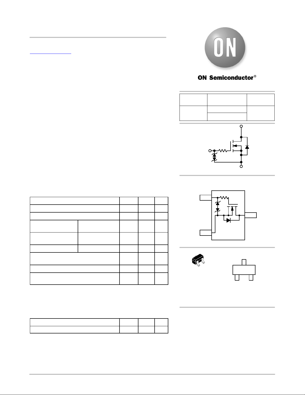
• ESD Protected Gate
• AEC−Q101 Qualified and PPAP Capable − NVA4001N
• These Devices are Pb−Free and are RoHS Compliant
http://onsemi.com
V
(BR)DSS
20 V 238 mA
R
DS(on)
Typ @ V
1.5 W @ 4.5 V
2.2 W @ 2.5 V
GS
3
ID MAX
(Note 1)
Applications
• Power Management Load Switch
• Level Shift
• Portable Applications such as Cell Phones, Media Players,
Digital Cameras, PDA’s, Video Games, Hand Held Computers, etc.
MAXIMUM RATINGS (T
Parameter
Drain−to−Source Voltage V
Gate−to−Source Voltage V
Continuous Drain
Current (Note 1)
Power Dissipation
(Note 1)
Pulsed Drain Current
Operating Junction and Storage Temperature TJ,
Continuous Source Current (Body Diode) I
Lead Temperature for Soldering Purposes
(1/8” from case for 10 s)
Stresses exceeding Maximum Ratings may damage the device. Maximum
Ratings are stress ratings only. Functional operation above the Recommended
Operating Conditions is not implied. Extended exposure to stresses above the
Recommended Operating Conditions may affect device reliability.
= 25°C unless otherwise stated)
J
Symbol Value Unit
DSS
GS
Steady State = 25°C I
Steady State = 25°C P
tP v 10 ms
T
I
DM
STG
SD
T
D
D
L
20 V
±10 V
238 mA
300 mW
714 mA
−55 to
150
238 mA
260 °C
°C
1
PIN CONNECTIONS
Gate31
Source
SC−75 / SOT−416
CASE 463
2
3
2
1
STYLE 5
TF = Specific Device Code
M = Date Code
G = Pb−Free Package
(Note: Microdot may be in either location)
N−Channel
SC−75 (3−Leads)
(Top View)
MARKING DIAGRAM
TF MG
1
2
Drain
3
G
2
THERMAL RESISTANCE RATINGS
Parameter Symbol Max Unit
Junction−to−Ambient – Steady State (Note 1)
1. Surface−mounted on FR4 board using 1 in sq. pad size (Cu area = 1.127 in sq.
[1 oz] including traces).
© Semiconductor Components Industries, LLC, 2011
May, 2019 − Rev. 2
R
q
JA
416 °C/W
1 Publication Order Number:
ORDERING INFORMATION
See detailed ordering and shipping information in the package
dimensions section on page 4 of this data sheet.
NTA4001N/D
NTA4001N, NVA4001N
ELECTRICAL CHARACTERISTICS (T
Parameter
= 25°C unless otherwise specified)
J
Symbol Test Condition Min Typ Max Unit
OFF CHARACTERISTICS
Drain−to−Source Breakdown Voltage
Zero Gate Voltage Drain Current I
Gate−to−Source Leakage Current I
V
(BR)DSS
DSS
GSS
VGS = 0 V, ID = 100 mA
VGS = 0 V, VDS = 20 V 1.0
VDS = 0 V, VGS = ±10 V ±100
ON CHARACTERISTICS (Note 2)
Gate Threshold Voltage
Drain−to−Source On Resistance R
V
GS(TH)
DS(on)
VDS = 3 V, ID = 100 mA
VGS = 4.5 V, ID = 10 mA 1.5 3.0
VGS = 2.5 V, ID = 10 mA 2.2 3.5
Forward Transconductance g
FS
CAPACITANCES
Input Capacitance
Output Capacitance C
Reverse Transfer Capacitance C
C
ISS
OSS
RSS
SWITCHING CHARACTERISTICS (Note 3)
Turn−On Delay Time
Rise Time t
Turn−Off Delay Time t
Fall Time t
t
d(ON)
r
d(OFF)
f
VGS = 4.5 V, VDS = 5 V,
I
DRAIN−SOURCE DIODE CHARACTERISTICS
Forward Diode Voltage
V
SD
2. Pulse Test: pulse width v 300 ms, duty cycle v 2%.
3. Switching characteristics are independent of operating junction temperatures.
20 V
mA
mA
0.5 1.0 1.5 V
W
VDS = 3 V, ID = 10 mA 80 mS
11.5 20
VDS = 5 V, f = 1 MHz,
V
= 0 V
GS
10 15
pF
3.5 6.0
13 ns
15
= 10 mA, RG = 10 W
D
98
ns
60
VGS = 0 V, IS = 10 mA 0.66 0.8 V
http://onsemi.com
2
 Loading...