

ON Semiconductor NUP4201MR6 Technical data
查询NUP4201MR6供应商
NUP4201MR6
Low Capacitance TSOP−6
Diode−TVS Array for High
Speed Data Lines
Protection
The NUP4201MR6 transient voltage suppressor is designed to
protect high speed data lines from ESD, EFT, and lighting.
Features:
• Low Capacitance (3 pF Maximum Between I/O Lines)
• ESD Rating of Class 3B (Exceeding 8 kV) per Human Body model
and Class C (Exceeding 400 V) per Machine Model
• Protection for the Following IEC Standards:
IEC 61000−4−2 (ESD) 15 kV (air) 8 kV (contact)
IEC 61000−4−4 (EFT) 40 A (5/50 ns)
IEC 61000−4−5 (lighting) 23 A (8/20 s)
• UL Flammability Rating of 94 V−0
• Pb−Free Package is Available
T ypical Applications:
• High Speed Communication Line Protection
• USB 1.1 and 2.0 Power and Data Line Protection
• Digital Video Interface (DVI)
• Monitors and Flat Panel Displays
MAXIMUM RATINGS (T
Rating
Peak Power Dissipation
8 x 20 S @ TA = 25°C (Note 1)
Operating Junction Temperature Range T
Storage Temperature Range T
Lead Solder Temperature −
Maximum (10 Seconds)
Human Body Model (HBM)
Machine Model (MM)
IEC 61000−4−2 Air (ESD)
IEC 61000−4−2 Contact (ESD)
Maximum ratings are those values beyond which device damage can occur.
Maximum ratings applied to the device are individual stress limit values (not
normal operating conditions) and are not valid simultaneously. If these limits are
exceeded, device functional operation is not implied, damage may occur and
reliability may be affected.
1. Non−repetitive current pulse per Figure 1 (Pin 5 to Pin 2)
= 25°C unless otherwise noted)
J
Symbol Value Unit
P
pk
J
stg
T
L
ESD 16000
500 W
−40 to +125 °C
−55 to +150 °C
235 °C
V
400
20000
20000
http://onsemi.com
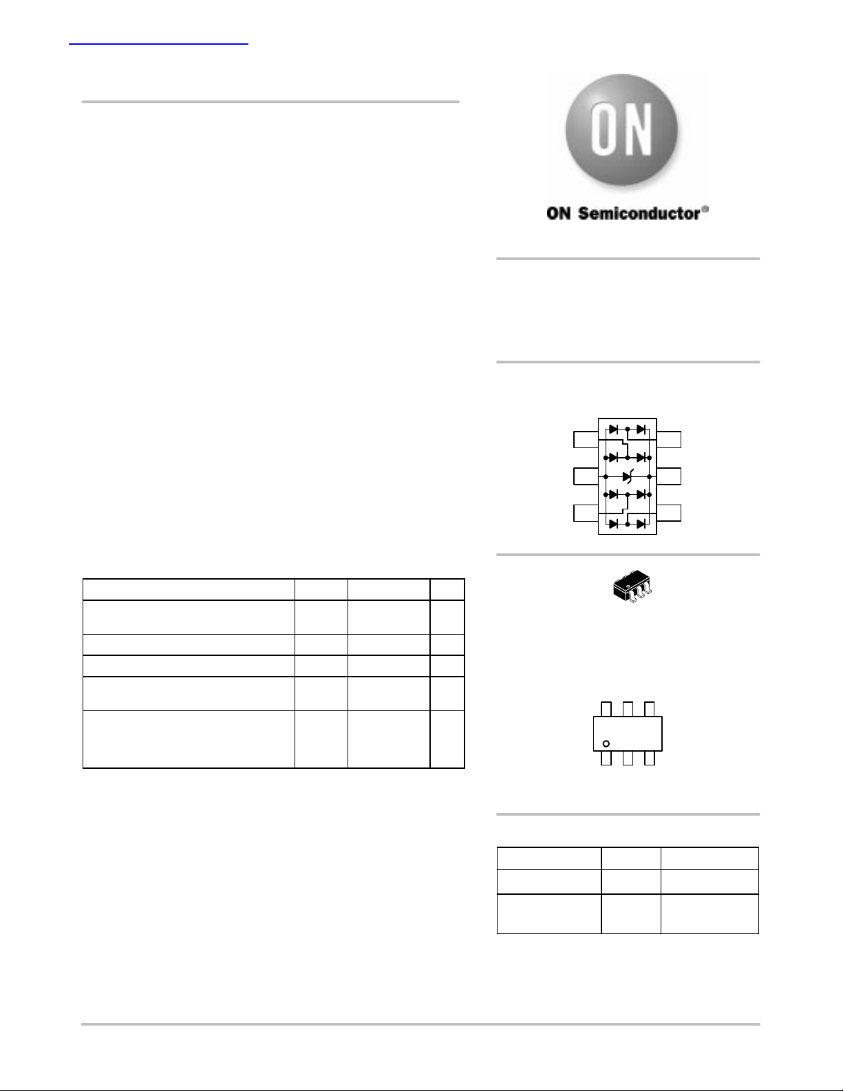
TSOP−6 LOW CAPACITANCE
DIODE TVS ARRAY
500 WATTS PEAK POWER
6 VOLTS
PIN CONFIGURATION
AND SCHEMATIC
I/O 1
V
2
N
I/O 3
6
1
TSOP−6
CASE 318G
PLASTIC
MARKING DIAGRAM
M
63
63 = Specific Device Code
M
= Date Code
ORDERING INFORMATION
Device Package Shipping
6 I/O
5 V
4 I/O
P
Semiconductor Components Industries, LLC, 2005
March, 2005 − Rev. 1
NUP4201MR6T1 TSOP−6 3000/Tape & Reel
NUP4201MR6T1G TSOP−6
(Pb−Free)
†For information on tape and reel specifications,
including part orientation and tape sizes, please
refer to our Tape and Reel Packaging Specification
Brochure, BRD8011/D.
1 Publication Order Number:
3000/Tape & Reel
NUP4201MR6/D
NUP4201MR6
ELECTRICAL CHARACTERISTICS (T
Parameter
Reverse Working Voltage V
Breakdown Voltage V
Reverse Leakage Current I
Clamping Voltage V
Clamping Voltage V
Maximum Peak Pulse Current I
Junction Capacitance C
Junction Capacitance C
Symbol Conditions Min Typ Max Unit
=25°C unless otherwise specified)
J
RWM
(Note 2) 5.0 V
IT=1 mA, (Note 3) 6.0 V
BR
V
R
C
C
PP
J
J
= 5 V 5.0 A
RWM
IPP = 5 A (Note 4) 12.5 V
IPP = 8 A (Note 4) 20 V
8x20 s Waveform 25 A
VR = 0 V, f=1 MHz between I/O Pins and GND 3.0 5.0 pF
VR = 0 V, f=1 MHz between I/O Pins 1.5 3.0 pF
2. TVS devices are normally selected according to the working peak reverse voltage (V
or continuous peak operating voltage level.
is measured at pulse test current IT.
3. V
BR
4. Non−repetitive current pulse per Figure 1 (Pin 5 to Pin 2)
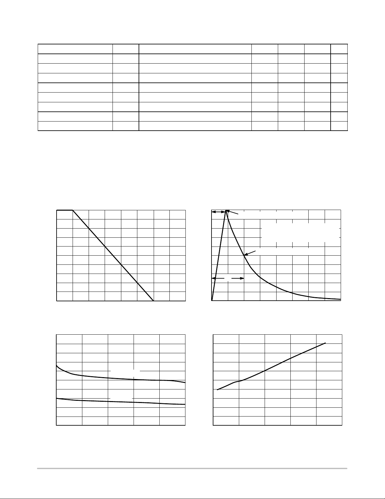
TYPICAL PERFORMANCE CURVES
(TJ = 25°C unless otherwise noted)
100
90
80
70
60
50
40
30
20
PEAK POWER DISSIPATION (%)
10
0
0 25 50 75 100 125 150 175 200
, AMBIENT TEMPERATURE (°C)
T
A
Figure 1. Pulse Derating Curve
100
t
r
90
80
70
60
50
40
30
20
% OF PEAK PULSE CURRENT
10
0
0204060
Figure 2. 8 × 20 s Pulse Waveform
), which should be equal or greater than the DC
RWM
PEAK VALUE I
RSM
@ 8 s
PULSE WIDTH (tP) IS DEFINED
AS THAT POINT WHERE THE
PEAK CURRENT DECAY = 8 s
HALF VALUE I
t
P
/2 @ 20 s
RSM
t, TIME (s)
80
5.0
4.5
4.0
3.5
3.0
I/O−Ground
2.5
2.0
1.5
I/O lines
1.0
JUNCTION CAPACITANCE (pF)
0.5
0.0
01
V
2345
, REVERSE VOLTAGE (V)
BR
Figure 3. Junction Capacitance vs Reverse V oltage
http://onsemi.com
20
18
16
14
12
10
8
6
4
CLAMPING VOLTAGE (V)
2
0
010
20 30 40 50
PEAK PULSE CURRENT (A)
Figure 4. Clamping Voltage vs. Peak Pulse Current
(8 x 20 s Waveform)
2
 Loading...